I. INTRODUCTION
In recent years, photovoltaic (PV) devices have attracted considerable attentions due to the growing energy crisis.Reference Chopra, Paulson and Dutta1–Reference Grätzel4 As for them, carrier separation is an essential procedure during the step of energy conversion, which is traditionally carried out by p–n junction.Reference Kayes, Atwater and Lewis5 And recently, heterostructures (HSs) with type-II band alignment have been proposed as an alternative candidate to implement carrier separation,Reference Zhang, Wang and Mascarenhas6 thus many kinds of type-II HSs such as ZnO/ZnS, ZnO/ZnTe, and ZnO/ZnSe have been suggested and developed.Reference Schrier, Demchenko, Wang and Alivisatos7, Reference Wang, Chen, Zhou, Zhang, Yan, Pern and Mascarenhas8 Effective bandgap of 2.37, 1.17, and 1.84 eV were theoretically predicted for the ZnO/ZnS, ZnO/ZnTe, and ZnO/ZnSe HSs, respectively, by Y. Zhang and J. Schrier group.Reference Schrier, Demchenko, Wang and Alivisatos7, Reference Wang, Chen, Zhou, Zhang, Yan, Pern and Mascarenhas8 However, these values are still different from the optimal bandgap (about 1.45 eV) based on the Shockley–Queisser detailed balance theory.Reference Shockley and Queisser9 Hence, it is quite necessary to modify the bandgap for the realization of highly efficient solar cell. Among the various HSs, the ZnO/ZnSe HS can offer larger valence band offset (VBO), which is more favorable for the high separation efficiency of the electrons and holes. Furthermore, the large lattice mismatch between the ZnO and ZnSe as well as the two types of phase structures [wurtzite (WZ) or zinc blende (ZB)] of ZnSe endows the ZnO/ZnSe HS with tunable electronic structures. In the light of these advantages, the ZnO/ZnSe HS is expected to reduce its effective bandgap to match the solar spectrum for solar cell applications by tuning the interfacial transition in spite of the large bandgap for either the ZnO or ZnSe semiconductors. Recently, well-aligned ZnO/ZnSe core/shell nanowire arrays have been fabricated, and the effective bandgap was reduced to as low as 1.60 eV by interfacial transition.Reference Wang, Chen, Zhou, Zhang, Yan, Pern and Mascarenhas8, Reference Wu, Zhang, Zheng, Lin, Chen, Huang, Wang, Huang, Li and Kang10 However, the dependences of the effective bandgap or electronic structures on the heterojunction interface, strain, misfit stress field, etc. are still unclear, and little is studied on the microscopic mechanism of the carrier separation and the optimizations of solar cell materials. Therefore, in this work, the electronic structures of ZnO (WZ)/ZnSe (WZ) and ZnO (WZ)/ZnSe (ZB) HSs were investigated by first-principle calculations to explore their applications for the solar cells. The VBO and the effective bandgap were calculated to investigate the band alignment features of the HSs. The spatial distributions of partial charge densities were plotted to directly observe the separation behavior of electrons and holes as well as the current transportation features. Finally, the optimal structure of ZnO (WZ)/ZnSe (WZ)/ZnSe (ZB) HS for the solar cell applications was proposed and discussed.
II. COMPUTATIONAL DETAILS
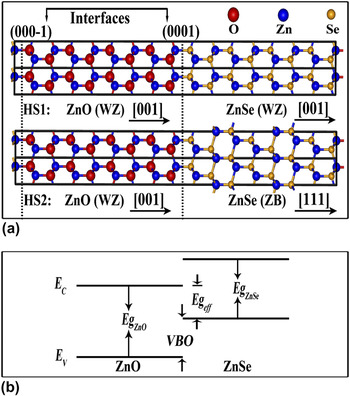
During the epitaxial growth of ZnSe on the WZ ZnO, the ZnSe may appear in two types of crystal phase, i.e., the stable ZB phase and the metastable WZ phase, resulting in two kinds of ZnO (WZ)/ZnSe (WZ) and ZnO (WZ)/ZnSe (ZB) HSs. Therefore, in this work, the unstrained ZnO (WZ)/ZnSe (WZ) and ZnO (WZ)/ZnSe (ZB) HSs (denoted as HS1 and HS2, respectively) with the width of 16 bilayers along the WZ [001] or the ZB [111] direction were constructed repeatedly in a superlattice and then relaxed, as shown in Fig. 1(a). Two types of interfaces were located at the zeroth bilayer and the eighth bilayer, denoted as (000-1) and (0001) interfaces, respectively.
(a) Structures of the ZnO (wurtzite)/ZnSe (wurtzite) [ZnO (WZ)/ZnSe (WZ)] and the ZnO (wurtzite)/ZnSe (zinc blende) [ZnO (WZ)/ZnSe (ZB)] heterostructures (HSs). (b) Band diagram of the ZnO/ZnSe HS.

The first-principle calculations were carried out by the Vienna “ab initio” simulation package.Reference Wu, Zhang, Zheng, Lin, Chen, Huang, Wang, Huang, Li and Kang10–Reference Kresse and Joubert13 The electron–ion interactions were described by the projector augmented wave method with generalized gradient approximation correction.Reference Blöchl14, Reference Perdew and Wang15 The electronic wave functions were expanded by using a plane-wave basis set with 500 eV cutoff. The Brillouin zone integrations were performed for (9 × 9 × 3) Monkhorst-Pack grids.Reference Monkhorst and Pack16 The Zn-3d electrons were used as the valence electrons. The geometry optimizations were preformed by relaxing all degrees of freedom using the conjugate gradient algorithm, in which the convergences were set to 1 × 10⁻³ and 1 × 10⁻⁴ eV for the ions and the electrons, respectively.
To calculate the effective bandgap (Eg eff) of HSs, a simple band diagram is introduced, as shown in Fig. 1(b). The Eg eff can be given by

where Eg ZnO is the bandgap of ZnO, and VBO stands for the valence band offset. Considering the inaccurate calculated value of Eg ZnO by using DFT methods, the common experimental value of 3.25 eV is adopted in the calculation.Reference Cheng and Chien17 Additionally, the calculated VBO is relatively accurate for its independence on the conduction band levels, which can be indirectly obtained byReference Van de Walle and Martin18

where Δ is the step of the macroscopic electrostatic potential across the interface and ΔE VB is the valence-top difference of the two bulk materials. The
 is expressed as
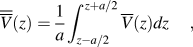
where a is the lattice constant and  stands for the microscopic average electrostatic potential.Reference Peressi, Binggeli and Baldereschi19
III. RESULTS AND DISCUSSION
The total energies were calculated to compare the stability of the above two HSs. The calculated total energies for HS2 is about 82 eV lower than that of HS1, demonstrating a more stable structure. Nevertheless, the slight difference between them implies that the HS1 structure is metastable and can be formed in special stress condition. Generally, the stress decreases dramatically with the increase of epilayer thickness, and thus metastable ZnSe (WZ) layer will transform into stable ZnSe (ZB) structure when the thickness is beyond the critical value. In experiment, both structures have been observed in the practical epitaxial growth.Reference Zheng, Wu, Yang, Li and Kang20, Reference Zhang, Cai, Li, Chen, Lai and Kang21
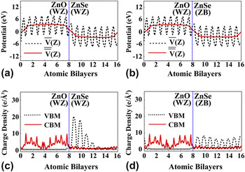
As for solar cell materials, the efficient bandgap (Eg eff) is a key parameter because it limits the absorption threshold of solar light. For the ZnO/ZnSe HS, the absorption threshold could be extended to a longer wavelength by interfacial transition and the Eg eff could be smaller than the individual materials. To get the Eg eff, the  and
 for both HSs were calculated. As shown in Figs. 2(a) and 2(b), the
 exhibits oscillation curves, whereas the
 is almost smooth, demonstrating a good filtering effect. The Δ
 of HS1 and HS2 is estimated to be −5.30 and −5.54 eV, respectively. And the ΔEVB is 7.04 and 7.10 eV, respectively. With the use of the Eqs. (2) and (1), the VBO is calculated to be 1.74 and 1.56 eV, and the Eg eff is 1.51 and 1.69 eV, respectively. It should be noted that the bandgap can be affected by material structure, strain, and polarization field.Reference Schrier, Demchenko, Wang and Alivisatos7 As a result, there is a slight difference between the calculation results and experimental values reported in Refs. Reference Wang, Chen, Zhou, Zhang, Yan, Pern and Mascarenhas8 and Reference Wu, Zhang, Zheng, Lin, Chen, Huang, Wang, Huang, Li and Kang10. In spite of these, it can be concluded that HS1 has a lower bandgap than HS2, and the absorption range for HS1 is extended to longer wave length region by the interfacial transition, which is favorable for PV applications.
The  (dash line) and
 (solid line) for (a) HS1 and (b) HS2. The partial charge densities of valence band maximum (VBM) (dash line) and conduction band minimum (CBM) (solid line) for (c) HS1 and (d) HS2.

To visualize the distributions of the associated square wavefunction, the partial charge density profiles were used. The partial charge densities in both the conduction band minimum (CBM) and the valence band maximum (VBM) were calculated and plotted along c-axis to observe the spatial separation behaviors of the electrons and holes. As shown in Figs. 2(c) and 2(d), the CBM and VBM states are distributed in the ZnO and ZnSe layers, respectively. The densities in CBM are almost the same for both HSs. It is noteworthy that most of the densities in VBM for HS1 accumulate around the interfacial layers of the ZnSe region, and the maximal densities in VBM are almost twice of that for HS2. Furthermore, the percentage of the holes is about 98% in the ZnSe (WZ) regions of HS1, higher than that of about 95% in the ZnSe (ZB) regions of HS2, demonstrating a slightly higher separation efficiency.
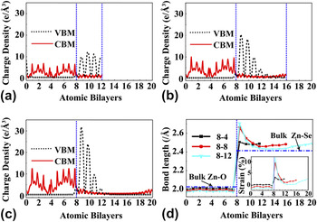
The difference of the densities in VBM may be caused by the different internal field, including the polarization field f pol and stress field f str induced by the interfacial misfit in HS1 and HS2. To clarify the physical origins of the difference in the distribution of holes, HSs with different epilayer widths were constructed to modify the interfacial misfit strains and their partial charge densities were calculated with the results in Figs. 3(a)–3(c). For the HS with four ZnSe bilayers, the distribution of holes is more uniform in the whole ZnSe layers, whereas the other two HSs exhibit a dramatic decrease away from the interface. Since the polarization field f pol exists in the three HSs, the distribution difference demonstrates a weak influence from f pol. The stress field f str can be observed by the bond length variation of Zn–O or Zn–Se along the c-axis in different HSs. As shown in Fig. 3(d), the ZnSe layers are subject to distinct tensile strain along the c-axis while the ZnO layers are under small compressive strain. For the HSs with thicker ZnSe, the strains are even larger (up to 12%) at the interfaces, as shown in the inset of Fig. 3(d). The strain will bring about energy band bending, resulting in the accumulation of holes at the interfaces, which is consistent with the distribution of holes in Figs. 3(a)–3(c). From this viewpoint, the stress field f str, rather than the polarization field f pol, is mainly responsible for the high separation efficiency of the holes.
The partial charge densities of VBM (dash line) and CBM (solid line) in HS1 with fixed ZnO (WZ) width of 8 bilayers and varied ZnSe (WZ) width of (a) 4 bilayers, (b) 8 bilayers, and (c) 12 bilayers along the c-axis. (d) The relevant bond lengths of Zn–O and Zn–Se for HS1 with different ZnSe (WZ) bilayers. The inset is the relevant strains.

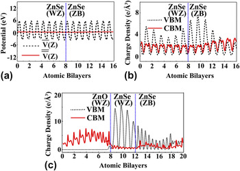
Although the holes can be effectively separated near the interfaces with a large strain, the hole densities decrease to nearly zero as the strain decreases away from the interface. This behavior will restrict the hole transportation. In practical applications, a comprehensive consideration should be given to balancing the carrier separation and current transportation efficiencies. By comparing Fig. 3(a) with Fig. 2(d), the HS1 with four ZnSe bilayers is under a moderate strain and the carrier separation efficiency is higher than that of HS2. In addition, the hole distribution in ZnSe layers are more uniform than that of thicker ZnSe (WZ) layers, as shown in Figs. 3(a)–3(c). On the basis of these, the HS1 with thin ZnSe layers is a favorable structure to meet the demands of both the carrier separation and the current transportation efficiencies. Practically, the metastable WZ ZnSe will transform into the stable ZB phase when the layer is beyond the critical thickness during the epitaxial growth, resulting in a ZnSe (WZ)/ZnSe (ZB) structure. To understand its electronic structures, the  ,
 , and the partial charge densities were calculated. As shown in Fig. 4(a), the
 exhibits a flat line along the c-axis, demonstrating a tiny VBO. Furthermore, the separation of the electrons and holes is invisible according to the partial charge densities in Fig. 4(b). Hence, the ZnSe (ZB) can be used as a current transportation layer for the ZnO (WZ)/ZnSe (WZ) HS.
(a) The  (dash line) and
 (solid line) for the ZnSe (WZ)/ZnSe (ZB) HS. (b) The partial charge densities VBM (dash line) and CBM (solid line) for the ZnSe (WZ)/ZnSe (ZB) HS. (c) The partial charge densities of VBM (dash line) and CBM (solid line) for the ZnO (WZ)/ZnSe (WZ)/ZnSe (ZB) HS.

Based on the above analysis, the optimal structure for the PV applications is proposed to be the ZnO (WZ)/ZnSe (WZ)/ZnSe (ZB) HS. The partial charge densities of the CBM and VBM for this HS were calculated with the results in Fig. 4(c). As expected, the separation of electrons and holes occurs in the interface between the ZnO and the ZnSe, and the holes distribute in the whole ZnSe layer with a ratio of about 6:4 for the ZnSe (WZ) and ZnSe (ZB) regions, demonstrating a good transportation for the holes. Favorably, the hole separation efficiency is higher than that of HS without ZB ZnSe [as shown in Fig. 3(a)]. In addition to the smaller Eg eff of 1.51 eV, the ZnO (WZ)/ZnSe (WZ)/ZnSe (ZB) HS has potential to realize a solar cell with near-infrared response.
IV. CONCLUSIONS
In summary, we investigated the electronic structures of the ZnO (WZ)/ZnSe (WZ) and the ZnO (WZ)/ZnSe (ZB) HSs by the first-principle calculations. The calculated effective bandgap of 1.51 eV for the ZnO (WZ)/ZnSe (WZ) HS is very close to the optimal bandgap of 1.45 eV in solar cell devices and is favorable for the PV applications. The partial charge densities demonstrate that the ZnO (WZ)/ZnSe (WZ) HS has a higher hole separation efficiency at the interface due to the stronger stress field. In addition, the strained ZB ZnSe layer is introduced to transport the separated holes from the WZ ZnSe layer, and an optimal structure of ZnO (WZ)/ZnSe (WZ)/ZnSe (ZB) HS is proposed to realize a solar cell with near-infrared response.
ACKNOWLEDGMENTS
The work was supported by “973” Program (2011CB925600), the National Natural Science Foundations of China (60827004, 61106008, 61106118, and 90921002), the Natural Science Foundations of Fujian Province (2010J01343 and 2011J01362), the fundamental research funds for the central universities (2011121042 and 2011121026), and the Science and Technology Programs of Fujian Province and Xiamen.