Introduction
Compact filters with high roll-off, wide stopband with transmission zeros (TZs) and low insertion loss are a massive requirement for communication system [Reference Hong1–Reference Chen, Hu, Qiu and Chu2]. An approach to achieve microwave components compactness has been suggested by revolutionary properties of metamaterial (MTM) such as composite right-/left-handed (CRLH) structure [Reference Caloz and Itoh3]. CRLH transmission line (TL) consists of a series LC circuit and shunt parallel LC circuit [Reference Choudhary and Chaudhary4]. On contrast, the dual version of CRLH unit cell (D-CRLH) has a series parallel LC tank circuit and a shunt series LC tank circuit [Reference Caloz5]. The D-CRLH TL exhibits left-handed (LH) band at higher frequency and right-handed (RH) band at lower frequency, opposite to CRLH TL which has LH band at lower frequency and RH band at higher frequency [Reference Shen, Che, Feng and Xue6].
The conventional stepped impedance approach for designing a low-pass filter (LPF) is based on cascading of low- and high-impedance TL section, but it offers narrow stopband bandwidth and requires more number of segments to achieve high roll-off [Reference Dehghani, Karimi, Lalbakhsh and Maki7]. A funnel path resonator and triangular path resonator using low and high impedance has been used in [Reference Raphika, Abdulla and Jasmine8] to achieve high roll-off. Using open-ended vialess CRLH TL structure, an LPF has been proposed with compact size and enhanced the selectivity/roll-off rate [Reference Kumar, Choudhary and Chaudhary9]. An LPF has been designed using defected ground structure (DGS) to reduce the size of filter [Reference Bhat, Jha and Singh10]. In [Reference Xiao, Sun and Li11], DGS and complementary split ring resonator with stepped impedance resonator have been used to get sharper roll-off and compactness. By using the open stub microstrip line on top of the substrate and DGS, an LPF has been proposed with wide rejection band and high selectivity [Reference Mallahzadeh and Bod12]. In [Reference Kumar and Parihar13], a hexagonal shape with stepped impedance resonator in shunt has been used to form elliptical LPF, which gives wide stopband and compactness. An LPF has been presented in [Reference Omar, Dib, Hettak, Scardelletti and Shubair14], using coplanar waveguide feed with improved rejection band. LPF with ultra-wide stopband response has been presented using stepped impedance hairpin resonator and radial stub [Reference Ma and Yeo15, Reference Hsieh and Chang16]. Compared with previous works, the proposed filter has the advantages of compact size, minimum insertion loss, high roll-off rate, and easy fabrication. As per author literature survey, the LPF using D-CRLH resonator has not been presented earlier.
In this paper, an LPF has been designed based on D-CRLH MTM resonator with wide rejection band and three TZs within the rejection band. The filter has been designed using one D-CRLH in T-Type configuration. The TZs are controlled by the D-CRLH cell elements. The LPF provides minimum insertion loss, sharp roll-off, wide stopband bandwidth, and good figure of merit (FOM) with compact size. The filter is suitable for global system for mobile (GSM: 0.8–0.96, 1.71–1.88, 1.85–1.99 GHz), long-term evolution (LTE: 1.71–1.88, 2.3–2.4, 2.5–2.69 GHz), and Wi-Fi (2.4–2.49 GHz) applications.
D-CRLH unit-cell resonator
D-CRLH unit-cell resonator: design
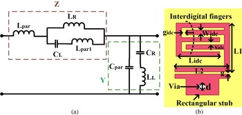
As mentioned earlier, the proposed filter resonator has been designed using one D-CRLH unit cell. The equivalent circuit of the designed D-CRLH resonator is shown in Fig. 1(a). This circuit is composed of a series parallel LC tank circuit (L R and C L) and a shunt series LC tank circuit (L L and C R). The elements L par and C par are added to the circuit to compensate for parasitic inductance and capacitance in the hosting microstrip TL. Also, the L par1 was included in the design to compensate any parasitic inductance of the used distributed capacitor (C L). Similar type of equivalent circuit has been proposed in [Reference Choudhary, Mishra, Kumar and Chaudhary17] to design a bandpass filter using interdigital capacitor (IDC) and meander line.
The unit cell of the proposed DCRLH resonator. (a) The equivalent lumped circuit model. (b) Layout. (All dimensions are in mm: L idc = 3.5, W idc = 0.4, S idc = 0.25, g idc = 0.4, g = 0.2, d = 0.7, L s = 3, W s = 1.5, L2 = 6.0.)

The objective of the proposed filter is to allow passing all low frequencies wireless services and stopping other WLAN and WiMAX frequencies (from 3.0 to 6.3 GHz). Hence, the D-CRLH resonator has been designed to achieve several design specifications. These specifications are: (i) to achieve a low-pass cut-off frequency at f c1 = 3.0 GHz; (ii) to achieve a wide rejection stopband, so that the upper frequency band for the stopband is f c2 = 6.3 GHz. Within the rejection band, two TZs were designed such that f z1 = 3.5 GHz and f z2 = 5.7 GHz. These two zeros frequencies were designed to define a roll-off sharping factor (10%; the TZ frequency difference from cut-off frequency divided by their center frequency). In other quantitative words, for first zero, the Δf zc = 0.5 GHz and f ozc = 3.25 GHz, and for the second zero, Δf zc = 0.6 GHz and f ozc = 6.0 GHz.
 $$ROSF = \displaystyle{{\Delta f_{zc}} \over {\,f_{ozc}}}.$$
As an initial design for the resonator cut-off frequencies, the dispersion propagation of periodic network analysis was employed as in (2) [Reference Daw, Abdalla and Hennawy18, Reference Abdalla and Fouad19]
 $$\cos (\beta d) = 1 + \displaystyle{1 \over 2}Z\,Y,$$
where,
 $$\eqalign{&Z = Z_1 + \displaystyle{{Z_2Z_3} \over {Z_2 + Z_3}},\quad Z_1 = j\omega L_{\,par},\quad \cr &Z_2 = j\omega L_{\,par1} + \displaystyle{1 \over {\,j\omega C_L}},\quad {\rm and}\quad Z_3 = j\omega L_R$$
 $$\eqalign{&Y\, = Y_1 + Y_2,\quad Y_1 = j\omega C_{Par},\quad {\rm and}\quad \cr &Y_2 = 1/\left( {\,j\omega L_L + \displaystyle{1 \over {\,j\omega C_R}}} \right).}$$
The cut-off frequencies (f c1 and f c2) in this case are obtained by satisfying the condition βd = π in (2). The value of C par is far less than the other capacitance values and can be ignored. Thus, the cut-off frequencies can be extracted mathematically as:
 $$\left. {-4 = \displaystyle{{\,j\omega L_R\lpar {1-\omega^2L_{\,par}C_L} \rpar } \over {\lpar {1-\omega^2{\rm (}L_{\,par} + L_R{\rm )}C_L} \rpar }}\displaystyle{{\,j\omega C_R} \over {1-\omega^2L_LC_R}}\pi} \right \vert\!\!\!\quad f = 3\,{\rm GHz},6.3\,{\rm GHz}{\rm.} $$
On the other side, the TZs were designed by adjusting zero transmission coefficient as
 $$S_{21} = \displaystyle{2 \over {A + D + B/Z_0 + CZ_0}}\vert {_{\,f = 3.5\,{\rm GHz},5.7\,{\rm GHz}}} = 0,$$
where,
 $$\eqalign{A &= 1 + ZY \cr&= \displaystyle{\matrix{1-\omega ^2{\rm [(}L_L + L_{\,par} + L_R{\rm )}C_R + {\rm (}L_{\,par1} + L_R{\rm )}C_R{\rm ]} \cr + \omega ^4{\rm [}C_LL_R{\rm (}1 + L_{\,par}C_R{\rm )} + L_{\,par}C_L{\rm (}1 + L_{\,par}C_R + C_R{\rm )]}} \over 1-\omega ^2{\rm [}C_LL_R + L_LC_R{\rm ]} + \omega^4 C_L L_R L_L C_R}},$$
 $$B = Z = j\omega L_{\,par} + \displaystyle{{\,j\omega L_R\lpar {1-\omega^2L_{\,par1}C_L} \rpar } \over {1-\omega ^2{\rm (}L_{\,par1} + L_R{\rm )}C_L}},$$
 $$C = Y\approx \displaystyle{{\,j\omega C_R} \over {1-\omega ^2L_LC_R}},$$
 $$D = 1.$$
It is worth to comment that TZs can also be obtained analytically from impedance and admittance values by imposing Z = ∞ (in 2b) in the series LC branch and Y = ∞ in (2c) in the parallel LC resonator [Reference Li and Wu20]. Hence, having Z = ∞, the TZ frequency (f z1) is
 $$f_{z1} = \displaystyle{1 \over {2\pi \sqrt {C_L{\rm (}L_{\,par1} + L_R{\rm )}}}}. $$
Also, by substituting Y = ∞, the TZ frequency becomes
 $$f_{z2} = \displaystyle{1 \over {2\pi \sqrt {L_LC_R}}}. $$
Based on the previous design equation procedures (3)–(6), and ignoring the parasitic elements values, the lumped element values (L R = 1.35 nH, C L = 0.35 pF, C R = 0.57 pF, and L L = 3.9 nH) were calculated.
In other words, the design was based on four equations. The first two were for adjusting the cut-off frequencies (using (3) twice as f c1 = 3.0 GHz and f c2 = 6.3 GHz), and the other two equations were for adjusting the TZs (using (6) twice as f z1 = 3.5 GHz and f z2 = 5.7 GHz). Since parasitic elements were ignored in calculation, to find the values of L R, C L, C R and L L. Next, they were fine tuning in the circuit model simulation/EM simulation.
It is worth to comment that although the D-CRLH configuration in Fig. 1 is not directly relevant to that of LPF, but at low frequencies, the values of C L and L L impedances become insignificant. Hence, by removing them of the equivalent circuit in Fig. 1, it becomes a typical low pass. However, at higher frequencies, the circuit is a bandstop filter that enables the design of wide stopband with TZs.
D-CRLH unit-cell resonator: synthesis
The validation for the resonator circuit performance is made clear by emphasizing the simulated scattering parameter magnitudes as shown in Fig. 2, where it can be seen the almost resonator cut-off frequencies and TZs. The realization of this circuit has a layout shown in Fig. 1(b). The parallel LC tank is realized as an IDC with one connected finger to represent the parallel inductance. The series LC tank uses a gap capacitance (a gap (g) between two parallel metallic patches) in shunt with short circuited stub connected to ground by via. The resonator is printed on a low-cost FR4 epoxy glass substrate with dielectric constant 4.4, loss tangent 0.02, and height of substrate 1.6 mm. Based on lumped element values of equivalent circuit model, synthesize of the loading elements has been calculated using deign formulas for distributed elements as [Reference Bahl21].
 $$C_L{\rm (}pF{\rm )} = {\rm (}\varepsilon + 1{\rm )}Lidc{\rm [(}N_f-3{\rm )}A_0 + A_1{\rm ],}$$
 $$\eqalign{L_R{\rm (}nH{\rm )} = 2 \times 10^{-4}L\left[ {ln \left( {\displaystyle{L \over {Widc + t}}} \right) + 1.193 + \displaystyle{{Widc + t} \over {3L}}} \right].Kg,}$$
 $$\eqalign{L_L{\rm (}pH{\rm )} &= 0.2 \left[ hsub-ln \left(\displaystyle{{hsub + \sqrt {r^2 + hsub^2}} \over r} \right) \right. \cr &\left. \quad \vphantom{\left(\displaystyle{{hsub + \sqrt {r^2 + hsub^2}} \over r} \right)}+ 1.5\left( r-\sqrt{r^2 + hsub^2} \right) \right],}$$
 $$C_R{\rm (}pF{\rm )} = 8.85 \times 10^{-3}\varepsilon _r\left( {\displaystyle{{L2 \times Widc} \over g}} \right),$$
 $$A_0 = 4.40\,{\rm tan}h{\rm [}0.55{\rm (}hsub{\rm /}Widc{\rm )}^{0.45}{\rm ]} \times 10^{-6},$$
 $$A_1 = 9.92\,{\rm tan}h{\rm [}0.52{\rm (}hsub{\rm /}Widc{\rm )}^{0.5}{\rm ]} \times 10^{-6},$$
 $$Kg = 0.57-0.145\ln {\rm (}Widc{\rm /}hsub{\rm ),}$$
where, ε r is the permittivity of substrate, L(L = L idc + g idc) is the length of microstrip line, t is the thickness of printed copper and h sub is the substrate thickness. N f represents the number of IDC finger and r is the radius of via.
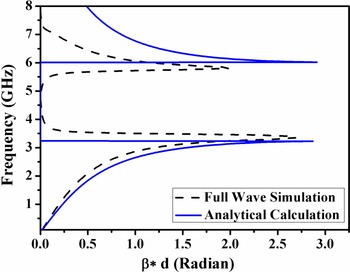
Simulated dispersion diagram of proposed D-CRLH resonator using analytical calculation (based on circuit model) and full-wave simulated scattering parameters (based on HFSS).

D-CRLH unit-cell resonator: results
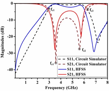
The design validation of the D-CRLH unit-cell resonator is confirmed by many methods (the dispersion diagram analysis, equivalent circuit simulation and synthesized layout full-wave simulation). During these steps, some fine adjustments to the calculated lumped values were done to achieve best results. Finally, the optimized lumped element values are L R = 1.5 nH, C L = 0.50 pF, C R = 0.65 pF, and L L = 3.1 nH. The first step in the design validation was done by plotting the dispersion diagram based on (2) for the calculated lumped elements value as shown in Fig. 2. From the figure, it depicts a RH propagation from DC up to 3.5 GHz (cut-off frequency). The wide stopband extends up to 6.3 GHz (this is equivalent to almost 100% above the RH passband). Above 6.3 GHz, the LH propagation occurs. In the second design step, the simulated scattering parameters of the resonator equivalent circuit (Fig. 1(a)) are obtained using ADS circuit simulator also shown in Fig. 2. The designed D-CRLH resonator has fulfilled the design goals (the cut-off frequencies (at 3.0 and 6.3 GHz)).
Finally, a verification of the designed dispersion diagram calculation has been done by replotting based on full-wave simulated scattering parameters for the layout in Fig. 1(a) which accounts for all parasitic elements [Reference Choudhary and Chaudhary22] as in (14). This curve is plotted in Fig. 2 using the following formula.
 $$\beta p = {\rm co}{\rm s}^{-1}\left( {\displaystyle{{1-S_{11}S_{22} + S_{12}S_{21}} \over {2S_{21}}}} \right).$$
From these two dispersion diagrams, we can claim that there are close agreements between them, which confirms all the design and synthesize calculation. Also, the full-wave simulated scattering parameters for the resonator layout are plotted in Fig. 3. The resonator synthesis verification was achieved using the full-wave simulation employing the commercial soft ANSYS Electronic Desktop (HFSS). It can be observed that the full-wave simulation of the proposed resonator realization agrees with the resonator equivalent circuit in the cut-off frequencies (at 3.0 and 6.3 GHz). Also, the full-wave simulation validates the TZs with minor shift in frequencies (f z1 = 3.48 GHz instead of 3.5 GHz in circuit simulation, f z2 = 5.75 GHz instead of 5.7 GHz in circuit simulation.
The simulated scattering parameters magnitudes of the proposed D-CRLH resonator using circuit simulator and full-wave (HFSS) simulations.

D-CRLH resonator-based filter
This section presents the design principles of proposed filter. The proposed filter structure has been designed by cascading (back-to-back) D-CRLH unit-cell resonator. Due to this configuration, extra TZs can be achieved in the filter.
D-CRLH resonator-based filter: design and structure
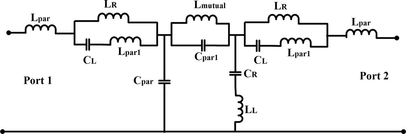
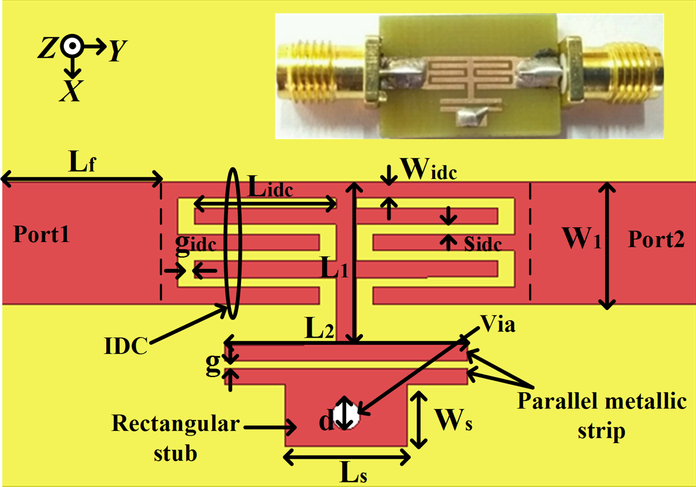
As mentioned before, the design of the proposed filter in this paper is based on symmetric configuration of the previously designed resonator. Hence, the filter equivalent circuit and its structure with fabricated prototype are shown in Figs 4 and 5, respectively. In the equivalent circuit, the filter is supposed to be a T-configuration of the same resonator.
The equivalent T circuit model of D-CRLH-based resonator low-pass filter.

The detailed geometry configuration of the D-CRLH resonator-based low-pass filter. (All dimensions are in mm: L idc = 3.5, W idc = 0.4, S idc = 0.25, g idc = 0.4, L 1 = 4, L 2 = 6, L f = 5, W 1 = 3, g = 0.2, d = 0.7, L s = 3, W s = 1.5.)

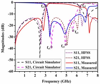
Following the designed lumped elements values in the previous section, these values were optimized based on the filter circuit model simulations so that the optimized values are L R = 1.5 nH, C L = 0.50 pF, C R = 0.65 pF, and L L = 3.1 nH. In order to tune for best filter characteristics, small values for parasitic elements and mutual inductance are added as L par = 0.5 nH, L par1 = 0.4 nH, C par = 0.43 pF, C par1 = 4.03 pF, and L mutual = 0.165 nH. Since this filter circuit configuration has three resonance circuits, then the filter can demonstrate three TZs compared with the resonator. In order to validate filter design, the designed filter (based on its circuit model in Fig. 4) has been simulated and the results are plotted in Fig. 6. It is obvious that the filter can demonstrate the third TZ at 4.95 GHz within the same bandstop bandwidth (3–6.3 GHz). To realize the filter equivalent circuit, the filter realization shown in Fig. 4 has two identical series tank circuits. However, the shunt tank circuit is common for the same two cells. It is worth to comment some changes in the filter realization dimensions for some fine tuning of filter response.
Circuit simulated, HFSS simulated, and measured scattering parameters of proposed LPF.

Parametric analysis of the designed LPF
This section introduces parametric study of proposed filter for the control of the TZs along with the cut-off frequency. This can be controlled by tuning the loading elements (C L, C R, and L L) and hence their distributed elements (spacing between interdigital fingers “S idc”, gap between parallel metallic patch “g” and the diameter of via “d”). These three parameters were selected to have different design results with the same filter size. This will give designers wide range of adjusting these frequencies based on original design presented in the previous sections.
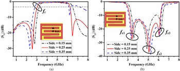
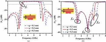
By fixing the filter parameters (as shown in Fig. 5) and changing the IDC finger spacing (S idc), the simulated results are shown in Fig. 7. In Fig. 7(a), the cut-off frequency f c of LPF shifts toward lower frequency while increasing the value of “S idc”. Figure 7(b) depicts the variation of TZ frequency with respect to “S idc” value. The first TZ f z1 decreases, f z2 increases with “S idc”, and f z3 initially decreases and remains constant after optimized value. The variation between shunt capacitance C R caused by a gap between parallel metallic patch (g) has been shown in Fig. 8. In Fig. 8(a), the cut-off frequency f c shifts toward high frequency while increasing the value of “g”. Figure 8(b) depicts that by varying the value of “g”, the second TZ remains constant and other two TZs vary.
Scattering parameters variation with respect to spacing between interdigital fingers “S idc”. (a) Cut-off frequency “f c”. (b) Transmission zero frequencies (f z1, f z2, and f z3).

Scattering parameters variation with respect to gap between parallel metallic strips “g”. (a) Cut-off frequency “f c”. (b) Transmission zero frequencies (f z1, f z2, and f z3).

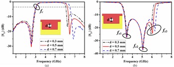
On the other hand, changing the loading via effect is illustrated in Figs 9(a) and 9(b) with respect to reflection coefficient and transmission coefficient magnitudes, respectively. In both figures, it is shown that the variation of cut-off frequency f c and TZs f zs with respect to diameter of via (d) is insignificant. However, when the value of “d” increases, f z3 increases slightly, where as other two f zs and cut-off frequency remain constant. In other words, from the figure, the small effect of the vias diameter on cut-off frequencies and TZs, except high TZ frequency, has been confirmed.
Scattering parameters variation with respect to diameter of via “d”. (a) Cut-off frequency “f c”. (b) Transmission zero frequencies (f z1, f z2, and f z3).

Filter performance analysis
Finally, the experimental performance of the proposed LPF prototype has been measured using the Network Analyzer N5221A. A comparison between the scattering parameters magnitudes for the circuit simulation, HFSS simulation, and measured date is plotted in Fig. 6. All results confirm that the filter has the same bandstop bandwidth (3.05–6.3 GHz) with three TZs at 3.35, 4.75, and 6.75 GHz. Within the filter passband (<3.05 GHz), the filter has minimum insertion loss of 0.2 dB and return loss better than 14 dB. The measured results of proposed filter are in good agreement with simulated result. However, there is a small shift in TZs due to imperfection of soldering and connector loss.
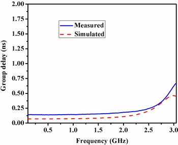
The simulated and measured group delay of proposed LPF is depicted in Fig. 10. The measured group delay is 0.13 ns in the passband. The difference between simulated and measured group delay is only 0.07 ns. The difference is mainly due to fabrication tolerance and cable loss. However, both of them have an almost typical constant slope over the bandwidth within the passband. Constant slope indicates transmission of signal with least distortion.
Simulated and measured group delay of proposed LPF.

Important parameters of LPF are roll-off rate or selectivity, relative stopband bandwidth (RSB), normalized structure size (NSS), and FOM, which are defined as in [Reference Xiao, Sun and Li11, Reference Karimi, Hamedani and Siahkamari23]
 $$\xi = \displaystyle{{\alpha _{\max} -\alpha _{\min}} \over {\,f_s-f_c}}{\rm dB}/{\rm GHz,}$$
 $$RSB = \displaystyle{{Stopband\_bandwidth} \over {Stopband\_centre\_frequency}},$$
 $$NSS = \displaystyle{{Physical\_size{\rm (}length \times width{\rm )}} \over {{\rm \lambda} _g^2}}, $$
 $$FOM = \displaystyle{{RSB \times \xi \times SF} \over {NSS \times AF}},$$
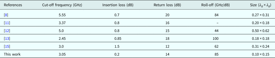
where, αmax and αmin are the 20 and 3 dB attenuation point, f s is the 20 dB stopband frequency, f c is the 3 dB cut-off frequency, and λ g is the guided wavelength at 3 dB cut-off frequency. The measured stopband bandwidth is taken for the attenuation level of −11.5 dB (from 3.2 to 6.9 GHz). AF is the architecture factor of the structure (AF = 1 for two-dimensional design and AF = 2 for three-dimensional design), SF is the suppression factor defined as stopband suppression level divided by 10. The proposed LPF offers roll-off rate 85 dB/GHz, RSB of 0.73, NSS of 0.10 λ g × 0.15 λ g, and FOM 4757. Finally, to justify the proposed structure, comparison of filter performance and size to most relevant published work is summarized in Table 1. It can be concluded that the proposed filter has advantages of low insertion loss, good roll-off rate, and compact size.
Performance comparison of proposed low-pass filter with other published filters

Conclusion
In this paper, an LPF using D-CRLH resonator with T-type circuit has been presented. The proposed resonator is composed of series parallel LC circuit and shunt series LC circuit. The experimental results of proposed filter show low insertion loss, compact size, and sharp roll-off rate with wide stopband bandwidth. The electrical size of the LPF is 0.10 λ g × 0.15 λ g, where λ g guided wavelength at cut-off frequency. The cut-off frequency and TZs are controlled with spacing between interdigital fingers.
Author ORCIDs
Mahmoud A. Abdalla http://orcid.org/0000-0001-6759-7268.
Raghvendra Kumar Chaudhary http://orcid.org/0000-0001-6186-4089
 Mr. Dilip Kumar Choudhary was born in Purnea, Bihar, India. He is pursuing Ph.D. from the Department of Electronics Engineering, Indian Institute of Technology (ISM), Dhanbad, India, and getting fellowship from MHRD, Government of India. He did his M.E. degree from Birla Institute of Technology, Ranchi, India, in 2012 and the B. Tech. degree from Biju Patnaik University, Orissa, India, in 2009. He has authored more than 22 referred journal and conference papers. He was the recipient of the International Travel Grant from DST, India, for presenting a paper in 2017 IEEE Asia Pacific Microwave Conference (APMC), Kuala Lumpur, Malaysia. He was the recipient of the Best Student Paper (Third Position) at Progress in Electromagnetics Research Symposium (PIERS), Singapore, in 2017. He is a student member of IEEE, IEEE APS, and IEEE MTT-S. His current research interests include metamaterial and its application in filter, power divider, antenna, and absorber.
 Dr. Mahmoud A. Abdalla was born in 1973. He received the B.Sc. and M.Sc. degrees in electrical engineering from the Electrical Engineering Department, Military Technical College, Cairo, Egypt, in 1995 and 2000. He received the Ph.D. degree from the School of Electrical Engineering, University of Manchester, UK, in 2009. He is now an Associate Professor and Head of Electromagnetic Waves Group in Electronic Engineering Department, Military Technical College. He was the recipient of Egyptian encouragement state prize for engineering sciences in 2014. He published more than 180 peer-reviewed journal and conference papers. His research has focused on miniaturized, multiband, and wideband microwave/millimeter antennas. Components and absorbing materials with great attention is to employ metamaterial/EBG, structures. He is a senior member of the IEEE and the European Microwave Association EuMA. He is currently a reviewer in many high ranked electromagnetic journals.
 Dr. Raghvendra Kumar Chaudhary is working as an Assistant Professor at the Department of Electronics Engineering, IIT(ISM), Dhanbad, India. He did his Ph.D. from IIT Kanpur, India, in January 2014, the M.Tech. degree from IIT(BHU), Varanasi, India, in 2009, and the B.Tech. degree from UIET Kanpur, India, in 2007. Dr. Chaudhary has authored more than 150 referred journal and conference papers. He was the recipient of the International Travel Grant from CSIR, DST, and IIT Kanpur, India. He was the recipient of the Best Student Paper Bronze Award at IEEE APACE, Malaysia, in 2010 and also recipient of the Best Paper Award at ATMS, India, in 2012. He is an Associate Editor of IEEE Access, Senior Member of IEEE, and potential reviewer of many journals and conferences such as IEEE TAP, IEEE AWPL, IET MAP, IET Electronics Letters, etc. His current research interests involve metamaterials, dielectric resonators, and computational electromagnetics.