I. INTRODUCTION
Carbon produced by removal of metal or metalloid atoms from a carbide lattice is called carbide-derived carbon (CDC).Reference Presser, Heon and Gogotsi1 The carbon layer is formed by inward conversion of the carbide into carbon, while the original shape and volume of the precursor are usually maintained (conformal transformation). CDC can be formed from silicon carbide (SiC) precursors via treatment in supercritical water,Reference Gogotsi, Nickel, Bahloul-Hourlier, Merle-Mejean, Khomenko and Skjerlie2 chlorination at high temperatures, and thermal decomposition in vacuum. The last method has been used for synthesis of aligned carbon nanotubesReference Kusunoki, Suzuki, Kaneko and Ito3 and graphene.Reference Norimatsu and Kusunoki4–Reference Cambaz, Yushin, Osswald, Mochalin and Gogotsi6 In the case of chlorination,Reference Ersoy, Mcnallan and Gogotsi7 chlorine reacts with silicon forming SiCl4gas and leaving the carbon atoms behind. On the other hand, in vacuum decomposition, Si sublimates as Si or SiO leaving carbon atoms on the surface. Depending on the process conditions, these carbon atoms self-organize forming various carbon structures on the surface.Reference Cambaz, Yushin, Osswald, Mochalin and Gogotsi6
To control the structure of the carbon formed, many research groups have been studying the formation mechanisms of carbon on SiC.Reference Norimatsu and Kusunoki4, Reference Hass, De Heer and Conrad5, Reference Ming and Zangwill8, Reference Robinson, Weng, Trumbull, Cavalero, Wetherington, Frantz, Labella, Hughes, Fanton and Snyder9 The nucleation and growth of carbon nanostructures are highly dependent on SiC surface morphology and growth conditions, such as temperature and partial pressure of oxygen.Reference Cambaz, Yushin, Osswald, Mochalin and Gogotsi6 SiC is a polar semiconductor having two nonequivalent surfaces: Si face (0001) and C face (000 $ \bar 1$). The rate of Si removal and therefore the structure of carbon formed on Si and C faces of SiC are different. Apart from surface orientation, surface defects also play an important role in determining the final carbon structure. Most of the recent studies focused on producing defect-free thin graphene films, especially monolayers or double layers.Reference Norimatsu and Kusunoki4, Reference Srivastava, He, Feenstra and Fisher10–Reference Rummeli, Rocha, Ortmann, Ibrahim, Sevincli, Borrnert, Kunstmann, Bachmatiuk, Potschke, Shiraishi, Meyyappan, Buchner, Roche and Cuniberti13 Rarely, defects, such as steps on SiC surface,Reference Sprinkle, Ruan, Hu, Hankinson, Rubio-Roy, Zhang, Wu, Berger and de Heer14 were used to control carbon formation and produce graphene ribbons. Since many results have been published on the formation of graphene monolayers on SiC, we shift the focus here to the formation of all other carbon structures on SiC. In this study, the effects of common surface defects are described and analyzed using new and published data of the authors for SiC-derived carbon films.
II. EXPERIMENTAL
A. Materials
Four different types of SiC materials were used: SiC whiskers, nanowhiskers, single crystalline wafers, and polycrystalline sintered disks. Whiskers and nanowhiskersReference Cambaz, Yushin, Gogotsi and Lutsenko15 were manufactured by a pilot plant of the Institute of General and Inorganic Chemistry, National Academy of Sciences, Ukraine, and by Dr. K.L. Vyshnyakova, Institute for Problems of Materials Science, National Academy of Sciences, Ukraine.Reference Vyshnyakova, Pereselentseva, Cambaz, Yushin and Gogotsi16 Raman spectroscopy and x-ray diffraction (XRD) studies of whiskers showed that the whiskers had beta-SiC structure. Sintered SiC disks were obtained from Saint-Gobain (Northborough, MA).Reference Erdemir, Kovalchenko, McNallan, Welz, Lee, Gogotsi and Carroll17 6H-SiC single crystal wafers, 0.37-mm thick with epi-ready polished (0001) Si face and optical quality polished (000 $ \bar 1$) C face on axis, were obtained from INTRINSIC Semiconductor Corp. (acquired by Cree Inc., Durham, NC).
B. CDC formation
CDC structures were synthesized by two different techniques: high temperature chlorination in a tube furnace and thermal decomposition in a vacuum furnace. The experimental setup used for synthesis of CDC is explained in detail in Ref. Reference Cambaz, Yushin, Gogotsi, Vyshnyakova and Pereselentseva18. Silicon extraction using chlorine was done in a conventional laboratory tube furnace with a quartz tube, which can go up to 1200 °C. Vacuum decomposition was performed using a high-vacuum furnace with graphite heating elements, which can go up to 2000 °C and down to 10−6Torr (Solar Atmosphere, Hermitage, PA).
C. Characterization techniques
A field emission scanning electron microscope (SEM), Supra 50VP (Zeiss, Jena, Germany), was used to image samples. Raman analysis was carried out using a Ramascope 1000 Raman microspectrometer (Renishaw, Gloucestershire, U.K.) equipped with a charge-coupled device detector and an optical microscope for focusing the incident laser beam to a 1–2 μm spot size. An Ar ion laser (514.5 nm) was used as an excitation source unless otherwise mentioned. A 200 kV field emission electron microscope (JEOL 2010F, Tokyo, Japan) with an imaging filter (Gatan GIF, Tokyo, Japan) was used for transmission electron microscope (TEM) studies, which were performed at the regional materials characterization facility, LRSM, at the University of Pennsylvania.
III. RESULTS AND DISCUSSION
A. Effect of grain boundaries
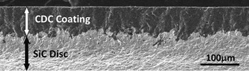
The majority of experiments on CDC synthesis by chlorination were conducted on powders and sintered ceramics.Reference Presser, Heon and Gogotsi1 Studies of CDC grown on SiC ceramics showed that the C–SiC interface was not smooth (Fig. 1), in agreement with previous studies on SiC ceramics.Reference Ersoy, Mcnallan and Gogotsi7 This is most likely because of the different reactivities of different SiC grain orientations and because the grain boundaries act as faster diffusion pathways, increasing the carbon formation rate. This rough interface provides a good adhesion of carbon to SiC, preventing spallation of the carbon film. Moreover, it was found that the carbon structures change throughout the CDC layer from C–SiC interface to surfaceReference Erdemir, Kovalchenko, McNallan, Welz, Lee, Gogotsi and Carroll17, Reference Welz, Gogotsi and McNallan19 producing carbon films with excellent tribological properties (low friction coefficient, lubrication ability in dry environments, and low wear) but reducing the ability to produce carbon with a well-defined structure. Disordered porous networks and carbon nanostructures were formed in this process.Reference Presser, Heon and Gogotsi1 To eliminate the grain boundary effects and better understand the effect of crystal orientation, single crystals were studied.
CDC layer on a sintered SiC polycrystalline ceramic sample produced by chlorination.

B. Effect of surface roughness
1. Vacuum annealing experiments
Figure 2 shows a SEM image of the optical quality polished (000 $ \bar 1$) C face of single crystalline SiC wafer after vacuum annealing at 1700 °C for 4 h. The small scratches present initially in the as-received samples have been more clearly pronounced after the carbon formation on the surface. Furthermore, when the cross section was examined, it was found that the carbon layer was not uniform. The transformation to carbon progressed deeper under the scratches. This can be explained by amorphization of SiC and the formation of vacancies and dislocations in the scratched area.Reference Gogotsi, Nickel and Kailer20 Thus, we believe that this formation of defects is responsible for both faster decomposition of SiC in the scratched areas and the greatly enhanced diffusion and evaporation of Si from the SiC surface.
SEM image of the optical quality polished (000 $ \bar 1$) C face of SiC: (a) view from top and (b) from side after vacuum annealing at 1700 °C for 4 h.

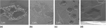
(000 $ \bar 1$) Si face studies showed that C formation starts preferentially on defects and steps on Si face. At lower temperatures (e.g., 1400 °C), voids on the carbon surface formed at defect sites are clear; however, at higher temperatures (e.g., 1800 °C), the carbon film on the surface looks more continuous and smooth (Fig. 3). Voids formed at low temperatures may be related to the agglomeration and sink of vacancies formed upon the diffusion of Si atoms through the carbon coating during the greatly accelerated SiC decomposition in the defective SiC areas. The exact mechanism of this process, however, is still not fully understood.
SEM images of SiC (0001) after vacuum annealing for 4 h at (a) 1400 °C, (b) 1500 °C, (c) 1800 °C, and (d) 1900 °C.

The pits observed at above 1800 °C were hexagonal, which is a characteristic shape for dislocations in hexagonal SiC revealed by chemical etching.Reference Zhuang and Edgar21 Hite et al.Reference Hite, Twigg, Tedesco, Friedman, Myers-Ward, Eddy and Gaskill22 suggested that screw dislocations act as preferred nucleation sites for graphene growth on C face. Interestingly, the depth and the width of the pits increased with increasing annealing temperature, supporting our hypothesis of the sink of vacancies. Indeed, higher annealing temperature shall lead to the selective evaporation of more Si near the screw dislocations. This should result in higher local content of Si vacancies, which may collapse and form a larger pit.
Surface steps also play an important role in determining the final structure of carbon on SiC. Recently, it was shown that graphene nucleates at the step edges [which can be also seen in Fig. 3(b)] and grows through the surface of the terrace.Reference Robinson, Weng, Trumbull, Cavalero, Wetherington, Frantz, Labella, Hughes, Fanton and Snyder9 Hence, decreasing surface step density and increasing the terrace area (by pretreatment like hydrogen etching) reduce the carbon nucleation rate and enable the controlled growth of single layer of graphene on terrace area. Moreover, narrow graphene ribbons can be produced on steps formed lithographically.Reference Nutt23
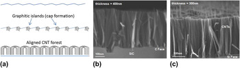
Increasing the number of surface steps, on the other hand, increases the nucleation rate, which results in carbon island formation. With the supply of external carbon to the system (e.g., by introducing CO2), we showed that these carbon islands continue to grow as carbon nanotubes (CNTs) inward SiC on both Si and C faces (Fig. 4).Reference Cambaz, Yushin, Osswald, Mochalin and Gogotsi6 Arrays shown in Figs. 4(b) and 4(c) provide the highest possible density of vertically aligned carbon nanostructures.
(a) Schematic illustration; (b, c) SEM images of CNT formation on (b) C face and (c) Si face without pretreatment (b and c are adopted from Ref. Reference Cambaz, Yushin, Osswald, Mochalin and Gogotsi6).

2. Chlorination experiments
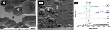
SEM images of Si and C surfaces of the 6H wafer after chlorination for 7 h at 1000 °C are shown in Figs. 5(a) and 5(b). Together with SEM studies, Raman spectra [Fig. 5(c)] taken from different regions [as numbered in Figs. 5(a) and 5(b)] of the samples showed that carbon was formed only within hexagonal pits on the Si face. On the other hand, on the C face, a continuous carbon film was formed, showing the differences in the kinetics of chlorination of Si face and C face. Besides, round-shaped hillocks were revealed on C face (e.g., spot number 3 in Fig. 5).
SEM images of (a) Si and (b) C surface of the 6H single crystalline wafer after chlorination at 1000 °C for 7 h. (c) Raman spectra taken from different regions [as numbered in panels (a) and (b)] of the sample surfaces. (1) From Si face without carbon formation, (2) from Si face inside the hexagonal etch pit, showing carbon formation, and (3, 4) from C face.

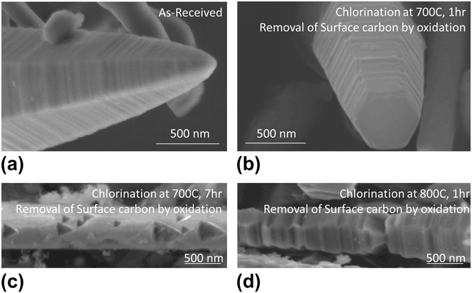
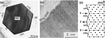
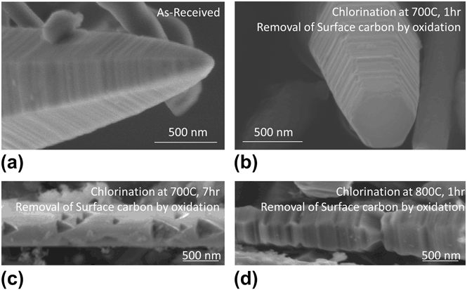
Similar experiments were performed on SiC whiskers, which also have dislocations and faceted surfaces. Formation of carbon nanostructures at the surface of whiskers through chlorination has been documented in detail in our previous paper.Reference Cambaz, Yushin, Gogotsi, Vyshnyakova and Pereselentseva18 It was shown that the transformation from SiC to carbon was conformal. The interface between SiC and carbon layer was examined after removal of carbon by oxidation in air at 500 °C for 30 min. The SEM images showed that there was no significant change in the surface morphology after chlorination at 700 °C for 1 h; however, triangular etch pits were observed on the surface of the beta-SiC whiskers after chlorination at the same temperature for a longer time (Fig. 6). Similar to wet etching of beta-SiC with KOH, these etch pits were attributed to the presence of dislocations that are associated with closely spaced parallel {111} stacking faults. This is in agreement with the Nutt’s findings,Reference Nutt23 where he investigated the cross section and the surface of the beta-SiC whisker and showed that whisker side faces {112} tend to be composed of nanofacets on alternating {111}-type planes, resulting in nanoscale roughness on the surface (Fig. 7). He additionally showed that partial dislocations exist outside the core region and extend in radial directions to the whisker sides.
SEM images of beta-SiC whiskers: (a) as-received and (b–d) after chlorination and removal of the coating by oxidation in air.
TEM images of (a) transverse and (b) longitudinal surfaces of the SiC; (c) side surface crystal model of cubic SiC whisker (T denotes twins) (modified from Ref. Reference Nutt23).

Higher reaction rate of dislocated regions can be explained by the weaker bonding in these regions, favorable energetics (release of some of the dislocation strain energy upon C formation), and faster diffusion of Cl2 and SiCl4gases through the dislocation edges. Etch pits reveal the (111) planes showing that etching is slower along <111> directions. This is most likely because each atom in {111} plane of SiC is connected to three other atoms and has only one dangling bond to react with chlorine.
Chlorination at 800 °C and removal of carbon from the surface by oxidation, however, did not show any pits. This can be explained by faster reaction kinetics at higher temperatures. At such conditions, heterogeneous SiC etching is overshadowed by the homogeneous SiC etching and more uniform carbon formation is observed over the entire surface.
C. Effect of external surface defects
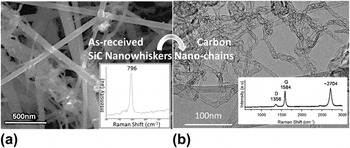
A large external surface can also be considered as a two-dimensional (2D) defect. To see the effect of the surface on thermal decomposition of SiC in samples that do not require TEM preparation, we have performed vacuum annealing on SiC nanowhiskers (nanowires). After annealing at 1700 °C for 30 min, all SiC were transformed to carbon. TEM studies showed that the produced carbon did not collapse into graphitic ribbons. Instead, tubular bamboo-like carbon structures with internal closed pores and chain-like segments formed by decomposition of β-SiC whiskers (Fig. 8). A low intensity of the disorder-induced Raman D band and a very high intensity of the 2D band at 2704 cm−1 (higher than that of the G-band) observed on these structures are only comparable to that of scrolled carbon whiskers, graphite polyhedral crystals,Reference Tan, Dimovski and Gogotsi25 and graphene.Reference Ferrari, Meyer, Scardaci, Casiraghi, Lazzeri, Mauri, Piscanec, Jiang, Novoselov, Roth and Geim26 This observation suggests that thin graphene-like walls of these cellular structures likely contain a very low concentration of defects and unsatisfied bonds.
(a) SEM image and Raman spectrum of as-received SiC nanowhiskers; (b) TEM image and Raman spectrum of nanowhiskers annealed in vacuum at 1700 °C for 30 min.Reference Cambaz24

IV. CONCLUDING REMARKS
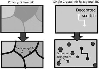
Thermal decomposition in vacuum and chlorination of SiC occur at the surface–reaction interface that advances into SiC, accompanied by removal of volatile gases (at high temperatures), such as Si, SiO, or SiCl4. The carbon formation rate is noticeably faster near various defects, such as grain boundaries, scratches, or dislocations, as schematically shown in Fig. 9. The higher concentration of vacancies in these regions allows faster diffusion, increasing the carbon formation rate. Besides, atoms at the surfaces and in other defective (higher free energy) regions of SiC are more susceptible to chemical reactions due to the weaker bonding (longer chemical bonds at the surface) or incomplete coordination of atoms. Finally, decomposition of SiC near the defects releases some of the defect-induced strain energy. The effects of the defects are particularly pronounced at conditions corresponding to relatively slow kinetics, where the rate of heterogeneous decomposition reaction is faster than the homogeneous decomposition reaction. The chlorination of SiC wafers at moderately high temperatures revealed the dislocations as hexagonal pits in hexagonal SiC. Similarly, the chlorination of cubic SiC whiskers led to selective etching of the dislocations resulting in triangular etch pits. Thus, we showed that by defect engineering, it is possible to control the structure of carbon on SiC. Selectively produced carbonaceous materials with controlled structure can find applications in electronics, sensors, and electrochemical probes. CDC films produced by chlorination or vacuum decomposition of sintered SiC find applications in dynamic seals due to their low friction coefficient.Reference Tanaka, Morita and Hibino12 One of the potential applications of dense aligned CNT arrays on SiC wafers is in heat sinks for electronics, as there exist a need to develop better thermal interface materials.
Schematic showing initial stages of carbon formation on polycrystalline ceramics and single crystal SiC.

ACKNOWLEDGMENTS
We thank Solar Atmosphere for the vacuum furnace and Intrinsic Semiconductor Corp. for SiC wafers; Centralized Research Facility of Drexel University for providing access to microscopes and spectrometers used in this study and Dr. K.L. Vyshnyakova, Institute for Problems of Materials Science, and Dr. V.G. Lutsenko, Institute of General and Inorganic Chemistry, National Academy of Sciences, Ukraine, for providing SiC whiskers. This work at Drexel University was supported by a grant from the U.S. Department of Energy, Office of Basic Energy Sciences (Grant No. DE-FG02-07ER46473).