Dramatic scaling down from flip-chip joints to microbumps
With two-dimensional large-scale integrated circuits (ICs) approaching the limit of Moore’s Law, the most promising solution is three-dimensional (3D) ICs based on chip stacking.Reference Patti1–Reference Lu3 The critical architectural element in 3D ICs is the vertical interconnect developed using through-Si via (TSV) and Cu microbump techniques. Thousands of microbumps are typically present on a given TSV chip. Pb-free solder has been employed for the microbumps to join two chips vertically. Overall, the solder joint is a very mature form of technology widely used in flip-chip technology,Reference Tu4 in which solder bumps are fabricated on Si dies, and then the Si dies are flipped over to join with polymer substrates to form vertical interconnects.
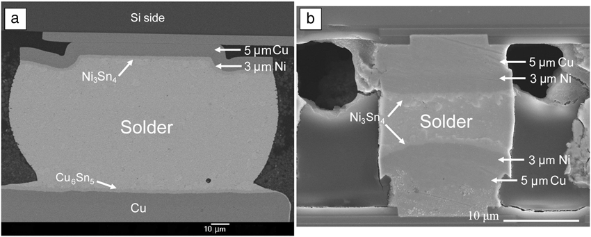
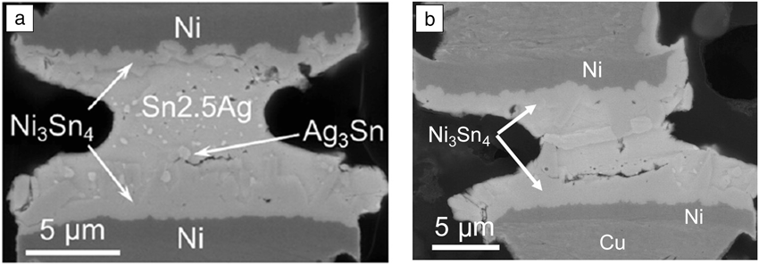
Figure 1a presents a cross-sectional scanning electron microscope image of a typical flip-chip joint with Sn2.5Ag solder.Reference Chang, Chen, Chang, Zhan, Juang and Huang5 The joint is 100 μm in diameter, and the solder is approximately 70 μm in height. As labeled in the figure, the under-bump metallization (UBM) on the chip side is 5 μm Cu/3 μm Ni. On the substrate side, the metallization is 5 μm electroless Ni on Cu traces. The solder has reacted with the metallization on the chip and substrate sides to form Ni3Sn4 intermetallic compounds of 1.0 μm thickness, such that the joint can provide electrical and thermal conduction, as well as mechanical strength to hold the chip and the substrate. The solder volume is estimated to be 6 × 105 μm3, which is much larger than that of the UBM.
Cross-sectional scanning electron microscope images showing (a) the typical structure of a flip-chip solder joint and (b) the structure of a microbump for vertical interconnects between chips.Reference Chang, Chen, Chang, Zhan, Juang and Huang5

As the microelectronic industry shifts to 3D ICs, more inputs/outputs are needed. Therefore, microbumps of 20-μm diameter are currently being adopted to be the vertical interconnects between chips. The microbumps have been successfully fabricated by reflow or thermo-compression.Reference Lin, Chiou, Yang, Chang, Lin, Liao, Hung, Lin, Tsai, Shih, Wu, Wu, Tsai, Huang, Wang, Yu, Chang, Chen, Hou, Tung, Jeng and Yu6–Reference Wright, Polastre, Gan, Buchwalter, Horton, Andry, Sprogis, Patel, Tsang, Knickerbocker, Lloyd, Sharma and Sri-Jayantha14 Typically, reflow is carried out in an oven at a temperature above the melting point of the solder for approximately one minute, whereas thermo-compression is achieved by a bonder with a compressive force above the melting point for a few seconds. Figure 1b shows the structure of a typical Sn2.5Ag microbump with 5 μm Cu/3 μm Ni UBM on both top and bottom chips. The solder height decreases to only 6.2 μm. Nevertheless, the thickness of the UBM cannot be scaled down accordingly due to consideration of metallurgical reactions. If the UBM is too thin, intermetallics (IMCs) would detach from the UBM when the UBM is consumed.Reference Liu, Kim, Tu and Totta15 Therefore, the UBM thickness of the microbump remains approximately the same as that of the flip-chip joint. It is noteworthy that the transistor has gradually scaled down in the past three decades. For example, the minimum feature length shrank from 90 nm to 65 nm nodes and from 65 nm to 45 nm nodes, which are approximately 30% reductions in dimension. However, the packaging industry experienced a dramatic scaling down from 100 μm to 20 μm, which is an 80% reduction in diameter.
Two distinct differences arise due to this shrinkage in dimension. The volume of the solder for the microbump has decreased to 1.6 × 103 μm3, which is approximately 1/400th of the volume of the conventional flip-chip joint. In addition, the solder volume is smaller than the metallization volume on both the top and bottom chips, as seen in Figure 1b. Therefore, the microbump may transform into an IMC joint after joining or after electromigration tests. Many problems may arise due to the small solder volume and the phase transformation, which are discussed later in the text. Furthermore, the cross-section for electric conduction of the microbump reduces to 1/25 of the flip-chip solder joint. The user-level current density of a microbump is around 1 × 10⁴ A/cm2, which is larger than the threshold value for electromigration of solders.Reference Yeh, Chou, Hsu, Chen and Tu16–Reference Hsu, Chou, Liu, Chen, Yao, Chou and Tu18 Thus, electromigration becomes another issue for microbumps.
Reliability issues related to a small volume of solder
The small volume of solder in a microbump may cause several reliability issues, including transformation of solder joints into IMC joints,Reference Chang, Chen, Chang, Zhan, Juang and Huang5,Reference Lin, Zhan, Juang, Lau, Chen, Lo, Kao, Tian and Tu19–Reference You, Lee, Lee and Kang23 necking or voiding induced by side wetting/diffusion on the circumference of UBM,Reference Liang, Chen and Tu24–Reference Park, Kim, Park, Kim, Son, Han, Oh, Kim and Yoo27 formation of porous Cu3Sn IMCs,Reference Panchenko, Croes, De Wolf, De Messemaeker, Beyne and Wolter28 early electromigration failures caused by specific orientations of Sn grains,Reference Lin, Chiou, Yang, Chang, Lin, Liao, Hung, Lin, Tsai, Shih, Wu, Wu, Tsai, Huang, Wang, Yu, Chang, Chen, Hou, Tung, Jeng and Yu6 and precipitation of plate-like Ag3Sn IMCs.Reference Yang, Chang, Sung and Chen29,Reference Chuang, Chen, Shih, Lai and Kao30
Transformation of solder joints into IMC joints
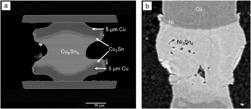
The entire microbump may transform into an IMC joint after reflow or reliability tests due to the small volume of solders.Reference Chang, Chen, Chang, Zhan, Juang and Huang5,Reference Lin, Zhan, Juang, Lau, Chen, Lo, Kao, Tian and Tu19–Reference You, Lee, Lee and Kang23 Nickel and copper are two popular UBM materials for microbumps. Three possible microbump structures are Ni/solder/Ni,Reference Lin, Chiou, Yang, Chang, Lin, Liao, Hung, Lin, Tsai, Shih, Wu, Wu, Tsai, Huang, Wang, Yu, Chang, Chen, Hou, Tung, Jeng and Yu6,Reference Hsu, Chou, Liu, Chen, Yao, Chou and Tu18 Ni/solder/Cu,Reference Huang, Zhan, Lin, Juang, Huang, Chen, Fan, Cheng, Chao, Lin, Lin and Chen31 and Cu/solder/Cu.Reference Labie, Limaye, Lee, Berry, Beyne and De Wolf22,Reference Park, Kim, Park, Kim, Son, Han, Oh, Kim and Yoo27 Cu6Sn5 IMCs have a much higher reaction rate, about five times that of Ni3Sn4 IMCs.Reference Kim and Tu32,Reference Kim, Jang, Lee and Tu33 Thus, Cu/solder/Cu microbumps can be easily transformed into IMC microbumps consisting of Cu/Cu3Sn/Cu6Sn5/Cu3Sn/Cu,Reference You, Lee, Lee and Kang23 as shown in Figure 2a. Some Kirkendall voids due to unbalanced atomic flux are formed in Cu3Sn layers and may weaken the mechanical properties of the microbump. Further heat treatment will transform the microbump into Cu/Cu3Sn/Cu.Reference Chiu, Liu, Haung and Chen34 Even though Ni has a lower reaction rate than Sn, the solder in Ni/solder/Ni can also be completely consumed and form a Ni/Ni3Sn4/Ni IMC joint after electromigration,Reference Chang, Chen, Chang, Zhan, Juang and Huang5,Reference Wei, Yu, Tung, Huang, Hsieh, Chiu, Hsiao, Chang, Lin, Liang, Chen, Yeh, Lin and Yu7 as shown in Figure 2b. Current stressing (i.e., applying high current densities) enhances the dissolution of Ni and accelerates the formation of the Ni3Sn4 IMC. For Ni/solder/Cu microbumps, ternary IMCs of (Cu,Ni)6Sn5 are formed at a rate between that of Ni3Sn4 and Cu6Sn5 IMCs.Reference Huang, Zhan, Lin, Juang, Huang, Chen, Fan, Cheng, Chao, Lin, Lin and Chen31
Cross-sectional scanning electron microscope images depicting intermetallic (IMC) microbumps. (a) IMC microbumps of Cu/Cu3Sn/Cu6Sn5/Cu3Sn/Cu formed after reflow at 260°C for 40 min, and (b) a Ni3Sn4 IMC microbump formed after current stressing by 9.6 × 10⁴ A/cm2 at 164°C for 130 h.Reference Wei, Yu, Tung, Huang, Hsieh, Chiu, Hsiao, Chang, Lin, Liang, Chen, Yeh, Lin and Yu7
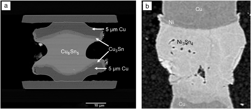
Table I lists the resistivity, elastic modulus, and melting point for Ni3Sn4, Cu6Sn5, Cu3Sn, and SnAg solders. Among the three IMCs, Ni3Sn4 is the most resistive compound. Nevertheless, when the solders react with Ni to form Ni3Sn4, the resistance of a microbump increases approximately 68%.Reference Chang, Chen, Chang, Zhan, Juang and Huang5,Reference Chang, Peng, Yang, Chen, Chang, Zhan, Juang and Huang35 However, formation of IMCs would neither cause excessive Joule heating nor accelerated electromigration damage. Instead, the three IMCs possess higher electromigration resistance than SnAg soldersReference Wei, Chen, Liu and Chen36,Reference Chen, Shih, Wei, Tung, Hsiao, Yu, Liang and Chen37 because they have higher melting points and elastic moduli than SnAg solders, as shown in Table I. With proper design of the thickness ratio of UBM materials to solders, the solders in microbumps can completely transform into IMCs, thus enhancing the electromigration resistance.Reference Chen, Shih, Wei, Tung, Hsiao, Yu, Liang and Chen37 In fact, it has been reported that the electromigration lifetime of microbumps surpasses that of flip-chip solder joints.Reference Lin, Chiou, Yang, Chang, Lin, Liao, Hung, Lin, Tsai, Shih, Wu, Wu, Tsai, Huang, Wang, Yu, Chang, Chen, Hou, Tung, Jeng and Yu6,Reference Syed, Dhandapani, Moody, Nicholls and Kelly38,Reference Wang, Lin, Chen, Chiu, Chen, Yeh, Lin, Hou, Lin, Chen, Jeng and Yu39 This is because IMC joints form during electromigration, and there is almost no current crowding effect in solders.Reference Wei, Yu, Tung, Huang, Hsieh, Chiu, Hsiao, Chang, Lin, Liang, Chen, Yeh, Lin and Yu7,Reference Chang, Peng, Yang, Chen, Chang, Zhan, Juang and Huang35,Reference Wang, Lin, Chen, Chiu, Chen, Yeh, Lin, Hou, Lin, Chen, Jeng and Yu39 The current distributes uniformly in the solder.
Resistivity, elastic modulus, and melting points for Ni3Sn4, Cu6Sn5, Cu3Sn, and SnAg solders.
On the other hand, IMCs are brittle in nature. Hence, the mechanical properties of IMC microbumps may be worse than those of microbumps of the remaining solders. Whether the three IMCs are brittle remains controversial,Reference Lee, Wang and Kim40 because both Ni-Sn and Cu-Sn microbumps can pass the temperature cycling test (TCT), in which the microbumps experience temperature cycling between –55°C and ∼125°C for 1000 cycles. Usually, when the resistance of the microbumps does not increase over 20% of their initial value after the test, the microbumps pass the test. The drop test can determine whether IMC microbumps are brittle. During drop tests, microbumps are dropped from a certain height and experience a much higher strain rate than during TCTs. However, no such results have been reported. In addition, the creep behavior of IMCs is not clear and merits more investigation.
Necking or voiding induced by side wetting/diffusion
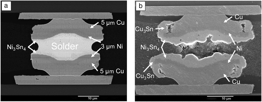
Necking or voiding induced by side wetting/diffusion becomes a serious reliability issue in microbumps, and no solution has been reported so far. Liang et al. claimed that the solder may wet the circumference of the Ni/Cu UBM during reflow.Reference Liang, Chen and Tu24 Sn atoms tend to diffuse on the circumference of Ni and Cu UBM to form Ni3Sn4 and Cu3Sn, respectively, to reduce the free energy of the system. Owing to the small solder volume, necking or voiding may occur when Sn is drawn away. Figure 3a presents an as-fabricated Cu/Ni/solder/Ni/Cu microbump with a solder height of 8 μm. After reflow at 260°C for 20 min, Sn diffused to the circumference of Ni and Cu UBM to form Ni3Sn4 and Cu3Sn, respectively.Reference Liang, Chen and Tu24 As a result, the solders between the top and bottom UBM were depleted, and necking or voiding occurred in the joint. Necking or voiding weakens both mechanical and electrical properties of the microbump. In some cases, the solders were completely depleted, as shown in Figure 3b. This phenomenon not only happens during molten-state reflow, but also takes place in solid-state aging,Reference Cheng, Chung, Pai and Chen25 thermal cycling,Reference Chan, Liao, Lin, Chuang, Huang, Yeh, Tseng and Lai26 and electromigration tests.Reference Lin, Zhan, Juang, Lau, Chen, Lo, Kao, Tian and Tu19,Reference Park, Kim, Park, Kim, Son, Han, Oh, Kim and Yoo27 Therefore, it is an urgent problem, which needs to be solved.
(a) As-fabricated Cu/Ni/solder/Ni/Cu microbump. (b) After reflow at 260°C for 20 min, side wetting occurred, and Sn diffused to the circumference of Ni and Cu under-bump metallization to form Ni3Sn4 and Cu3Sn, respectively, resulting in the complete depletion of the solder.Reference Huang, Zhan, Juang, Lin, Huang, Chenl, Fan, Cheng, Chao, Hsieh, Chen and Lau55
Formation of porous Cu3Sn IMCs
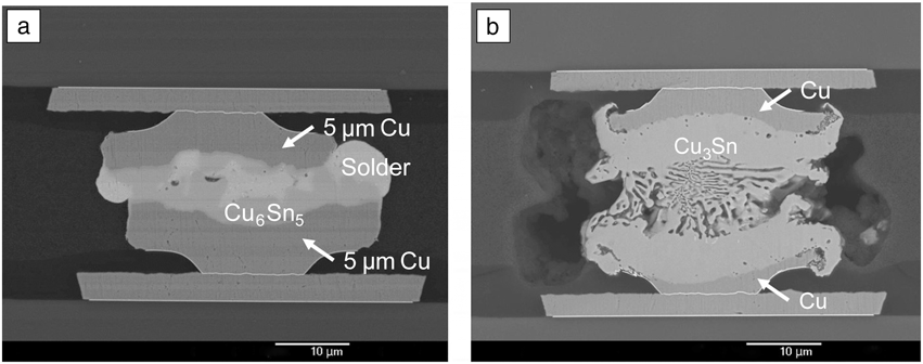
For the Cu-Sn metallurgical reaction, layer-type Cu3Sn is regarded as the terminal phase when there is a limited amount of Sn.Reference Tu4 However, Panchenko et al. reported that porous Cu3Sn started to form in Cu/solder/Cu after reflow at 260°C for two min. Side wetting was also observed in the circumference of Cu UBM.Reference Panchenko, Croes, De Wolf, De Messemaeker, Beyne and Wolter28Figure 4a shows an as-fabricated Cu/SnAg/Cu microbump with 8-μm-thick SnAg solder. After reflow for 12 h, porous Cu3Sn formed in the microbump (Figure 4b). A mechanism has been proposed to explain the formation of the porous Cu3Sn layer, as described later in the text. IMCs of Cu6Sn5 on Cu tend to transform into Cu3Sn upon continuous annealing. The process involved is either
(a) As-fabricated Cu/solder/Cu microbump with 8-μm-thick SnAg solder. (b) Porous Cu3Sn is formed in the microbump attributed to side wetting on the circumference of Cu under-bump metallization after reflow at 260°C for 12 h.Reference Panchenko, Croes, De Wolf, De Messemaeker, Beyne and Wolter28
 $${\rm{Cu}}_{\rm{6}} {\rm{Sn}}_{\rm{5}} \to {\rm{2Cu}}_{\rm{3}} {\rm{Sn + 3Sn}}$$
or
 $${\rm{Cu}}_{\rm{6}} {\rm{Sn}}_{\rm{5}} {\rm{ + 9Cu}} \to {\rm{5Cu}}_{\rm{3}} {\rm{Sn}}{\rm{.}}$$
During continuous high-temperature processing, the initially formed Cu6Sn5 joints transformed into Cu3Sn. According to Equation 1, Sn is released. The released Sn in liquid state diffuses rapidly, leading to wetting of the side of Ni and Cu UBM to form IMCs. The microbump region is thus occupied by porous Cu3Sn, indicating that porous Cu3Sn is the terminal phase for microbumps when Sn atoms diffuse to the circumference of the Cu UBM during phase transformation of Cu6Sn5 to Cu3Sn. Nevertheless, if there is enough Cu supply, the released Sn will react with Cu to form Cu3Sn, as illustrated by Equation 2. Layer-type Cu3Sn is formed in microbumps when there is no side wetting/diffusion.Reference Chiu, Liu, Haung and Chen34 The formation of porous Cu3Sn also undermines the mechanical and electrical properties. Such porous structures have not been found in Ni3Sn4 and (Cu,Ni)6Sn5.
Early electromigration failures caused by specific orientations of Sn grains
Extremely fast Cu and Ni dissolution may occur along specific Sn grain orientations.Reference Yeh and Huntington41,Reference Dyson, Anthony and Turnbull42 Lu et al. found that rapid depletion of IMCs and Ni UBM occurs along the c-axis of Sn crystals, resulting in significant damage to the joints.Reference Lu, Shih, Lauro, Goldsmith and Henderson43 The dissolution of Cu and Ni is rapid because Cu interstitial diffusivity along the c-axis is 500 times faster than that along the a- or b-axis of Sn crystals at 25°C, and the diffusivity of Ni along the c-axis is ∼7 × 10⁴ times faster than that at right angles (a- or b-axis) at 120°C.Reference Yeh and Huntington41 Therefore, Sn grain orientation plays an important role in the electromigration failure modes and lifetime of SnAg solders. The effect of Sn grain orientation on reliability issues will become more significant because some of the microbumps consist of a single Sn grain.Reference Tu, Hsiao and Chen44,Reference Tian, Chen, Kunz, Tamura, Zhan, Chang and Tu45
It has been reported that flip-chip joints with c-axis Sn grains parallel to the electron flow had shorter electromigration lifetimes than joints with Sn grains perpendicular to the electron flow.Reference Wang, Lu, Gupta, Stiborek, Shirley, Chae, Im and Ho46 This is because c-axis Sn grains parallel to the electron flow allow rapid dissolution of the Ni UBM, leading to deterioration of contact opening and shorter electromigration lifetime. The Ni UBM connects to the circuits in the chip through the contact opening, and voids may form after the Ni UBM is dissolved into the Sn grains. However, for microbumps, the effect of Sn grain orientation on electromigration lifetime is the reverse. Rapid dissolution of Ni UBM occurring in microbumps with c-axis Sn grains parallel to the electron flow transform them into IMC microbumps, resulting in a longer electromigration lifetime.Reference Lin, Chiou, Yang, Chang, Lin, Liao, Hung, Lin, Tsai, Shih, Wu, Wu, Tsai, Huang, Wang, Yu, Chang, Chen, Hou, Tung, Jeng and Yu6,Reference Chen, Shih, Wei, Tung, Hsiao, Yu, Liang and Chen37
Figure 5a–f shows the effect of Sn grain orientation on the formation of Ni3Sn4 IMCs.Reference Wei, Yu, Tung, Huang, Hsieh, Chiu, Hsiao, Chang, Lin, Liang, Chen, Yeh, Lin and Yu7c-axis Sn grains nearly perpendicular to the electron flow (high-angle grains) had a much lower IMC formation rate. The three Sn grain orientations in Figure 5b are 84.9°, 81.1°, and 85.2°. Thus, most of the solders were un-reacted, yet in the microbump in Figure 5c–d, the IMC formation rate in the center grain appeared much faster than the two grains on the periphery of the microbumps. The Ni3Sn4 IMC bridged the joint. However, some Sn grains at low angles to the electron flow were transformed into IMC grains, which have higher electromigration resistance than solder. The Sn grain in Figure 5c is at 89.9° to the electron flow, and most of the solder remained intact. Voids may form in this microbump after longer current stressing up to thousands of hours. The microbump in Figure 5c has a bridged Ni3Sn4 IMC, which will have a longer electromigration lifetime than the microbump in Figure 5e.
Cross-sectional images of microbumps after current stressing by 9.6 × 10⁴ A/cm2 at 164°C for 1–30 h. (a), (c), and (e) are scanning electron microscope images; (b), (d), and (f) are grain orientations mapped by electron backscatter diffraction (EBSD).Reference Lin, Chiou, Yang, Chang, Lin, Liao, Hung, Lin, Tsai, Shih, Wu, Wu, Tsai, Huang, Wang, Yu, Chang, Chen, Hou, Tung, Jeng and Yu6 The EBSD maps show the orientation of the remaining Sn grains after current stressing. The angle labeled in the maps represents the angle between the current direction and the c-axis of the Sn grain. Note: IMC, intermetallic.
Precipitation of plate-like Ag3Sn IMCs
SnAg alloys have been adopted as solder materials in flip-chip solder joints due to their excellent mechanical properties and precise control of the composition during electroplating. Dispersed Ag3Sn IMCs formed in the as-fabricated microbumps, as shown in Figure 6a.Reference Yang, Chang, Sung and Chen29 However, large plate-like Ag3Sn IMCs form inside the solder joints when the concentration of Ag is higher than 3.5 wt%,Reference Jang, Frear, Lee and Tu47 and cracks may initiate at the interface of these plate-like Ag3Sn IMCs and the solder when the solder joints are subjected to stress.Reference Zeng and Tu48 Therefore, the packaging industry has adopted SnAg alloys with a low Ag concentration (∼2.5 wt%) to avoid the formation of these plate-like Ag3Sn IMCs. However, plate-like Ag3Sn IMCs may still form even when low-Ag concentration solder is used. This is because during Cu-Sn or Ni-Sn interfacial reactions, the Ag atoms do not participate in the reactions, and they do not form Cu-Sn-Ag or Ni-Sn-Ag ternary IMCs. They are expelled to the molten solder during the interfacial reaction. In microbumps with small amounts of solder, when Sn is consumed by interfacial reactions, the concentration of Ag in the remaining solder continues to increase. At some point, the Ag concentration will exceed 3.5 wt%.Reference Chuang, Chen, Shih, Lai and Kao30,Reference Huang, Zhan, Lin, Juang, Huang, Chen, Fan, Cheng, Chao, Lin, Lin and Chen31 When the microbumps are cooled, plate-like Ag3Sn IMCs will then form in the microbumps. Figure 6b shows 4.0-μm-thick Sn2.5Ag microbumps after reflowing for 10 min at 260°C, respectively. As can be seen, plate-like Ag3Sn IMCs formed in the solder and Ni3Sn4 IMCs. These precipitates will adversely affect the mechanical properties of the microbumps. Therefore, the concentration of Ag in SnAg solders should be decreased with downward scaling of microbumps.
Cross-sectional backscatter scanning electron microscope images of 4.0-μm-thick Sn2.5Ag microbumps after reflowing for (a) 0 min and (b) 10 min at 260°C.Reference Yang, Chang, Sung and Chen29
Vertical interconnects by Cu-to-Cu direct bonding
Another approach to fabricating vertical interconnects is Cu-to-Cu direct bonding.Reference Chen, Lee, Andry, Tsang, Topol, Lin, Lu, Young, Ieong and Haensch49 Under ultrahigh-vacuum conditions, direct Cu-to-Cu bonding can be achieved at room temperature; however, the Cu surface needs to be cleaned prior to bonding by using a surface-activated approach, and the process is rather time-consuming.Reference Kim, Howlader, Itoh and Suga50 Under ordinary-vacuum conditions on the order of 10–3 to 10–4 Torr (0.13 to 0.013 Pa), direct Cu-to-Cu bonding can be obtained by thermal compression at temperatures exceeding 300°C for more than 30 min under compression of approximately 100 psi.Reference Tan, Peng, Fan, Li and Gao51 Nevertheless, the temperature is much higher than the melting temperature of Pb-free SnAg solders. Thus, the key challenge in direct Cu-to-Cu bonding is determining how to lower the bonding temperature to 250°C under 0.13 to 0.013 Pa vacuum.
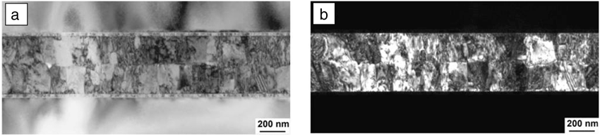
Liu et al. reported that Cu-to-Cu direct bonding can be accomplished below 200°C in ordinary vacuum by using highly (111)-oriented Cu, in which almost 100% of the surface area is (111) oriented.Reference Liu, Lin, Chu, Chen, Lyu, Chen and Tu52Figure 7a presents a cross-sectional transmission electron microscopy (TEM) image of a bonded Cu film after bonding at 150°C for 1 h.Reference Liu, Lin, Chu, Chen, Lyu, Chen and Tu52 The dark-field TEM image shown in Figure 7b indicates that the bonding surfaces are all (111) oriented. An excellent interface can be obtained because the surface diffusion coefficient on the (111) surface of Cu is three to four orders of magnitude faster than on other surfaces.Reference Agrawal, Rice and Thompson53 Hsiao et al. reported that nanotwinned Cu prepared by electroplating also possesses a preference for high (111) orientation.Reference Hsiao, Liu, Lin, Liu, Lu, Huang, Chen and Tu54 Therefore, the nanotwinned Cu films may also be adopted to achieve low temperature Cu-to-Cu direct bonding. Nevertheless, more effort is needed for the implementation of Cu direct bonding as 3D IC vertical interconnects.
Bonding between two sputtered (111) Cu films at 150°C for 1 h. (a) Bright-field transmission electron microscope (TEM) image of two (111) nanotwinned Cu films after bonding. (b) Dark-field TEM image of the Cu films, indicating the grains are (111) oriented.Reference Liu, Lin, Chu, Chen, Lyu, Chen and Tu52
Conclusion
This article reviewed the status of current research on vertical interconnects using microbumps. Several critical reliability issues, such as transformation of solder joints into IMC joints, necking or voiding induced by side wetting/diffusion on the circumference of UBM, formation of porous Cu3Sn IMCs, early electromigration failure caused by specific orientations of Sn grains, and precipitation of plate-like Ag3Sn IMCs were discussed. These issues are mainly caused by the small volume of solder in the microbump. More efforts are needed to better understand these issues and provide solutions to these problems. Even though the issues for the 20 μm microbumps can be solved, the dimension of the microbumps will continue to scale down. The diameter of the microbumps is expected to shrink to 10 μm in five years. Therefore, these issues may emerge again and need to be examined in smaller microbumps.
Acknowledgments
Financial support from the Ministry of Science and Technology, Taiwan, under contract 101–2628-E-009-017-MY3 is acknowledged.