Introduction
Phase-change materials (PCMs) have attracted significant interest in the last few years. There are two major reasons for this attention. PCMs have a wide range of present and potential applications, ranging from rewriteable optical data storage to novel electronic memories and switchable photonic devices.Reference Lencer, Salinga, Grabowski, Hickel, Neugebauer and Wuttig1–Reference Raoux, Wełnic and Ielmini3 For these applications, it is crucial to understand the source of the unconventional properties of PCMs,Reference Raty, Schumacher, Golub, Deringer, Gatti and Wuttig4,Reference Wuttig, Deringer, Gonze, Bichara and Raty5 and how the properties can be tailored. Yet, PCMs are also stimulating from the perspective of fundamental sciences. What are the origins of the unconventional properties that characterize these remarkable solids? In this article, we attempt to address both perspectives.
We first summarize the properties portfolio that is desirable for different applications of PCMs, in particular, where improvements of materials properties promise significant gains in the application arena. Subsequently, we briefly address how material properties can be explained utilizing fundamental concepts of the relationship between bonding, structure, and properties. The emerging insights are then employed to address an aspect of significant application interest—the origin of the high switching speeds.Reference Makino, Tominaga and Hase6,Reference Wełnic and Wuttig7 Finally, the potential of the approach presented is critically evaluated.
PCMs and switching speeds
PCMs are presently employed for rewritable optical and electronic data storage. Both means of storage utilize the fact that PCMs can exist at room temperature in both a metastable amorphous phase and a (more stable) crystalline state.Reference Kolobov, Fons and Tominaga8 The coexistence of two such states can be realized in many materials, including Si and SiO2 (glass and crystal). What makes PCMs stand out are the potentially high switching speeds from the amorphous to the crystalline state at elevated temperatures, which can be as short as 1 ns, or less,Reference Loke, Lee, Wang, Shi, Zhao, Yeo, Chong and Elliott9–Reference Bruns, Merkelbach, Schlockermann, Salinga, Wuttig, Happ, Philipp and Kund11 while the amorphous phase can be stable for more than 10 years at room temperature. The switching speed exhibits an extraordinary temperature dependence in these materials, with an increase in temperature of about 300 K leading to an increase in switching speed by 16–17 orders of magnitude.
The second highly remarkable feature of this material class is the pronounced difference in properties between the amorphous and the crystalline states. While the optical properties of SiO2 such as the optical reflectivity hardly differ in the amorphous (glassy) and crystalline states. This is very different for PCMs, where the amorphous and crystalline phase show a pronounced difference in refractive index and optical polarizability ε∞, leading to applications such as their use in Blu-ray discs.Reference Wuttig and Yamada2
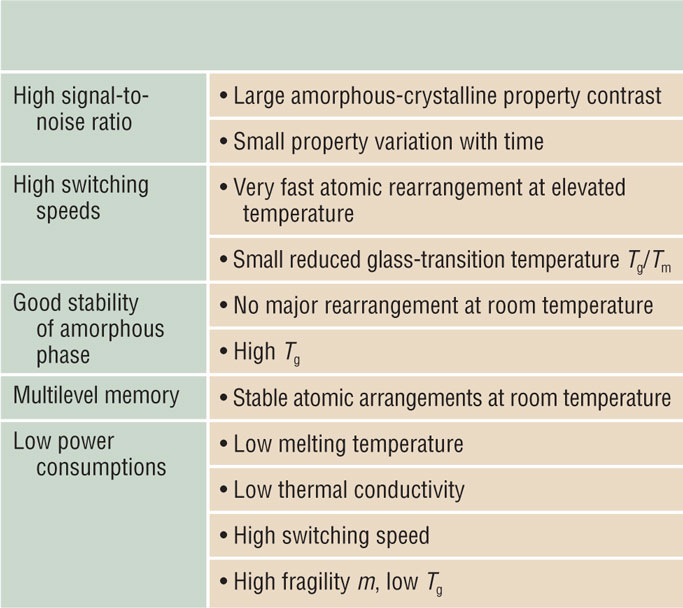
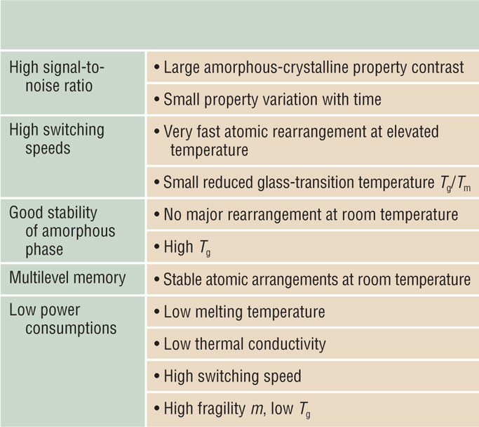
The requirements listed in Table I for PCMs in data-storage applications are closely interwoven with material properties, such as the atomic arrangement and its stability, the speed of crystallization and atomic relaxation processes, as well as the consequences of differences in atomic arrangement between the amorphous and crystalline states on switching speed and the contrast in their properties.
Requirements for phase-change materials in data-storage applications.
A number of approaches have been conducted over the last decade to explain the unusual properties of PCMs. One line of inquiry has focused on the atomic arrangement in the amorphous phase. The rationale behind this approach is that both the switching speed and the property contrast can potentially be attributed to differences in the atomic arrangements in the two phases. Indeed, these studies have provided interesting insights, addressing for example, the role of Ge in the structure of amorphous Ge2Sb2Te5Reference Kolobov, Fons, Frenkel, Ankudinov, Tominaga and Uruga12 and the importance of the distortion away from a perfectly octahedral atomic arrangement.Reference Huang and Robertson13 Yet, it has been difficult to derive insights into how novel PCMs could be found or how property trends can be predicted. Which prompted the question: is there an alternative approach?
Unconventional properties of PCMs
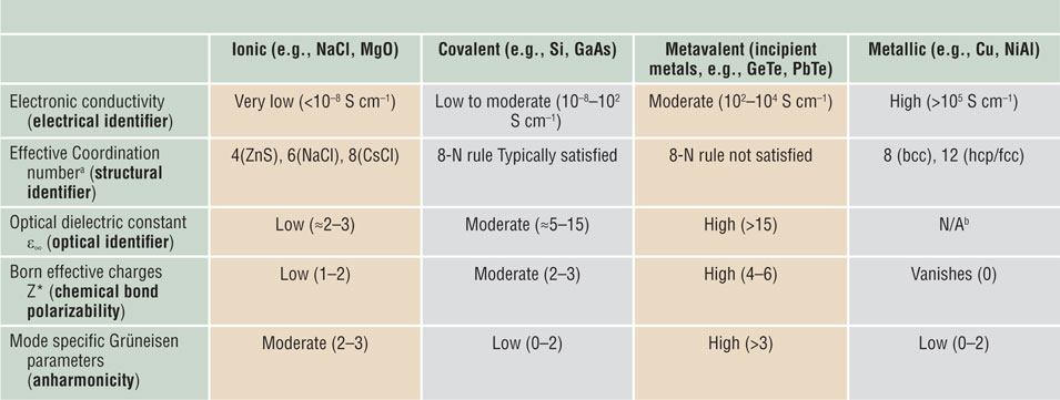
If the chalcogenides used as PCMs such as GeTe or Ge2Sb2Te5 have so many interesting applications, this might be attributed to the fact that they possess a combination of unconventional properties.Reference Wuttig, Deringer, Gonze, Bichara and Raty5 This is indeed the case, as summarized in Table II, which compares the characteristic property portfolio of materials employing ionic, metallic, or covalent bonding and relates these properties to the property portfolio characteristics for chalcogenides such as GeTe, Ge2Sb2Te5, PbTe, or Bi2Se3. This comparison reveals that these chalcogenides show rather unconventional properties. They have electrical conductivities between those of metals and covalently bonded solids. In addition, crystalline PCMs such as SnTe, GeTe, or Ge2Sb2Te5 are characterized by high values of the optical dielectric constant ε∞.Reference Wuttig, Deringer, Gonze, Bichara and Raty5 Their effective coordination number (ECoN) is incompatible with the 8-N rule, where N is the number of outer shell electrons or group number, which is usually obeyed for covalently bonded materials (e.g., Group IV element Si features four nearest neighbors). Hence, in SnTe, the Sn and Te atoms should on average have three nearest neighbors. Instead, the effective coordination number is closer to six, signaling a significant deviation from ordinary covalent bonding. Furthermore, these crystalline phases possess high values of the Born effective charge Z*, a measure of the chemical bond polarizability.
Property-based “fingerprints” to define bonding in inorganic materials.
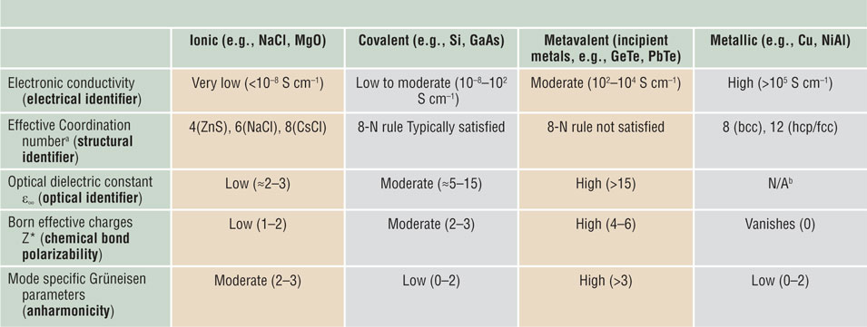
The fingerprint for metavalent solids is a combination of five different identifiers, all of which need to be present in a given material (e.g., NaCl and PbTe have the same structural identifier, but the electronic conductivity in NaCl is extremely low).Reference Wuttig, Deringer, Gonze, Bichara and Raty5
+a For ionic and metallic systems, representative structure types are given, but there are many others especially for multinary systems (e.g., in Zintl phases). b This indicator is not normally applicable to the metallic state.
Finally, these materials are characterized by high values of the Grüneisen parameter for the transverse optical modes, γTO; a sign of anharmonic behavior, which describes how much phonon frequencies change with changing volume. Thus, a linear combination of properties typical for other bonding mechanisms (metallic and covalent) is unable to describe the properties for PCMs such as GeTe, PbTe, or others. This can be seen, for example, by a comparison of the typical values of the Grüneisen parameter, γTO. It is high for materials such as GeTe or PbTe, while metallic and covalently bonded materials both generically show low values of γTO. Therefore, bonding in GeTe cannot be considered a bonding just at the boundary between covalent and metallic bonding. Instead, the bonding in GeTe or PbTe should be considered as a unique and novel bonding mechanism, distinctively different from covalent and metallic bonding. Nevertheless, this bonding mechanism seems to be related to both metallic and covalent bonding and has been coined metavalent; the materials that utilize this bonding mechanism have been named incipient metals.Reference Wuttig, Deringer, Gonze, Bichara and Raty5
Bonding and material properties
It might seem bold to link a unique property portfolio to a unique bonding mechanism, but chemical bonding is at its best if it is employed to explain material properties. Nevertheless, it would be highly desirable to obtain further support and confirmation for the notion that there is a novel bonding mechanism in solids besides ionic, metallic, and covalent bonding, yet different from the weaker hydrogen and van der Waals bonding.
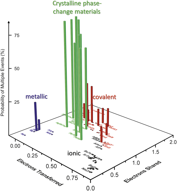
Indeed, such support was obtained by studies of various solids employing atom probe tomography (APT), which has been recently used to analyze PCMs.Reference Zhu, Cojocaru-Mirédin, Mio, Keutgen, Küpers, Yu, Cho, Dronskowski and Wuttig14 These studies have helped not only to detect the exact composition at the nanometer levelReference Cojocaru-Mirédin, Hollermann, Mio, Wang and Wuttig15,Reference Shen, Lv, Chen, Li, Zhang, Song and Zhu16 in the bulk and grain boundaries (a signature for layer intermixing in the case of interfacial phase-change materials), but also to discover surprising behavior in bond rupture during the APT experiments. This was observed when various classes of materials, including covalent, ionic, metallic, and metavalent materials were investigated by APT. The difference in bond rupture is reflected in the probability of multiple events (PMEs) in APT experiments, as summarized in Figure 1.Reference Zhu, Cojocaru-Mirédin, Mio, Keutgen, Küpers, Yu, Cho, Dronskowski and Wuttig14 The PME is defined as the probability of dislodging more than one ion when a laser pulse is applied to the apex of a needle-shape specimen, and expected to be generally very low for most materials.
A 3D map using the basal plane of electrons transferred and electrons shared between atoms in various materials and, in the vertical axis, the “probability of multiple events” (PMEs) measured by laser-assisted atom probe tomography. The coordinates of the basal plane are the degree of electron transfer and electron pair formation between atoms in each material. All compounds with a high probability of generating multiple ionization events upon exposure to a single laser pulse are located in the green area of this plot, which is characterized by unconventional physical properties. In the green region, the PMEs range from about 60% to more than 80%, while the highest value observed outside this region is about 33%. This is thus clear experimental proof that the bond-breaking behavior of the crystalline phase-change materials differs from materials employing conventional bonding mechanisms (covalent, metallic, and ionic).Reference Zhu, Cojocaru-Mirédin, Mio, Keutgen, Küpers, Yu, Cho, Dronskowski and Wuttig14 The number of electrons transferred is adapted from Reference Reference Raty, Schumacher, Golub, Deringer, Gatti and Wuttig4, but renormalized by the formal oxidation state.
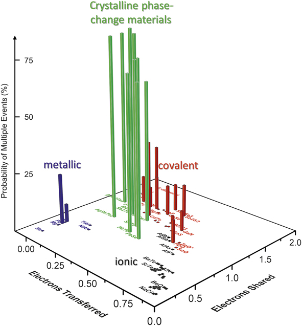
Yet, Figure 1 shows that for those materials characterized by an unconventional combination of properties (PCMs), such as high dielectric constant ε∞, large Born effective charge Z*, high effective coordination number ECoN, and large Grüneisen parameter γTO, a high PME (>60%) is observed. On the contrary, for all other materials that utilize covalent, ionic, or metallic bonding, a low PME (<33%) was detected, in agreement with the value expected and observed when a standard coevaporation phenomenon takes place in APT.Reference De Geuser, Gault, Bostel and Vurpillot17 The exceptionally high PMEs observed in the former are hence an intrinsic property of crystalline PCMs. The mechanism responsible for this behavior was termed enhanced correlated field evaporation,Reference Zhu, Cojocaru-Mirédin, Mio, Keutgen, Küpers, Yu, Cho, Dronskowski and Wuttig14 and should not be mistaken for the high PME of approximatively 40–45% detected when either field dissociation of molecular ionsReference Saxey18,Reference Gault, Saxey, Ashton, Sinnott, Chiaramonti, Moody and Schreiber19 or known measurement artifactsReference Tang, Gault, Ringer and Cairney20,Reference Thuvander, Kvist, Johnson, Weidow and Andrén21 occur.
Bonding in solids
So far, we have characterized materials and the bonding mechanism they utilize by their properties and their bond-breaking behavior. At the same time, other bond descriptors have been developed based on the quantum theory of atoms in molecules and crystals.Reference Gatti22 Two quantities are frequently utilized to characterize the nature of the chemical bond, the number of electrons transferred to/from an atom and the number of electrons shared between neighboring atoms. The amount of electrons shared between adjacent atoms (ES) and the number of electrons transferred to an atom (ET) can be used to distinguish between ionic, metallic, and covalent bondsReference Raty, Schumacher, Golub, Deringer, Gatti and Wuttig4 (e.g., purely covalent bonding features only shared electrons and no transferred electrons, while the opposite is true for the ionic bond). The ES and ET values are calculated from the difference in the electron wave function between the single atoms and the compound, as described in Reference Reference Raty, Schumacher, Golub, Deringer, Gatti and Wuttig4. Employing ES and ET values as coordinates in a plot, metals, ionic, and covalent compounds as well as incipient metals cluster in groups (i.e., occupy different regions) in this plot (see Figure 2). In this map, crystalline PCMs such as GeTe or Sb2Te3 are situated in between typical metallic and covalent materials. Yet, their properties are different (Table II) and feature a very different bond-breaking behavior (Figure 1).
Two-dimensional map describing bonding in solids. The map is spanned by electron transfer (ET, ΔQ) between atomic basins (Ωij), and the formation of electron pairs between them (ES), δ(Ω1,Ω2). Triangles, diamonds, squares, and circles denote tetrahedrally bonded solids, distorted and ideal rock-salt-type (octahedrally coordinated) structures, body-centered solids, and close-packed metals, respectively, while filled and open symbols represent thermodynamically stable and metastable phases (vdW, van der Waals).Reference Raty, Schumacher, Golub, Deringer, Gatti and Wuttig4 Phase-change materials such as GeTe or Sb2Te3 all occupy a well-defined region of the map highlighted in green.
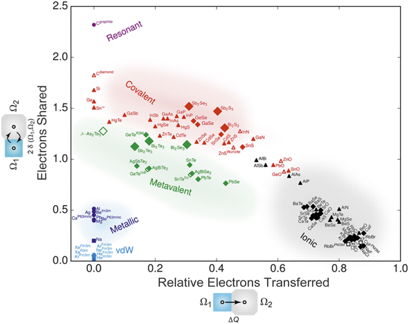
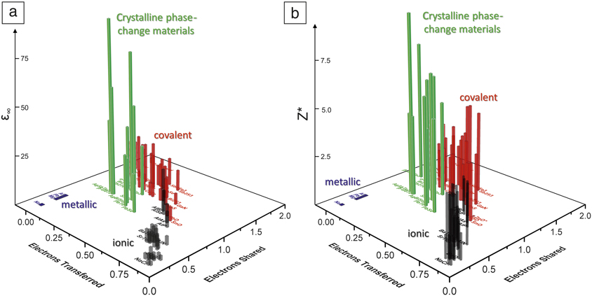
We can use this insight in a number of ways. First, it helps us to identify other materials that should have the desired properties of PCMs. Similar maps can also be utilized to understand property trends, such as trends for ε∞ or Z*. This is demonstrated in Figure 3, where both quantities are shown.
Three-dimensional maps showing unconventional properties of crystalline phase-change materials (in green) as compared with other classes of materials (covalent in red, metallic in blue, and ionic in black). (a) The optical dielectric constant, ε∞, is plotted against ET and ES. ε∞ is an optical identifier of chemical bonding.Reference Raty, Schumacher, Golub, Deringer, Gatti and Wuttig4,Reference Wuttig, Deringer, Gonze, Bichara and Raty5 (b) The Born effective charge, Z*, is plotted against electrons transferred (ET) and electrons shared (ES). Z* is a signature of the chemical bond polarizability.
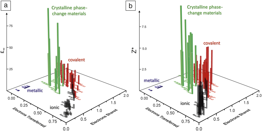
One can see that Z* is particularly large for materials that employ metavalent bonding and lie next to the region of metallic bonding. For ε∞, high values are again found in the same region, but now for smaller values of electron transfer. It is quite interesting to observe such clear property trends as a function of changes in chemical bonding. However, regarding the requirements listed in Table I, neither ε∞ nor Z* provide crucial guidance for property design. In this regard, a quantity such as γTO is more interesting, since it is closely related to the thermal conductivity of the lattice κlat. High values of γTO lead to low values of the thermal conductivity, which helps to ensure that the power consumption upon melting is reduced. The generally low thermal conductivities also help to understand why many materials in the region of metavalently bonded materials are also good thermoelectrics.
There are other properties that are potentially more important for PCMs. As can be seen from Table I, a crucial attribute of PCMs is their ability to be rapidly switched. Since crystallization of a PCM memory cell takes longer than melt-quenching,Reference Loke, Lee, Wang, Shi, Zhao, Yeo, Chong and Elliott9 the focus is on how to improve the crystallization speed and the material parameters involved.
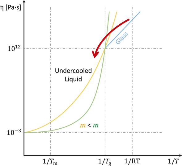
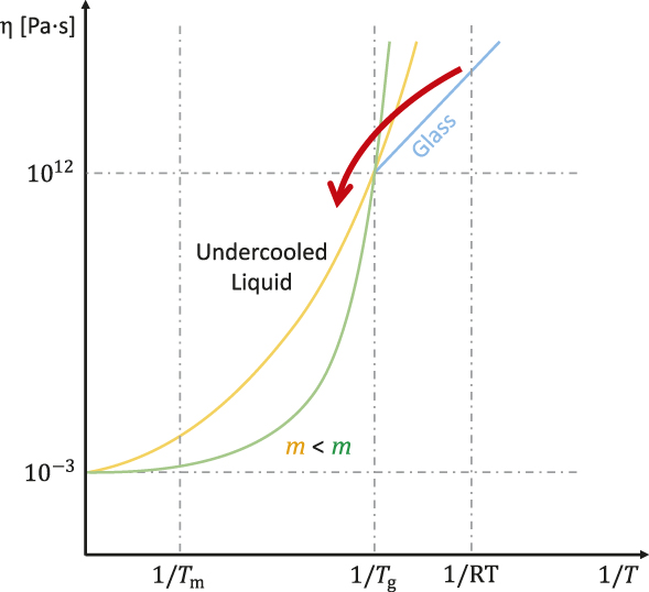
Usually the regime of fast crystallization lies between the glass-transition temperature, T g, and the temperature of melting, T m. For PCM memory devices, it is necessary to enter this regime with minimal energy dissipation. In order to minimize energy dissipation, the absolute value of the glass-transition temperature, T g, and the melting temperature, T m, should be low. However, when the glass-transition temperature is too low (close to room or operating temperature), slight variations in temperature could lead to an unintended crystallization and reduced data retention times. On the other hand, when the glass-transition temperature is too high, too much energy will be required for achieving the temperatures needed for rapid crystallization. Additionally, the reduced glass transition, T g/T m, should be small for rapid crystallization.Reference Turnbull23 When the glass transition and reduced glass-transition temperature meet these criteria, the fragility, m, of the material should be as high as possible. A high fragility of an undercooled liquid (UCL) is related to bad glass-forming ability and is characterized by a tremendous decrease in viscosity, η, upon the transition from a glass into the UCL, as depicted in Figure 4 (see the Wei et al. article in this issue for more information).Reference Gulbiten, Mauro, Guo and Boratav24–Reference Wei, Lucas and Angell26 Since the crystal growth velocity and nucleation rate are inversely related to viscosity η,Reference Turnbull23–Reference Orava and Greer30 these increase hugely when the temperature exceeds the glass-transition temperature for high-fragility materials. Thereby, the necessary temperature increase for rapid crystallization and the energy required, as well as the time for complete crystallization, are reduced further by high fragility. Hence, it would be highly desirable to explore systematic trends for T g, T g/T m, and fragility, m, as a function of chemical bonding in a map (Figure 3).
Schematic sketch of viscosity, η, as a function of inverse temperature (Angell plot). When a glass is heated from room temperature (RT) to above the glass-transition temperature, T g, it enters the undercooled liquid phase. Upon glass transition, the temperature dependence of viscosity experiences a discontinuity.Reference Gulbiten, Mauro, Guo and Boratav24 When heated further to exceed the glass transition, the viscosity, η, decreases faster at higher fragility, m.Reference Martinez and Angell25 Since the crystal growth velocity and nucleation rate are both inversely proportional to viscosity, η, a more fragile material should crystallize faster than a less fragile one.
The glass-transition temperature is often determined in calorimetric experiments, where in the case of PCMs, crystallization initiates before the glass transition is revealed.Reference Kalb, Wuttig and Spaepen31 Because of this, T g can only be estimated, which leads to a wide spread of reported T g values ranging from 100 to 200°C in the case of the prominent PCM Ge2Sb2Te5.Reference Sebastian, Le Gallo and Krebs27,Reference Orava, Greer, Gholipour, Hewak and Smith28,Reference Kalb, Wuttig and Spaepen31–Reference Chen, ten Brink, Palasantzas and Kooi34 For another prominent PCM, AIST (AgInSbTe), values ranging from 105 to 185°C are reported.Reference Kalb, Wuttig and Spaepen31,Reference Lankhorst32,Reference Zalden, von Hoegen, Landreman, Wuttig and Lindenberg35–Reference Orava, Hewak and Greer37 However, in order to precisely predict crystallization kinetics of PCMs, accurate and physically meaningful values for T g are mandatory. Until the development of suitable techniques to obtain these values experimentally, the range of possible T g values can be restricted only due to the combined knowledge of its crystallization kinetics, glass dynamics, microscopic behavior, and by additional supportive simulations.Reference Pries, Wei, Wuttig and Lucas38
A similar situation is present for assigning fragility values to PCMs. Since PCMs crystallize readily, the time scale to observe the UCL for measuring the viscosity is limited. For this reason, viscosity data, if any, only exist above or close to the melting temperature, T m, but not close to the glass-transition temperature, T g, where the fragility is usually determined. This lack of viscosity data in between T g and T m is truly a limitation for predicting the inversely proportional crystal growth velocity.
Summary
Besides being used in memory applications today, PCMs still offer the opportunity of further technological advances as well as exciting fundamental scientific insights. The unique bond breaking behavior observed in atom probe tomography is indicative of a novel bonding mechanism. This mechanism partly resembles metallic or covalent bonding, and yet PCMs feature a portfolio of properties which is not a linear superposition of metallic and covalent bonding. The maps described in this article, in which bonding character is clearly linked to trends in material properties, constitute a useful new route in material engineering. Unfortunately, so far it has not been possible to extend this map to crystallization kinetics, in order to tailor switching speeds of PCMs. The values reported so far for the glass-transition temperature of PCMs are inconclusive and contradictory. In addition, there are significant difficulties in determining the fragility of these materials. Hence, it has not yet been possible to produce a figure such as Figure 1 or Figure 3, where either T g, T g/T m, or fragility values are depicted as a function of chemical bonding parameters (i.e., ES and ET). However, as such data become available, they will provide a framework to understand and optimize switching speeds and hence possibly provide an intriguing approach to tailor PCMs.

Julian Pries is a doctoral candidate at RWTH Aachen University, Germany, where he obtained his master’s degree in physics. His current research focuses on glass dynamics and crystallization kinetics of phase-change materials. Pries can be reached by email at pries@physik.rwth-aachen.de.

Oana Cojocaru-Mirédin has led the Nanocharacterization of Advanced Functional Materials Group in the Institute of Physics at RWTH Aachen University, Germany, since 2015. She received her PhD degree in physics in 2009 from the University of Rouen, France. She completed postdoctoral research at the Max-Planck-Institut für Eisenforschung, Germany. In 2013, she became the head of the Interface Design in Solar Cells Group at Max-Planck-Institut für Eisenforschung. Her research interests include the characterization and processing of compound semiconductors for energy and microelectronic applications by means of correlative microscopy. She has more than 60 peer-reviewed articles and contributions in 40 conferences. Cojocaru-Mirédin can be reached by email at cojocaru-miredin@physik.rwth-aachen.de.

Matthias Wuttig has been a full professor at RWTH Aachen University, Germany, since 1997. Since 2011, he has been the head of a collaborative research center on resistively switching chalcogenides. He received his PhD degree in physics in 1988 from RWTH Aachen/Forschungszentrum Jülich, Germany. He was a visiting scientist/professor at several institutions, including Bell Labs, Murray Hill, Lawrence Berkeley National Laboratory, Stanford University, Hangzhou University, China, IBM Almaden, DSI, Singapore, CiNAM, France, and the Chinese Academy of Sciences. In 2013, he received a European Research Council Advanced Grant to realize novel functionalities by disorder control. His research focuses on the design of novel functional materials. He has approximately 330 publications (∼17,000 citations). In 2019, he was selected as a Materials Research Society Fellow. Wuttig can be reached by email at wuttig@phyik.rwth-aachen.de.