
I. INTRODUCTION
As today’s photovoltaic market continues to be dominated by crystalline silicon (c-Si) technology, two cost-reduction efforts are being contemplated: thinner silicon wafers (<50 µm) and the use of novel materials deposited at low temperatures with high throughput processes. Maximization of the solar cell open-circuit voltage (V OC) to record values of 750 mV Reference Taguchi, Yano, Tohoda, Matsuyama, Nakamura, Nishiwaki, Fujita and Maruyama1 has been possible by combining two principles of c-Si solar cell design Reference Battaglia, Cuevas and De Wolf2 : (i) passivation of surface dangling bonds using hydrogenated amorphous silicon (a-Si:H) or other dielectrics (SiO2, Al2O3, Si3N4, SiC); and (ii) carrier selectivity via electron- and hole-selective contacts, traditionally achieved by phosphorous/boron doping gradients. Eventually, the ideal and simplest strategy would require a passivating/selective contact, dual-functionality materials that effectively passivate the c-Si surface while selectively conduct a specific charge carrier. Reference Cuevas, Allen and Bullock3,Reference Melskens, van de Loo, Macco, Vos, Palmans, Smit and Kessels4
In parallel, thin-film photovoltaics including organic and perovskite solar cells, have introduced a wide variety of electron- and hole-selective materials whose optoelectronic properties are comparable or superior to the standard p- and n-doped layers used in c-Si. Such materials have been successfully applied to c-Si heterojunction devices including organics, Reference Zielke, Pazidis, Werner and Schmidt5 alkali salts, Reference Xu, Yu, Zuo and Yang6,Reference Wan, Samundsett, Bullock, Allen, Hettick, Yan, Zheng, Zhang, Cui, McKeon, Javey and Cuevas7 and transition metal oxides (TMOs), Reference Um, Kim, Lee, Hwang, Seo and Seo8–Reference Yang, Bi, Ali, Davis, Schoenfeld and Weber18 using either low temperature (T < 200 °C) or solution-based processes. In particular, TMOs offer themselves as excellent candidates to substitute traditional c-Si doped layers given their wide range of work function values (3–7 eV), large energy band gaps E gap > 3 eV (high transparency), and marked p- or n-type semiconductivity. Reference Greiner and Lu19 Additionally, their semi-insulating properties allow for passivation of the c-Si surface without compromising carrier conductivity, although their passivation potential in TMO/c-Si heterojunctions limits experimental V OC values to ∼660 mV Reference Bivour, Temmler, Steinkemper and Hermle11 and implied-V OC values to 678 mV. Reference Gerling, Masmitja, Voz, Ortega, Puigdollers and Alcubilla20 This has prompted the use of a-Si:H passivating interlayers to surpass the 700 mV barrier, as it has been demonstrated by a 725 mV V OC and 22.5% conversion efficiency device with MoO3/a-Si:H hole contacts. Reference Geissbühler, Werner, Martin de Nicolas, Barraud, Hessler-Wyser, Despeisse, Nicolay, Tomasi, Niesen, De Wolf and Ballif21 Therefore, a detailed understanding of the surface passivation mechanisms occurring at the TMO/c-Si interface (either by chemical bonding, charge selectivity or both) is still needed to potentiate the use of these passivating/selective materials.
In this work we will study the origin of passivation in three TMO/n-type c-Si (n-Si) heterojunctions, with molybdenum trioxide (MoO3), tungsten trioxide (WO3), and vanadium pentoxide (V2O5) deposited by vacuum thermal evaporation. A detailed characterization of the heterojunction interface will determine two contributions to c-Si surface passivation: (i) through chemical reaction between c-Si and TMOs; and (ii) by carrier-concentration gradients established during Fermi level alignment under equilibrium.
II. EXPERIMENTAL
Sample structures were fabricated on polished float-zone n-type c-Si wafers (100 orientation) with a thickness of 280 μm and 2.5 Ω-cm resistivity. After RCA standard cleaning, wafers were dipped in 1% HF during 1 min to etch SiO2 away. In this step, the surface Si atoms become bonded to hydrogen to form a continuous H-terminated surface. Unfortunately, this configuration is unstable and will be substituted by an ultra-thin native SiO2 layer after only a few hours. Reference DeBenedetti and Chabal22 Therefore, HF-cleaned wafers were transferred into a N2 glovebox to avoid air exposure. Three kinds of test structures were fabricated: (i) symmetric TMO/n-Si/TMO samples (20 nm TMO thickness) for carrier lifetime measurements via the Quasi-Steady-State Photo-Conductance (QSSPC) technique (Sinton WCT-120); (ii) TMO (20 nm)/n-Si samples contacted with Au contacts (50 nm thickness, 10 × 0.27 mm2 contact area) in a Transmission-Line-Method (TLM) array for contact resistivity measurements Reference Bullock, Cuevas, Allen and Battaglia23 ; and (iii) ITO (Indium Tin Oxide)/TMO/n-Si samples for detailed characterization of the material interfaces. The three transition metal oxides, MoO3, WO3, and V2O5 (powdered 99.99%, Sigma Aldrich) were thermally evaporated under vacuum (<8 × 10⁻⁶ mbar) from a tantalum boat for thicknesses in the 10–70 nm range at a 0.2 Å/s rate, which was monitored by quartz crystal micro-balance. During the evaporation process, heating of the Si substrate was negligible and remained at ambient temperature. ITO films (70 nm) were deposited on TMO/n-Si after a brief air exposure by RF-magnetron sputtering under an argon partial pressure of 3.5 × 10⁻³ mbar and a power density of 2.5 W/cm2. This ITO layer, which works as a transparent electrode and anti-reflecting layer in a TMO/n-Si solar cell, also protects the air-sensitive TMO layer from degradation and work function changes. Reference Meyer, Hamwi, Kröger, Kowalsky, Riedl and Kahn24
The ITO/TMO/n-Si structures were first characterized by High Resolution Transmission Electron Microscopy (HR-TEM), using lamellas prepared by Focused Ion Beam (FIB) milling with Ga+ ions (NEON40, Carl Zeiss AG, Oberkochen, Germany). Cross-sectional HR-TEM imaging (JEOL 2010F, JEOL Ltd., Tokyo, Japan) was done with a field-emission electron source at 200 kV and lattice resolution. Secondly, Time of Flight Secondary Ion-Mass Spectroscopy (ToF-SIMS) depth profiling (ION-TOF Model IV, Ion-Tof GmbH, Münster, Germany) was performed by sputtering a sampling area of 300 × 300 μm2 with Cs+ ions (1 keV) under high vacuum (3.8 × 10⁻⁸ mbar). The analysis of the negative secondary ions was done with a Bi1+ source (25 keV) and a time resolution of 200 ps. Charge compensation (<20 eV) was applied via electron flooding, given the semi-insulating character of thin-film layers.
For the X-ray Photoelectron Spectroscopy (XPS) scans, separate samples were prepared by thermally evaporating V2O5 films of different thicknesses (1–10 nm) on n-Si substrates (same conditioning as before). After metal oxide evaporation, each sample was transferred from the glovebox into the XPS chamber after a brief air exposure. The XPS analysis (Phoibos 150 detector, SPECS, Berlin, Germany) was performed at 3 × 10⁻⁹ mbar using a nonmonochromatic Al–Kα source (1486.6 eV) and a 90° incidence angle, guaranteeing a probing depth of at least 10 nm. Deconvolution of the core level spectra was done by Gaussian–Lorentzian fittings after Shirley background subtraction, with all binding energies referenced to the C 1s peak (284.8 eV). Percentage atomic concentrations were calculated from the integration of the fitted peak areas, while correction for adventitious carbon C–OH and C–O contamination (<15% atomic C content) was performed when quantifying the oxygen content.
III. RESULTS AND DISCUSSION
Up to now, numerous studies have used MoO3, WO3 and V2O5 as hole-selective contacts in c-Si heterojunction solar cells. Reference Um, Kim, Lee, Hwang, Seo and Seo8–Reference Bullock, Hettick, Geissbühler, Ong, Allen, Sutter-Fella, Chen, Ota, Schaler, De Wolf, Ballif, Cuevas and Javey13,Reference Gerling, Mahato, Morales-Vilches, Masmitja, Ortega, Voz, Alcubilla and Puigdollers16,Reference Geissbühler, Werner, Martin de Nicolas, Barraud, Hessler-Wyser, Despeisse, Nicolay, Tomasi, Niesen, De Wolf and Ballif21,Reference Bullock, Cuevas, Allen and Battaglia23 Depending on the doping character of the c-Si substrate (n- or p-type), these large work function TMOs can form a hole-selective contact via two pathways Reference Bullock, Cuevas, Allen and Battaglia23 : (i) inducing an inversion layer upon n-Si (i.e., a p–n junction), or (ii) inducing an accumulation layer upon p-Si (i.e., a p–p+ contact). In TMO/n-Si heterojunctions, the resistive losses associated to hole transport across the TMO bulk are not excessive (reaching fill-factor values of up to 80.3%), Reference Geissbühler, Werner, Martin de Nicolas, Barraud, Hessler-Wyser, Despeisse, Nicolay, Tomasi, Niesen, De Wolf and Ballif21 despite the poor lateral conductivity of TMOs (10−7 S/cm) and the large valence-band offset. In this sense, it has been suggested that defects states in the bulk of oxygen deficient TMOs (MoO3−x , V2O5−x ) are responsible for carrier transport. Reference Meyer, Hamwi, Kröger, Kowalsky, Riedl and Kahn24
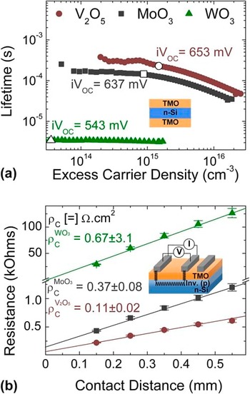
In addition to their transport and selectivity properties, TMOs can also passivate the c-Si surface and decrease carrier recombination, making them excellent candidates as passivating/selective contacts. Both attributes can be observed in Fig. 1(a) depicting the effective lifetime of symmetric TMO/n-Si/TMO test structures, whilst Fig. 1(b) shows the contact resistivity (ρc) extracted from Au/TMO/n-Si structures in a TLM array. The lifetime values at 1 sun illumination (open symbols) are 240, 142, and 4.5 µs for V2O5, MoO3, and WO3 respectively. While these values are in the low range of typical passivated wafers, they translate into implied-V OC values of 653 (V2O5), 637 (MoO3), and 543 mV (WO3), indicating a certain degree of surface passivation. Regarding the TLM measurement, all samples exhibited an ohmic current–voltage response for each contact spacing (not shown), allowing for a precise linear fit to the data (R 2 > 0.99). The extracted ρc values were 0.11 (V2O5), 0.37 (MoO3), and 0.67 Ω-cm2 (WO3), all of which are close to the target series resistance value for most c-Si solar cells (0.1–0.5 Ω-cm2). Note that current flows across the Au/TMO and TMO/n-Si interfaces, including the induced inversion layer on n-Si (see Sec. III. E), so that ρc is the sum of multiple resistance contributions. Reference Bullock, Cuevas, Allen and Battaglia23 Additionally, the sheet resistance of the conduction channel between TLM contacts (extracted from the slope of linear fitting) was 10 (V2O5) and 18 kΩ/sq (MoO3), two orders of magnitude larger than the substrate sheet resistance (∼100 Ω/sq), confirming that carrier transport is confined (at least partially) to the inversion layer. Nonetheless, since passivation of the c-Si surface is not optimal, recombination losses decrease the selectivity for holes and increase ρc, making the TLM analysis somewhat limited. With these results in mind, we now focus on the detailed analysis of the interface and the passivation and transport mechanisms of TMO/n-Si heterojunctions.
(a) Effective carrier lifetime of TMO/n-Si/TMO structures. Open symbols show implied-V OC values at 1 sun illumination intensity. (b) Contact resistivity (ρc) of Au/TMO/n-Si structures extracted from the ohmic current–voltage response in a TLM array. All three TMO thicknesses are 20 nm.

A. Interlayer in TMO/c-Si interfaces
As a first characterization approach, detailed imaging of the fabricated ITO/TMO/n-Si structures was performed by HR-TEM, revealing the presence of an unknown 1.9–2.8 nm thick interfacial layer between the TMOs and the HF-cleaned (and therefore SiO2 free) c-Si surface, as seen in Fig. 2(a). This interlayer (IL), amorphous in nature, is clearly distinguished at the lowest magnifications because of its high contrast to the adjacent materials. Its thickness varies among the three TMOs [Figs. 2(b)–2(d)] but is relatively uniform and without pinholes. Moreover, its shows an abrupt interface with c-Si and a slightly diffused one with the oxides. The maximum IL thicknesses are ∼2.8 nm (WO3), ∼2.5 nm (MoO3), and ∼2.2 nm (V2O5), all of which are greater than the threshold for charge carrier tunneling (∼2.0 nm), Reference Schewchun, Singh and Green25 suggesting that another charge conduction mechanism could be present.
HR-TEM images of the ITO/TMO/n-Si heterostructures showing an interlayer between n-Si and (a and b) MoO3, (c) WO3 and (d) V2O5.

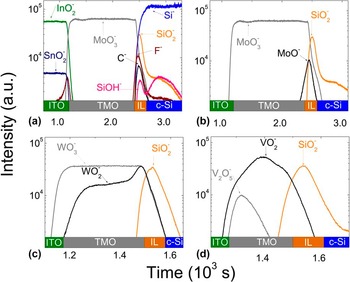
Next, the interlayer composition was qualitatively determined by ToF-SIMS. Figure 3(a) shows the global depth profile of the ITO/MoO3/n-Si sample, where the three distinct materials are clearly differentiated by their respective ions InO2 −/SnO2 −, MoO3 −, and Si−. Extraneous elements including carbon and fluoride (C−, F−) are observed at the material interfaces, related to organic contamination during air exposure and to the HF dips respectively. By increasing the resolution of the time scale [Fig. 3(b)], a signal with an atomic mass unit (amu) of 59.97 and a peak intensity of 3 × 10⁴ counts is observed in the MoO3/n-Si interface, corresponding to SiO2 − ions. Since the HF-cleaned silicon surface is free of any native oxide (as it will be later confirmed by XPS), the presence of SiO2 − ions suggests that a thin silicon oxide IL has formed during thermal evaporation of MoO3, proving that chemical passivation of dangling bonds by oxidation of the silicon surface actually occurs. Within the same time window, a reduced Mo2+ oxide (MoO−) signal is detected, indicating it is a by-product of the oxidation of the Si surface by MoO3 (Si + MoO3 → SiO2 + MoO). Since remnants of the HF etch are also observed in the same time window, it can be confirmed that such interlayer is restricted to the TMO/n-Si interface. A compound SiO2–MoO3 signal was also detected at <102 counts, two orders of magnitude lower than the SiO2 signal and following the same trend, indicating that Mo x (SiO y ) silicates could also be present in the IL but at very low concentrations. Finally, a SiOH− ion signal 10 times weaker than SiO2 and following the same trend is also detected, suggesting that both are related and cannot be distinguished from each other. Reference Kanyal, Jensen, Zhu and Linford26
ToF-SIMS depth profile for the ITO/TMO/n-Si heterostructures showing a SiO2 − signal at the interface between n-Si and (a and b) MoO3, (c) WO3 and (d) V2O5. For each TMO, related reduced species (MoO−, WO2 −, VO2 −) are also detected near the interface.

Similarly, the silicon oxide peak is also detected in the WO3/n-Si and V2O5/n-Si interfaces in Figs. 3(c) and 3(d), at similar intensities and associated with reduced TMO species located adjacent to the interface (WO2, V2O4). For vanadium oxide in particular, the reduction reaction extends over the thin V2Ox layer and VO2 − species surpass V2O5 − in intensity. Moreover, since the SiO2 − peak intensities are about the same order of magnitude as their respective TMO signals (3–6 × 10⁴ counts), we can conclude that the oxidation of the surface is complete, in agreement with the TEM images. Finally, SiOH− and silicate signals were also detected in the WO3 and V2O5 samples but at the low intensities mentioned before, leading to the same conclusions.
With respect to the abundant presence of the F− ions (1.0 × 10⁴ counts) and its effect on the interface, a separate V2O5 sample was washed with abundant deionized water after the HF dip. ToF-SIMS showed a decrease of the F− intensity by a factor of 2 (not shown) while the SiO2 − signal remained unchanged. Since Si–F terminations are not kinetically viable during HF etching, it is probable that these F− are only physisorbed. Reference DeBenedetti and Chabal22 However, residual fluorine could also be chemically bonded to Si, providing additional dangling bond passivation both to the c-Si surface and the SiO x interlayer. Reference Weinberger, Peterson, Eschrich and Krasinski27
B. Thermodynamic feasibility
The formation of a SiO2 layer on a H-terminated Si surface could be explained by chemical reaction with TMOs during deposition. The growth of SiO x interlayers on c-Si has been previously reported for dielectric oxides such as Al2O3, HfO2, Ta2O5, LaAlO3, and SrTiO3, with interlayers varying in stoichiometry (SiO x , Hf1−x Si x O2) and in thickness (0.7–9 nm). Reference Wilk, Wallace and Anthony28–Reference Li, Xiang, Lu and Mai30 This is partially explained by the high reactivity of H-terminated Si, Reference DeBenedetti and Chabal22 but also from purely thermodynamic considerations. Parting from the oxidation of Si and V by molecular O2, the feasibility of these reactions is given by their negative Gibbs formation energies (ΔG):
 $${5 \mathord{\left/ {\vphantom {5 2}} \right. \kern-\nulldelimiterspace} 2}{\rm{Si}} + {5 \mathord{\left/ {\vphantom {5 2}} \right. \kern-\nulldelimiterspace} 2}{{\rm{O}}_2} \to {5 \mathord{\left/ {\vphantom {5 2}} \right. \kern-\nulldelimiterspace} 2}{\rm{Si}}{{\rm{O}}_2}\quad \Delta {G_{{\rm{Si}}-{{\rm{O}}_2}}} = - 858\;{{{\rm{kJ}}} \mathord{\left/ {\vphantom {{{\rm{kJ}}} {{\rm{mol}}}}} \right. \kern-\nulldelimiterspace} {{\rm{mol}}}}$$
 $$2{\rm{V}} + {5 \mathord{\left/ {\vphantom {5 2}} \right. \kern-\nulldelimiterspace} 2}{{\rm{O}}_2} \to {{\rm{V}}_2}{{\rm{O}}_5}\quad \Delta {G_{{\rm{V}}-{{\rm{O}}_2}}} = - 573\;{{{\rm{kJ}}} \mathord{\left/ {\vphantom {{{\rm{kJ}}} {{\rm{mol}}}}} \right. \kern-\nulldelimiterspace} {{\rm{mol}}}}$$
For the case where Si is oxidized by V2O5, the vanadium oxidation reaction should be subtracted from the silicon one, leading to:
 $${5 \mathord{\left/ {\vphantom {5 2}} \right. \kern-\nulldelimiterspace} 2}{\rm{Si}} + {{\rm{V}}_2}{{\rm{O}}_5} \to {5 \mathord{\left/ {\vphantom {5 2}} \right. \kern-\nulldelimiterspace} 2}{\rm{Si}}{{\rm{O}}_2} + 2{\rm{V}}\quad \Delta {G_{{\rm{Si}}-{{\rm{V}}_2}{{\rm{O}}_5}}} = \Delta {G_{{\rm{Si}}-{{\rm{O}}_2}}} - \Delta {G_{{\rm{V}}-{{\rm{O}}_2}}} = - 285\;{{{\rm{kJ}}} \mathord{\left/ {\vphantom {{{\rm{kJ}}} {{\rm{mol}}}}} \right. \kern-\nulldelimiterspace} {{\rm{mol}}}}$$
Hence, the oxidation of Si by a metal oxide is thermodynamically feasible (spontaneous) if the resulting Gibbs energy of that reaction is negative. The same condition is met for the rest of the TMOs under study, with
 $\Delta {G_{{\rm{Si}}-{\rm{W}}{{\rm{O}}_3}}} = - 348$
and
 $\Delta {G_{{\rm{Si}}-{\rm{Mo}}{{\rm{O}}_3}}} = - 406\;{\rm{kJ}}/{\rm{mol}}$
, using the standard Gibbs formation energies at 300 K.
Reference Reed31
An exception to this rule is observed for HfO2 and Al2O3 (ΔG positive), indicating that the spontaneity of these reactions is also affected by the initial equilibrium conditions, kinetic rates and the reactivity of the interface. Note also that any oxidation reaction essentially takes place by electron transfer, meaning that an electron (ē) loss in Si yields an oxidized species (Si0 – 2ē → Si2+). Regarding the relative ΔG magnitudes (V2O5 > WO3 > MoO3), no clear correlation was found with IL thickness (Fig. 2). Similarly, a correlation between ΔG and the work function values for air-exposed TMOs (
 ${\phi _{{{\rm{V}}_{\rm{2}}}{{\rm{O}}_{\rm{5}}}}} \sim 5.3$
,
 ${\phi _{{\rm{W}}{{\rm{O}}_{\rm{3}}}}} \sim 5.0$
,
 ${\phi _{{\rm{Mo}}{{\rm{O}}_{\rm{3}}}}} \sim 5.4\;{\rm{eV}}$
)
Reference Gerling, Mahato, Morales-Vilches, Masmitja, Ortega, Voz, Alcubilla and Puigdollers16
was not found, although it cannot be dismissed given that ϕ is very sensitive to surface conditions and literature values vary considerably.
Reference Meyer, Hamwi, Kröger, Kowalsky, Riedl and Kahn24
C. XPS of TMO/interlayer/c-Si region
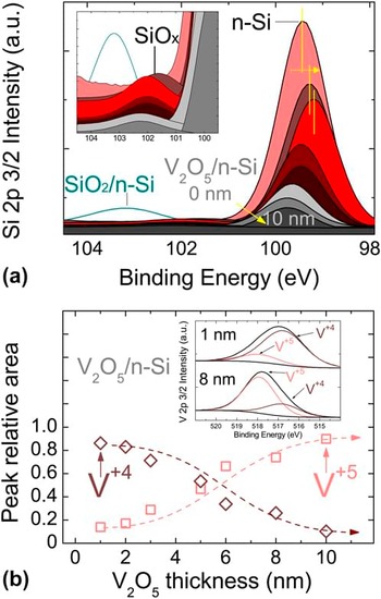
As suggested before, the degree of completion of TMO/n-Si reactions could be less than unity, so that Si would partially oxidize (Si + V2O5 → SiO x + V2O5−x ) and a mixture of sub-stoichiometric species would coexist in the interlayer. Therefore, a detailed chemical composition of the TMO/IL/n-Si interfaces was obtained from XPS analyses of V2O5 films deposited on n-Si at incremental thicknesses (1–10 nm), as a way to monitor film growth and the chemical/electronic changes taking place at the interface. Figure 4(a) shows the Si 2p core level spectra as a function of binding energy, deconvoluted for the Si 2p 3/2 doublet. For the reference case where no V2O5 is present, only one peak centered at 99.4 eV binding energy can be observed, characteristic of the Si0 substrate. Reference Himpsel, McFeely, Taleb-Ibrahimi and Yarmoff32 As soon as 1 nm V2O5 is deposited, an additional chemical state is detected at a higher binding energy of 102.0 ± 0.3 eV [Fig. 4(a) inset] and remains discernible for thicker V2O5 films. This peak, attributed to sub-stoichiometric SiO x∼1.5 species (Si3+), Reference Himpsel, McFeely, Taleb-Ibrahimi and Yarmoff32 is identified as one of the components of the interlayer revealed by HR-TEM and ToF-SIMS. As a reference, a stoichiometric SiO2 oxide grown by wet etching of n-Si with HNO3 is shown with its Si4+ peak at 103.2 eV. The sub-stoichiometry of the SiO x interlayer is relevant to explain why its thickness (as measured by HR-TEM) does not impede the transversal conduction of charge carriers. Instead, a trap-assisted conduction mechanism via defects (oxygen vacancies) might be taking place, not being limited by the maximum tunneling thickness (∼2 nm) of SiO2 passivation layers. Reference Schewchun, Singh and Green25 The atomic Si3+ concentration in the IL was 0.9–2.0% and fairly constant for every sample, suggesting SiO x formation takes place during the first deposition stages until it saturates, remaining constant afterward.
XPS analysis of the V2O5/interlayer/n-Si region for various V2O5 thicknesses (1–10 nm). (a) Si 2p 3/2 doublet spectra showing the characteristic features of the silicon substrate (Si0, 99.4 eV) and a sub-stoichiometric SiO x∼1.5 (Si3+, ∼102.0 eV) attributed to the TMO/n-Si interlayer. As a reference, a stoichiometric SiO2 (Si4+, 103.2 eV) is shown. Inset shows a detailed view of these features. The peak maxima, marked with a vertical line, shifts to lower energies as thickness increases. (b) Evolution of the V4+ and V5+ cation species close to the n-Si interface (dotted lines are a guide to the eye). Inset shows the V 2p 3/2 doublet spectra showing the characteristic features of V4+ (516.8 eV) and V5+ (518.0 eV) states.

Since the Si → SiO x partial oxidation reaction probably implies a complementary V2O5 → V2O5−x partial reduction, the XPS analysis of the vanadium V 2p core level spectra should show the vanadium oxidation states involved. This is depicted in Fig. 4(b) inset where the V 2p 3/2 doublet is deconvoluted into two peaks, corresponding to the V5+ and V4+ cation species. Reference Biesinger, Lau, Gerson and Smart33 The area of each cation provides the relative V4+ and V5+ atomic concentrations as a function of V2O5 film thickness [Fig. 4(b)]. The observed trend is the following: V4+ species, associated with oxygen-deficient films (V2O x<5) and generated by reduction (V5+ → V4+), are primarily found in the vicinity of the SiO x IL and tend to decrease as the V2O5 film thickens; inversely, V5+ species are lowest close to the IL and tend to increase until reaching a relatively fixed concentration in the bulk (away from the interface and its influence). Similar trends have been observed previously for MoO3/metal Reference Greiner, Chai, Helander, Tang and Lu34 and MoO3/n-Si Reference Gerling, Mahato, Voz, Alcubilla and Puigdollers35 systems, where reduced cation states (Mo5+) exist near the interface. The presence of V4+ cations was already expected from the ToF-SIMS depth profiles, where VO2 − ions were detected adjacent to the SiO x interlayer. Therefore, although no detailed XPS analyses were performed with incremental WO3 and MoO3 thicknesses, the similarity between the ToF-SIMS/HR-TEM results indicate that analogue interlayers with SiO x≤2 composition and reduced cation transitions (Mo6+ → Mo5+, W6+ → W5+) can be expected as well, as it has been recently confirmed in the literature. Reference Ding, Boccard, Holman and Bertoni36,Reference Liang, Su, Zhou, Gong, Zhao, Chen, Xie, Zhang, Chen, Liu and Xie37
D. Film stoichiometry and growth mode
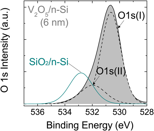
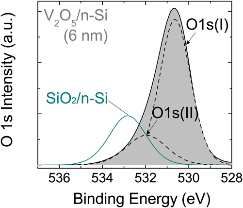
Compared to the qualitative composition obtained from ToF-SIMS, XPS allows the quantification of film stoichiometries in terms of oxygen to metal ratios (O/M). However, the specific distribution of oxygen species (SiO x , V2O x ) from the total oxygen content is not straightforward. To clarify this issue, we focus on the oxygen O 1s XPS spectra shown in Fig. 5 for the V2O5/n-Si region. From the deconvolution of the spectra, two components representing different chemical states are recognized. The first (larger) component is centered at 530.9 ± 0.3 eV, attributed to O in vanadium oxide. Reference Biesinger, Lau, Gerson and Smart33 The second (smaller) component is centered at a higher binding energy (532.3 ± 0.3 eV) and is detected for every V2O5 thickness (1–10 nm), comprising ∼25% of the total O 1s area. This secondary-O, which has been previously described as a defective oxide inherent to many other TMOs, Reference Biesinger, Lau, Gerson and Smart33 has its source on surface hydroxides (V–OH) and adventitious carbon (C–O) physisorbed during exposure to humid air Reference Greiner, Chai, Helander, Tang and Lu34,Reference Greiner, Helander, Bin Wang, Tang and Lu38 when transferred out of the glovebox into the XPS chamber. Additionally, the sub-stoichiometric SiO x of the underlying interlayer also contributes to this secondary-O, as it lies very close to the SiO2 reference (centered at 532.8 eV).
O 1s spectra of the V2O5 (6 nm)/n-Si region. The larger feature (labeled I, 530.6 eV) belongs to V2O5, while the smaller one (labeled II, 532.0 eV) is attributed to the SiO x∼1.5 interlayer and to a defective-oxide associated to adventitious oxygen physisorbed during air exposure. As a reference, the spectra for SiO2 (532.8 eV) is also shown.
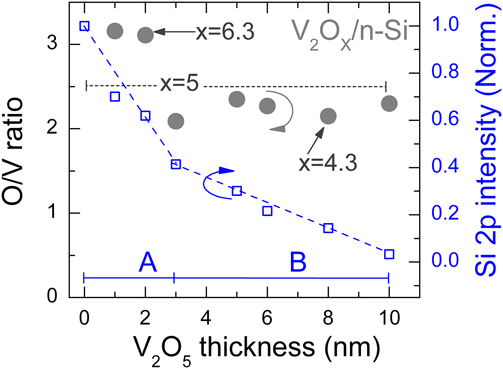
Under these assumptions, the approximate stoichiometry of the V2O5 films can be calculated from the oxygen to metal (O/V) ratios, where O is the total oxygen minus the surface hydroxides, adventitious carbon, and interlayer contributions. Figure 6 (left axis) shows the variation of O/V ratios with film thickness, observing over-stoichiometric ratios O/V >2.5 for the thinnest films (V2O x∼6.3). Considering that other oxygen sources have already been neglected, an excess of oxygen near the interface seems accurate but in conflict with the presence of V4+ cations attributed to oxygen deficient films [Fig. 4(b)]. Such contradiction could be explained by the presence of uncoordinated (dangling) oxygen atoms, an inherent characteristic of TMOs with large stoichiometries (Mo2O6, W2O6 and V2O5) and multi-layered bulk structures, Reference Guo and Robertson39,Reference Hermann, Witko, Druzinic, Chakrabarti, Tepper, Elsner, Gorschlüter, Kuhlenbeck and Freund40 or by the low concentration of silicates detected in the ToF-SIMS analysis. Finally, it is worth mentioning that oxygen vacancies have been reported to be inherent to the bulk of these TMOs (>3 nm), giving rise to defect states deep within the band gap and to its conduction properties. Reference Greiner, Chai, Helander, Tang and Lu34
(Left axis) Evolution of O/V ratios as a function of V2O5 film thickness, indicating a high stoichiometry (V2O x>5) close to the interface. (Right axis) Normalized area of the substrate Si 2p 3/2 peak for each V2O5 thickness, identifying two growth regimes: (A) SiO x interlayer formation and island nucleation of V2O5, and (B) layered growth of V2O5.
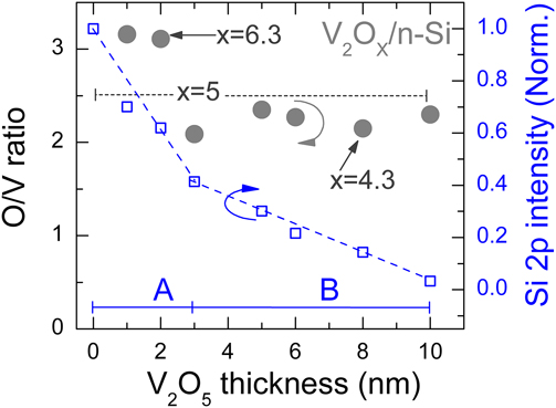
A qualitative measurement of silicon substrate coverage by the deposited TMO can be obtained by plotting the evolution of the Si 2p peak intensity. Figure 6 (right axis) depicts the Si 2p 3/2 peak area, normalized with respect to the maximum value, as a function of V2O5 film thickness. At a first glance, two growth regimes are observed. During the first nanometers, a rapid linear decrease in intensity is observed until a critical thickness is reached, followed by a less steep decline. Given that the IL thicknesses in Fig. 2 are rather uniform, we propose that the first regime (labeled A) is limited by the reaction rate between Si and the metal oxide, followed by V2O5 growth by island nucleation until saturation at ∼3 nm. The second regime (labeled B) is characterized by a monotonic decrease in intensity caused by uniform V2O5 growth on a layer-by-layer basis.
E. Band bending in c-Si and interface dipole
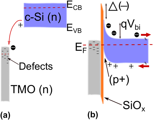
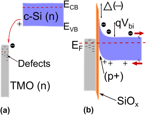
In the previous sections, passivation of the surface dangling bonds by SiO x was proposed as the origin of chemical surface passivation. Nevertheless, the effectiveness of such passivation could be insufficient given that the SiO x film is nonstoichiometric (unpassivated dangling sites remain) and the TMO layer is oxygen-deficient (presence of metal–Si bonds). Therefore, other mechanisms such as field-effect passivation must be present. Figure 7 depicts the proposed energy band diagram for TMO/n-Si before contact (a) and after the formation of the SiO x IL has taken place (b). The TMOs under study tend to induce an inversion (hole-rich) layer on n-Si as a result of their particularly large work functions (ϕTMO > 5.5 eV), forming the selective contact for hole extraction under illumination. Reference Bullock, Cuevas, Allen and Battaglia23,Reference Meyer, Hamwi, Kröger, Kowalsky, Riedl and Kahn24 This transition from n-doping in the Si bulk to p-type character near the surface is a result of the band bending whose magnitude is the built-in potential (V bi) of the heterojunction. Thus, hole selectivity is also established by driving photogenerated electrons away from the anode interface.
Proposed band diagram for the TMO/n-Si heterojunction. (a) Before contact, depicting the transfer of electrons from the valence band (E VB) of n-Si toward the higher work function TMO. (b) After contact, following the formation of a passivating SiO x interlayer. The electron transfer induces a p+ inversion layer on the c-Si surface and possibly a negative dipole Δ(−) until Fermi levels (E F) reach equilibrium.
Evidence of silicon band bending resulting from TMO deposition can be found in the Si 2p core level spectra in Fig. 4(a). A shift of the Si 2p 3/2 peak maximum to lower binding energies is observed as V2O5 is deposited. This shift can be interpreted considering that the difference between the Fermi level (E F) and the valence band (E VB) of n-Si is decreasing, or in other words, up-bending occurs as V2O5 is deposited. Reference Gleason-Rohrer, Brunschwig and Lewis41 A maximum shift of 0.3 eV is obtained for the 2 nm film, although these values are only approximate given the mismatch between the photoelectron sampling depth (<10 nm) and the actual space-charge region width (>100 nm), also being affected by the generated photovoltage from x-ray illumination. Reference Gleason-Rohrer, Brunschwig and Lewis41
The formation of an inversion layer in n-Si by high work function TMOs can be explained as a consequence of Fermi level alignment across the interface. Reference Bisquert42,Reference Wurfel, Cuevas and Wurfel43 Before both materials are contacted, a large electrochemical potential difference exists between them, as defined by the difference in work functions Δϕ = ϕTMO − ϕnSi = 5.4–4.2 eV. Such energy mismatch is the driving force for Fermi level (E F) equilibration. At first, electron transfer from n-Si valence band (E VB ∼ 5.2 eV) into the deep oxygen vacancy (defect) states in TMO is energetically favorable (see Fig. 7). Then, as electrons leave the Si surface, the valence band approaches E F inducing a p+ region. This inversion-effect might be reinforced by negative charges (excess oxygen) fixed in the first V2O x>5 layers, as evidenced by the high O/V ratios. Since band bending cannot occur indefinitely, we presume the n-Si surface reaches a strong inversion condition up to a built-in voltage close to V bi ∼ 0.7 V. At this point, the large Δϕ ∼ 1.2 eV has only been distributed partially in the Si surface, while the remaining energy difference needed for equilibrium is allocated by a negative dipole Δ ∼ −0.5 eV, so that Δϕ = qV bi − Δ. Similar mechanisms have been previously described for TMO/organic semiconductor systems where electron transfer into the TMO results in the formation of interfacial dipoles and p-doping of the organic Highest Occupied Molecular Orbital (HOMO) level. Reference Meyer, Hamwi, Kröger, Kowalsky, Riedl and Kahn24,Reference Irfan, Zhang, Ding, Tang and Gao44 Regarding the location of the dipole, it is probably allocated in the SiO x /n-Si interface, although further characterization (such as impedance analysis) is needed.
IV. CONCLUSIONS
The mechanisms behind the passivation of n-type c-Si surfaces by thin layers of transition metal oxides MoO3, WO3, and V2O5 were investigated by probing the TMO/c-Si interface by HR-TEM, ToF-SIMS, and XPS. Surface passivation due to silicon bonding with oxygen was identified as a sub-stoichiometric SiO x∼1.5 interlayer with thickness averaging 1.9–2.8 nm. This silicon sub-oxide is formed during the partial oxidation of H-terminated silicon by the first TMO monolayers, leaving behind the oxygen-deficient (reduced) species MoO, WO2, and VO2. The redox reactions were determined to be thermodynamically favorable (−ΔG rxn). Additionally, the detailed investigation of the V2O5/SiO x /n-Si region by XPS determined that (i) film stoichiometry (V2O x ) varies with thickness, (ii) different growth regimes (island nucleation, layer-by-layer) are present, and (iii) band bending is observed as a shift of the Si 2p core level spectra to lower binding energies, confirming that carrier selectivity is present as well. Moreover, Fermi level equilibration across the interface is driven by the large difference in the electrochemical potentials (Fermi levels) of both materials, resulting in the formation of an inversion layer at the Si surface. Such p+ region thus acts as the hole-selective contact in this type of heterojunction solar cells.
Overall, the described behavior of the TMO/c-Si interface allows for further improvements in its passivating properties, including surface functionalization, growth of tunneling oxides by wet oxidation processes or fine-tuning the TMO stoichiometry by other deposition methods (sputtering, atomic layer deposition). Once a genuine passivating/selective contact is developed, while maintaining or improving the conversion efficiency of the device, its eventual implementation could lower processing costs and enhance the competitiveness of c-Si photovoltaics.
ACKNOWLEDGMENTS
The authors would like to thank: Montserrat Dominguez (XPS) and Trifon Trifonov (FIB) from Centre de Recerca en Nanoenginyeria—Universitat Politècnica de Catalunya; Joaquim Portillo (HR-TEM) from Centres Científics i Tecnològics—Universitat de Barcelona; and Judith Linacero (ToF-SIMS) from IBEC Nanotechnology Platform. This work has been supported by the Spain government under projects ENE2013-48629-C4-1-R and ENE2014-56237-C4-1-R, with financial support from Mexico’s grant program CONACyT.