Introduction
Indium tin oxide (ITO, or tin-doped indium oxide) possesses both a high level of conductivity (≈104 Ω–1cm–1, typical sheet resistance of ≈10 Ω/sq) and transparency (>80% in the visible range) that have made it the most widely used transparent electrode material today, with over 90% of the current market share.Reference Baraton1 It is a member of the class of materials known as transparent conducting oxides (TCOs). Although other TCO materials possess properties similar to ITO, industry has chosen ITO as the transparent electrode material of choice due to the combination of conductivity, transparency, and ease of processing offered by ITO as compared to other TCOs. Presently, the largest use of ITO transparent electrodes is in flat panel displays,Reference Baraton1 but the material is also used in a variety of other optoelectronic devices, such as inorganic- and organic-based solar cellsReference Jeong, Lee, Kim, Kim and Na2 and light-emitting diodes (LEDs).Reference O’Dwyer, Szachowicz, Visimberga, Lavayen, Newcomb and Torres3
ITO itself consists of a solid solution of indium oxide (In2O3) and tin oxide (SnO2), typically 5% to 10% SnO2 by weight, in which tin acts as an impurity dopant. The relatively large amount of tin content in ITO causes a degenerate doping condition (doping densities of ≈1021 cm–3 are typical), which in turn gives rise to large conductivity and metallic behavior.Reference Edwards, Porch, Jones, Morgan and Perks4 Moreover, since both SnO2 and In2O3 are large bandgap (> 3 eV) materials, ITO itself possesses a large bandgap (3.3 eV to 4.3 eV, depending on the preparation method used), which results in substantial transparency to visible light.Reference Kim, Pique, Horwitz, Mattoussi, Murata, Kafafi and Chrisey5 In addition, ITO possesses several advantages beneficial to manufacturing needs: it has good chemical durability (including resistance to moisture and stability in air) and is readily patterned by wet chemical etching.Reference Gordon6
ITO has been extensively studied and utilized for industrial purposes for over 50 years.Reference Edwards, Porch, Jones, Morgan and Perks4 Currently, it is most often used in the form of polycrystalline thin films that are deposited by physical vapor deposition (PVD) methods, in particular, sputter deposition. Such sputter-deposited thin films, although widely used in industry, possess two key disadvantages: (1) physical incompatibility with flexible substrates and (2) high cost. Thus far, deficiencies have restricted the use of ITO to rigid substrates and have prevented its usage on less expensive, flexible substrates (e.g., plastics or paper). This incompatibility is a major problem; electronic devices such as smart phones and tablet computers fabricated on low-cost, flexible substrates are expected to eventually displace the more expensive, rigid silicon and glass substrates used in conventional electronics.Reference Perelaer, Smith, Mager, Soltman, Volkman, Subramanian, Korvink and Schubert7
Two reasons account for the physical incompatibility of sputter-deposited ITO with most flexible substrates: (1) the high deposition temperatures (>300°C) that are required by sputtering to achieve adequate film quality,Reference Tahar, Ban, Ohya and Takahashi8 and (2) the relatively brittle nature of the films, which when deposited on flexible substrates such as plastic sheets are prone to cracking under repeated or extreme bending.Reference Cairns, Witte, Sparacin, Sachsman, Paine, Crawford and Newton9 Besides these physical incompatibilities, the sputter deposition of ITO is a costly process that is impractical for the high-volume production associated with inexpensive devices on cheaper, flexible substrates. Indium is also a rare metal (comparable in abundance to silverReference Jorgenson10) whose price has skyrocketed in recent years.Reference Baraton1 Unfortunately, sputter deposition is a very wasteful process, with only 15–30% of the target material typically deposited on substrates, with the remainder ending up as waste on chamber walls.Reference Hong, Jung and Hong11 Moreover, sputter systems are costly and complex to operate: they require expensive vacuum equipment and previously mentioned high deposition temperatures.
As an alternative to sputter deposition, solution-based ITO deposition methods hold the promise of reduced cost, more efficient material usage, and better compatibility with flexible substrates. Significantly, solution-based processing has the potential to enable the practical manufacture of low-cost “printed electronics.” The processing techniques employed in printed electronics manufacturing (roll-to-roll substrate handling and print deposition) could one day enable the low-cost, scalable manufacture of electronic devices as compared to the more expensive, conventional wafer-based methods.Reference Perelaer, Smith, Mager, Soltman, Volkman, Subramanian, Korvink and Schubert7, Reference Singh, Haverinen, Dhagat and Jabbour12 The two most widely investigated materials that may one day enable such solution-based ITO depositions are ITO nanowires and nanoparticles. This article provides an overview of the synthesis of ITO nanowires and nanoparticles and their use in transparent electrodes.
A key feature shared by both ITO nanowires and nanoparticles is that they are usually synthesized as single-crystalline materials. Although single-crystalline material formation generally requires high-temperature processing steps that are incompatible with many flexible or transparent substrates, nanowires and nanoparticles may undergo this high-temperature crystallization in a growth process that is completely decoupled from their deposition process on low thermal budget substrates, as discussed later in the text. Moreover, the final deposition step may be conducted by low-cost solution-based methods, since nanowires and nanoparticles, as a result of their nanoscale sizes, are able to be dispersed into stable solutions (e.g., inks or pastes) that may be deposited at room-temperature and without the requirement of expensive vacuum systems. In particular, attention will be given to inkjet printing, a deposition method that is capable of high-speed and high-resolution direct writing.
Besides their compatibility with solution deposition, ITO nanoparticle and nanowire-based films are mechanically well-suited to serve as the electrodes in flexible devices fabricated upon bendable substrates.Reference Peng, Thio and Gerhardt13 ITO nanoparticle- and nanowire-based films structurally consist of an interconnected network of these nanomaterials, with either air or polymer filling in the empty spaces. Such films, as a result of their porous structure, are less likely to crack and suffer from a smaller amount of conductivity degradation under repeated bending as compared to commercially available, sputter-deposited ITO thin films.Reference Königer, Rechtenwald, Al-Naimi, Frick, Schmidt and Münstedt14, Reference Baca, Ahn, Sun, Meitl, Menard, Kim, Choi, Kim, Huang and Rogers15
ITO nanoparticles
ITO nanoparticles are roughly spherical- or cubic-shaped (depending on the synthesis methodReference Sasaki, Endo, Nakaya, Kanie, Nagatomi, Tanoue, Nakamura and Muramatsu16) single-crystalline particles possessing either size dimensions or diameters ≈50 nm or less. Most commonly, batches of ITO nanoparticles are prepared by liquid chemical synthesis routes (e.g., co-precipitation methods),Reference Sung-Jei, Yong-Hoon and Jeong-In17 although alternative methods such as sol-gelReference Ramanan18 or spray pyrolysisReference Itoh, Abdullah and Okuyama19 exist. A high-temperature (350°C or aboveReference Puetz, Al-Dahoudi and Aegerter20) annealing step, if required, may be performed on as-synthesized ITO nanoparticle powders in order to induce crystallization and/or dopant activation.
Following synthesis, ITO nanoparticles can be stored in dry powder form. Whenever solution processing is desired, the nanoparticles are re-dispersed into a mixture consisting of a solvent (e.g., ethanol) and additive chemicals to form what is commonly termed a “nanoparticle solution.” Two classes of additive chemicals are typically utilized: (1) dispersing agents (e.g., 2-[2-(2-methoxyethoxy)ethoxy] acetic acid) are used to avoid agglomeration of the nanoparticles in solution,Reference Reindl, Mahajeri, Hanft and Peukert21 and (2) binders (e.g., hydrolyzed silanes) are added in order to increase the adhesion and mechanical integrity of the deposited film. Binders are cross-linkable polymers that may be cured following film deposition. Cross-linking of binders produces shrinkage forces that act to densify the deposited ITO nanoparticle film (i.e., glue the nanoparticles together). Pure ITO nanoparticle films are known to suffer from poor substrate adhesion and cohesiveness, which can be remedied by the appropriate use of binders.Reference Perelaer, Smith, Mager, Soltman, Volkman, Subramanian, Korvink and Schubert7, Reference Königer, Rechtenwald, Al-Naimi, Frick, Schmidt and Münstedt14, Reference Al-Dahoudi, Bisht, Göbbert, Krajewski and Aegerter22, Reference Maksimenko, Gross, Königer, Münstedt and Wellmann23 Significantly, both types of additives have been found to increase the conductivity of deposited ITO nanoparticle films, as compared to pure ITO nanoparticle films, by promoting film densification.Reference Itoh, Abdullah and Okuyama19, Reference Reindl, Mahajeri, Hanft and Peukert21, Reference Maksimenko, Gross, Königer, Münstedt and Wellmann23
Once the nanoparticle solution is obtained, it may be deposited onto a chosen substrate by a number of solution-deposition methods, such as inkjet printing, to be discussed later. After deposition, an elevated temperature sinter (typically greater than 100°C) is required in order to (1) evaporate off the solvent and dispersing agent and (2) induce nanoparticle morphological changes, including grain growth and the partial fusion of neighboring nanoparticles (i.e., formation of connecting necks), thereby producing an interconnected and conductive nanoparticle film. Note that the maximum temperature of this sinter step is typically restricted by the temperature limits of the substrate and any binder additives. Moreover, the high-temperature sinter is also believed to affect the concentration of oxygen vacancy defects in ITO films that electrically behave as n-type donors. Studies have shown that sinters conducted under either vacuum or reducing atmospheres, conditions that promote the creation of oxygen vacancies, result in lower final film resistivities as compared to sinters performed under the oxidizing environment of air.Reference Ederth, Hultåker, Niklasson, Heszler, van Doorn, Jongerius, Burgard and Granqvist24, Reference Mahajeri, Voigt, Klupp Taylor, Reindl and Peukert25
The fabrication process for producing transparent ITO nanoparticle electrodes appears fairly straightforward, but the choice of parameters at each of the aforementioned process steps—nanoparticle synthesis, dispersion, deposition, and sinter—may each dramatically affect the final electrode properties. For instance, an early (2003) report by Ederth et al. on ITO nanoparticle films utilized a simple but unoptimized spin-cast deposition procedure that necessitated the use of high sintering temperatures in order to produce an ITO nanoparticle film with reasonable conductivity levels.Reference Ederth, Johnsson, Niklasson, Hoel, Hultaker, Heszler, Granqvist, van Doorn, Jongerius and Burgard26 In particular, a post-deposition sinter in excess of 500°C was needed in order to achieve a resistivity level below 1 × 10⁻¹ Ω∙cm. A sheet resistivity of ≈1 × 10⁻² Ω∙cm was reached with an 800°C sinter. The spin-cast ITO films used in this work were deposited onto glass substrates using a binder-free, ≈16 nm diameter ITO nanoparticle solution. The post-sinter ITO films possessed a ≈1.1 μm thickness and transparency greater than 90%.Reference Ederth, Johnsson, Niklasson, Hoel, Hultaker, Heszler, Granqvist, van Doorn, Jongerius and Burgard26 Although the individual resistivity within each ITO nanoparticle was found to be as low as 2 × 10⁻⁴ Ω∙cm, the high porosity (67%) of the as-deposited films required elevated sintering temperatures in order to induce enough grain growth and neck formation to attain useful conductivity levels. The need for such elevated temperature sinters can be rectified, however, through the use of smaller diameter nanoparticles and supplementary densification methods discussed later in the text.
Also of note, the spin-cast deposition method is likely not ideal for practical use. Spin coating is a wasteful process, where around 90% of the solution is sheared off during spinning,Reference Birnstock, Blassing, Hunze, Scheffel, Stossel, Heuser, Wittmann, Worle and Winnacker27 a wastage rate that is impractical for large-area ITO depositions. To address this deficiency, a more efficient deposition method (inkjet printing) is examined later in this review.
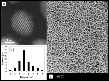
First, an optimized synthesis procedure for ITO nanoparticles is examined. The major requirement for ITO nanoparticles in electrode applications is that the produced particles be monodisperse and of small diameter (≈10 nm or less).Reference Choi, Nam, Park, Seo and Park28 Figure 1 depicts the results of one nanoparticle synthesis strategy that meets these requirements.Reference Mahajeri, Voigt, Klupp Taylor, Reindl and Peukert25, Reference Gilstrap, Capozzi, Carson, Gerhardt and Summers29 As seen in the figure, the nanoparticles have a narrow size distribution centered around 5 nm and are completely non-agglomerated. These two properties are of critical importance since agglomeration and the presence of large nanoparticles may impart non-uniformities in final electrode properties by either increasing solution turbidity, decreasing film density, or by interfering with deposition methods (e.g., clogging deposition nozzles).Reference Reindl, Mahajeri, Hanft and Peukert21 Moreover, nanoparticles of small diameter are required in order to ensure that the final sintering step can employ the lowest temperature possible to allow maximum compatibility with low thermal budget substrates. Decreasing the diameter of the nanoparticles makes densification thermodynamically more favorable due to the increased influence of surface area effects, as described in the Ostwald ripening process.Reference Perelaer, Smith, Mager, Soltman, Volkman, Subramanian, Korvink and Schubert7, Reference Kim, Lee, Kim and Ikegami30
Chemically synthesized non-agglomerated indium tin oxide (ITO) nanoparticles.Reference Gilstrap, Capozzi, Carson, Gerhardt and Summers29 (a) High-resolution scanning transmission electron microscopy (TEM) image of a 5 nm crystalline ITO nanoparticle. (b) Histogram of size distribution of 300 particles. (c) TEM image of highly uniform and non-agglomerated ITO nanoparticles. Reproduced with permission from Reference Reference Gilstrap, Capozzi, Carson, Gerhardt and Summers29. ©2008, Wiley-VCH Verlag GmbH & Co. KGaA.

Although a wide variety of solution-based deposition methods for ITO nanoparticles exist (e.g., doctor blading,Reference Maksimenko and Wellmann31 spin coating,Reference Ederth, Johnsson, Niklasson, Hoel, Hultaker, Heszler, Granqvist, van Doorn, Jongerius and Burgard26 dipping,Reference Puetz, Al-Dahoudi and Aegerter20, Reference Goebbert, Nonninger, Aegerter and Schmidt32 spraying,Reference Al-Dahoudi, Bisht, Göbbert, Krajewski and Aegerter22 screen printing,Reference Takeda, Kato, Higuchi, Takeichi, Motohiro, Fukumoto, Sano and Toyoda33 gravure printing,Reference Puetz and Aegerter34 and layer-by-layer assemblyReference Peng, Thio and Gerhardt35), the inkjet printing method has received much attention as a result of its unique advantages, as compared to other methods. Significantly, inkjet printing is capable of fast and precise direct writing combined with an efficient material usage, qualities that are highly desired in industrial applications. Specifically, print resolutions down to 20 μm and firing speeds of 100 kHz are feasible. Inkjet printing, however, is a complicated process where a few factors, such as ink chemistry and jetting nozzle design, greatly affect the behavior of ejected printed drops and their subsequent evaporation, which in turn affects deposited film quality.Reference Singh, Haverinen, Dhagat and Jabbour12 To address these issues, there have been several published reports detailing efforts to optimize the inkjet printing of ITO nanoparticles.Reference Sung-Jei, Yong-Hoon and Jeong-In17, Reference Jeong, Kim and Kim36
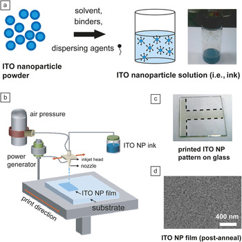
One recent study by Jeong et al. demonstrated the inkjet printing of transparent ITO nanoparticle-based electrodes on glass using a piezoelectric drop-on-demand inkjet printer.Reference Jeong and Kim37 The process flow for this deposition is shown in Figure 2. As the first step in such an inkjet printing process, synthesized nanoparticles are dispersed into solution to form a nanoparticle ink, as shown in Figure 2a. In addition to the necessary solvent (e.g., ethanol), dispersants and binders may also be added to the solution in this step. Next, inkjet printing of the ITO nanoparticle ink onto target substrates is performed, as illustrated in Figure 2b. Multiple successive drops onto the same area may be used to build up film thicknesses to the desired amount. Lastly, a post-deposition sinter (between 300°C and 500°C) is carried out to increase the conductivity of the deposited ITO film.
Inkjet printing of indium tin oxide (ITO) nanoparticles (NPs).Reference Jeong, Lee, Kim, Kim and Na2 (a) Process flow for formation of an ITO nanoparticle solution (i.e., ink). (b) Schematic of the ITO NP piezoelectric inkjet printing system. (c) Photo of an ITO NP electrode patterned onto glass by inkjet printing; the electrode pattern is indicated by hyphenated lines. (d) Scanning electron microscopy image of the ITO NP electrode after annealing at 450°C showing its interconnected, porous structure. Reprinted with permission from Reference Reference Jeong, Lee, Kim, Kim and Na2. ©2010, Elsevier.

The aforementioned study, utilizing ≈25 nm diameter ITO nanoparticles and a 450°C post-printing sinter, yielded optically transparent printed ITO nanoparticle electrodes on a glass substrate, as shown in Figure 2c. Scanning electron microscopy imaging of the ITO nanoparticle film (Figure 2d) revealed a porous morphology; however, a large number of interconnecting particle necks is evident, suggesting substantial conductivity. Electrical testing confirmed this; the printed ITO films possessed a resistivity value of 1.52 × 10⁻² Ω∙cm (sheet resistance of 202.7 Ω/sq, at ≈750 nm thickness), with a transparency value of ≈86%. Although this recent report is promising, future work to further reduce the temperature of the post-deposition sinter step is needed before the inkjet printing of ITO nanoparticles, especially on low thermal budget substrates, will become practical.
To address this substrate temperature restriction, a variety of strategies exist for obviating the need for a high-temperature nanoparticle sintering process. The most widely examined method utilizes UV-curable polymer binders in place of the typical thermally curable type.Reference Aegerter, Puetz, Gasparro and Al-Dahoudi38 One recent study by Heusing et al. employed two UV-curable polymer binders, polyvinylpyrrolidone (PVP) and 3-methacryloxypropyltrimethoxysilane, in combination with low-temperature annealing (130°C), to achieve spin-cast ITO nanoparticle films on glass and poly(ethylene terephthalate) (PET) substrates, with resistivities as low as 1.0 × 10⁻¹ Ω∙cm, a sheet resistance of 750 Ω/sq, and a transparency of ≈86%.Reference Heusing, de Oliveira, Kraker, Haase, Palfinger and Veith39 Such ITO film resistivities, although still much larger than those of sputtered ITO thin films, were obtained using a low-temperature, solution-based process, upon further improvement may represent a practical, low-cost method for ITO film deposition on flexible substrates.Reference Ederth, Johnsson, Niklasson, Hoel, Hultaker, Heszler, Granqvist, van Doorn, Jongerius and Burgard26
An alternative densification technique, termed the compression method, utilizes perpendicularly applied pressures (on the order of 100 MPa) to compress the as-deposited, porous nanoparticle films. Physical compression of a nanoparticle film acts to increase its density and consequently its conductivity.Reference Lindström, Holmberg, Magnusson, Lindquist, Malmqvist and Hagfeldt40, Reference Bühler, Thölmann and Feldmann41 Interestingly enough, although large applied pressures are required, the compression method has been shown to be compatible with flexible substrates, such as PET plastic films, for the fabrication of flexible nanoparticle-based electrodes.Reference Halme, Saarinen and Lund42 Lastly, laser annealing (i.e., treatment) of ITO nanoparticle films has also been shown to be a possible method to achieve film densification;Reference Königer, Rechtenwald, Al-Naimi, Frick, Schmidt and Münstedt14 however, due to the serial nature of the beam scanning process, laser annealing may not provide enough throughput for large-scale ITO depositions.
ITO nanowires
ITO nanowires are high-aspect ratio, one-dimensional materials that possess several important advantages as compared to both ITO nanoparticles and conventional polycrystalline ITO thin films. ITO nanowires can be grown with uniform morphologies consisting of narrow widths (≈10 nm to 100 nm), long axial lengths (up to hundreds of micrometers), smooth interfaces, and a highly crystalline atomic structure. Such a combination of features makes ITO nanowires a very attractive transparent electrode material. In particular, the long and continuous morphology of ITO nanowires provides an uninterrupted conduction pathway that greatly increases conductivity by reducing grain boundary scattering and indirect conduction paths that are present in discontinuous ITO nanoparticle films.Reference Halme, Saarinen and Lund42–Reference Greer and Street44
ITO nanowires have been grown using a variety of methods, with the most extensively explored route being vapor phase growth, and the lesser being solution-based synthesis. The most widely reported vapor phase growth methods include pulsed laser deposition,Reference Savu and Joanni45 molecular beam epitaxy (MBE),Reference O’Dwyer, Szachowicz, Visimberga, Lavayen, Newcomb and Torres3 and vapor transport growth,Reference Wan, Dattoli, Fung, Guo, Chen, Pan and Lu46 which all typically require temperatures exceeding 500°C. The common feature among all these methods is that the ITO nanowires are grown in a catalyzed process termed vapor-liquid-solid (VLS) growth.Reference Lu and Lieber47 In the VLS process, a metal nanoparticle (e.g., Au or In) characteristically serves as the nanowire nucleation site and catalyzes subsequent nanowire longitudinal growth. The size of the catalyst nanoparticle directly determines the diameter of grown nanowires; thus nanowires of an appropriate diameter may be grown to satisfy application-specific requirements.
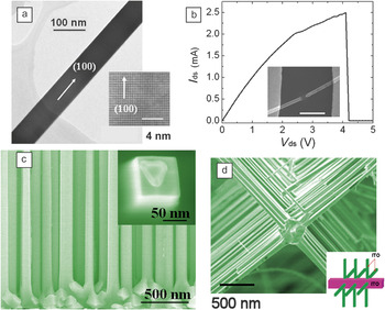
In contrast, solution-based growth methods such as electrospinning,Reference Munir, Iskandar, Yun, Okuyama and Abdullah48 sol-gel,Reference Wang, Ting, Hung, Chiou, Liu, Liu, Ratinac and Ringer49 and electrophoreticReference Kovtyukhova and Mallouk50 deposition typically require lower growth temperatures, but have mostly been limited to producing nano- or polycrystalline ITO nanowires. As a result, solution-grown ITO nanowires typically possess a higher resistivity (≈100 Ω∙cm) as compared to vapor phase grown, single-crystal ITO nanowires (≈10–4 Ω∙cm).Reference Kovtyukhova and Mallouk50 Due to their relatively low conductivity levels, solution-grown ITO nanowires presently are unsuitable for use in transparent electrodes, although further improvements in such growth methods may provide a viable low-cost option for ITO nanowire synthesis in the future. As a result of this limitation, the rest of this discussion will present an overview of recent efforts to evaluate the performance of non-solution grown ITO nanowires that are presently better suited for use in transparent electrodes. Note that the studies to be discussed here report on the fundamental properties of non-solution grown ITO nanowires; they do not examine the potential compatibility of ITO nanowires with practical solution processing/deposition techniques. In a study by Wan et al.,Reference O’Dwyer, Szachowicz, Visimberga, Lavayen, Newcomb and Torres3 individual ITO nanowires grown by a vapor transport method were shown to be high-performance transparent conductors, with resistivity values (lowest measured wire resistivity of 6.29 × 10⁻⁵ Ω∙cm) and transparency values (≈85% for a spin-cast ≈500 nm thick nanowire film) comparable to the best quantities achieved in high-quality deposited ITO thin films. Transmission electron microscopy studies (Figure 3a) verified that the ITO nanowires were low-defect, single-crystalline materials with a uniform diameter and smooth exterior interfaces. As a result of their high-quality material structure, current-voltage (I-V) measurements on individual ITO nanowires revealed that they could withstand large current densities. The ITO nanowire shown in Figure 3b endured a current density of 3.1 × 10⁷ A/cm2 before failure by Joule heating induced melting; such a large current density is comparable to other highly conductive single-crystal nanowires (e.g., NiSi).Reference Wu, Xiang, Yang, Lu and Lieber51
Indium tin oxide (ITO) nanowires.Reference Wan, Dattoli, Fung, Guo, Chen, Pan and Lu46, Reference Wan, Wei, Zhi, MacManus-Driscoll and Blamire54 (a) Transmission electron microscopy and high-resolution transmission electron microscopy (inset) of an ITO nanowire. (b) I-V measurement of an ITO nanowire with a resistivity of 2.66 × 10⁻⁴ Ω∙cm. The nanowire can carry a current of more than 2.5 mA before breaking down. Inset, scanning electron microscopy (SEM) image of the failed ITO nanowire. Scale bar: 500 nm. (c) Side-view SEM image of an ITO nanowire array showing the epitaxial, vertical growth of the nanowires from the ITO/yttria-stabilized zirconia substrate. Inset, top-view SEM image of a single ITO nanowire. Adapted with permission from Reference Reference Wan, Dattoli, Fung, Guo, Chen, Pan and Lu46. ©2006, American Chemical Society. (d) SEM image of a branched ITO nanowire. Inset, diagram of the three-dimensional branched nanowire structure. Reproduced with permission from Reference Reference Wan, Wei, Zhi, MacManus-Driscoll and Blamire54. ©Wiley-VCH Verlag GmbH & Co. KGaA.

Studies have also demonstrated the growth of vertical ITO nanowire arrays through proper epitaxial matching of the ITO nanowire latticeReference Gao, Chen, Li, Jiang, Ye, Ma, Chen, Xiong, Sun and Wu52 to an underlying single-crystal ITO thin film (Figure 3c). Such a configuration, consisting of arrays of vertically oriented nanowires anchored by an underlying TCO thin film, has been hypothesized to serve as a highly efficient charge collection electrode in both dye-sensitized and polymer solar cells.Reference Wang, Ting, Hung, Chiou, Liu, Liu, Ratinac and Ringer49, Reference Hochbaum and Yang53 In particular, the highly packed and uniform vertical ITO nanowire array can provide a direct and low-resistance conduction pathway to the underlying thin-film electrode as compared to the indirect, percolating charge transport present in conventionally used, nanoparticle-based charge collection electrodes.
The flexibility of the nanowire approach was further demonstrated by branched, three-dimensional ITO nanowire arrays in an additional study.Reference Wan, Wei, Zhi, MacManus-Driscoll and Blamire54 Utilizing a second VLS growth step on already-grown ITO nanowire “backbones,” epitaxial ITO nanowire branches were synthesized (Figure 3d). As a result of the epitaxial relationship between the 3D rectangular-shaped ITO nanowire backbone and its branches, a fourfold symmetry among the branch growth directions was realized. Moreover, due to this epitaxial relationship, branches were found to be highly aligned in the same parallel direction on each face of the ITO nanowire backbone. Importantly, the large surface area provided by this branched and interconnected ITO nanowire structure could serve as a highly efficient charge collection electrode (e.g., in solar cell applications).
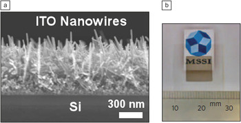
As opposed to such highly controlled nanowire morphologies, grown layers of freestanding albeit randomly oriented nanowires (i.e., “nanowire forests”) may provide an adequate level of performance for some electrode applications.Reference Gao, Chen, Li, Jiang, Ye, Ma, Chen, Xiong, Sun and Wu52 For instance, in a study by O’Dwyer et al., ITO nanowires were grown directly on the top surface of a heavily p-doped Si capping layer on a Si/SiGe multiple quantum well LED device. The MBE-grown ITO nanowire layer consisted of randomly oriented ITO nanowires, which served as the transparent electrode in the top-emission LED (Figure 4a).Reference O’Dwyer, Szachowicz, Visimberga, Lavayen, Newcomb and Torres3 The nanowire-based electrode, as a result of its superior anti-reflection properties, was found to outperform both traditionally used semi-transparent NiCr thin films and ITO thin films as the transparent electrode material in the LED device.Reference O’Dwyer, Szachowicz, Visimberga, Lavayen, Newcomb and Torres3
Indium tin oxide (ITO) nanowires as a transparent electrode.Reference O’Dwyer, Szachowicz, Visimberga, Lavayen, Newcomb and Torres3 (a) Cross-sectional scanning electron microscopy image of an ITO nanowire layer contacting a silicon-based light-emitting diode. As a consequence of the chosen molecular beam epitaxy growth procedure, many of the ITO nanowires are branched. (b) Photo of an ITO nanowire layer deposited under similar conditions on a glass cover slip. The layer is highly transparent and anti-reflecting. Reprinted with permission from Reference Reference O’Dwyer, Szachowicz, Visimberga, Lavayen, Newcomb and Torres3. ©2009, Macmillan Publishers Ltd.

The source of the ITO nanowire layer’s higher performance, its anti-reflection properties, could be attributed to the porosity of the nanowire forest morphology. This porosity caused the nanowire layer to effectively behave as a graded refractive index medium, which served to gradually reduce the refractive index of the LED’s silicon layer to the index of the surrounding air medium.Reference Kim, Chhajed, Schubert, Schubert, Fischer, Crawford, Cho, Kim and Sone55 The resultant anti-reflection property produced a substantial reduction in Fresnel reflection at the air/ITO nanowire layer interface. For instance, the reflectivity of an ITO nanowire/silicon substrate was reduced to 6% from a value of 55% for a standard ITO thin-film coating on silicon (λ = 600 nm). As shown in Figure 4b, the anti-reflection property of the ITO nanowire film is evidenced by the glare-free and dark surface of the film. Electrical measurements on the as-grown ITO nanowire layers revealed film resistivity levels in the range of 1 × 10⁻⁴ Ω∙cm to 4 × 10⁻⁴ Ω∙cm, consistent with previously described studies on individual ITO nanowires.Reference O’Dwyer, Szachowicz, Visimberga, Lavayen, Newcomb and Torres3 Prospectively, electrodes made out of such highly non-reflecting ITO nanowire layers may be utilized in the future to increase the light transmission efficiency in a variety of optoelectronic devices, such as LEDs or solar cells.Reference Gevaux56
Although these early reports on ITO nanowires are promising, little research has been conducted on the solution-based deposition of ITO nanowire films. However, nanowire solution-deposition is entirely feasible; studies have demonstrated the fluidic-flow,Reference Huang, Duan, Wei and Lieber57 dielectrophoretic,Reference Smith, Nordquist, Jackson, Mayer, Martin, Mbindyo and Mallouk58 layer-by-layer,Reference Shim, Podsiadlo, Lilly, Agarwal, Lee, Tang, Ho, Ingle, Paterson, Lu and Kotov59 inkjet printing,Reference Noh, Cheng, Sirringhaus, Sohn, Welland and Kang60 and Langmuir-BlodgettReference Whang, Jin, Wu and Lieber61 deposition of nanowires based on non-ITO constituent materials, such as silicon. These methods, although still under development, should be applicable to the solution deposition of ITO nanowires that one day may enable higher performance (i.e., higher conductivity) solution-deposited ITO electrodes.
Summary and outlook
ITO is a material of immense economic importance; notably, the 2009 market revenue for ITO electrodes exceeded $3 billion. By 2016, one prediction has that amount growing to an excess of $10 billion; with the maturing segment of rigid flat panel displays accounting for the majority of the growth.Reference Baraton1 Although these numbers may be impressive, the story is not over yet for ITO, as the rapidly growing area of printed electronics represents another market where ITO’s unique combination of high transparency and conductivity may be of prime importance. The field of printed electronics, which includes a variety of devices such as displays and solar cells, is primed for rapid growth, with some projections of over $300 billion in revenue by 2030.Reference Singh, Haverinen, Dhagat and Jabbour12, Reference Takeda, Kato, Higuchi, Takeichi, Motohiro, Fukumoto, Sano and Toyoda33 In order for ITO to play a role in this expanding market, the development of practical methods for the solution-deposition of ITO in the form of solution-dispersible ITO nanowires and nanoparticles is necessary.
Presently, the solution-deposition of ITO nanowires and nanoparticles to realize transparent and flexible ITO electrodes has been demonstrated but is of limited practical use due to still suboptimal performance levels. In particular, the resistance levels of such electrodes (sheet resistances of ≈200 Ω/sq) are much higher as compared to those of PVD-deposited ITO films (sheet resistances of ≈10 Ω/sq) for relatively similar transparency levels (>80%). To rectify this issue, further improvement of the synthesis, dispersion, and deposition procedures for ITO nanowires and ITO nanoparticles is still required. A great deal of progress in this field, however, has already been achieved in a short amount of time, leaving one optimistic that the future remains bright for ITO nanowire- and nanoparticle-based transparent and flexible films.
Acknowledgments
This work was supported, in part, by the National Science Foundation (ECCS-0804863). E.N.D. acknowledges support provided through the NIST-National Research Council (NRC) Postdoctoral Associateship Program.