Introduction
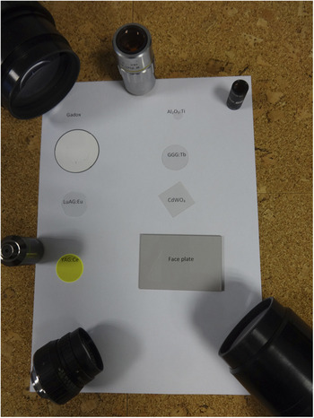
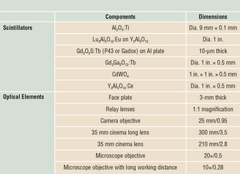
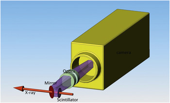
Ionizing radiation-to-visible-light converters, called scintillators, are essential in x-ray imaging, x-ray beam monitoring, and x-ray counter applications, and are deployed for hard x-ray energy applications. The main advantages of indirect detectors, which consist of a scintillator and a photon detector, are that they cover a range of pixel sizes, from 100 nm to millimeter size, they can be used for time-resolved experiments, and they are radiation hard (resistant). An additional advantage is that they represent an efficient way to detect x-rays up to 100 keV or more in energy and can handle very high fluxes. Figure 1 shows examples of scintillators and their optical coupling; Table I lists these components and their dimensions. For additional information, please see Table SI, available online. The use of high x-ray energy or high flux requires specific optomechanical engineering design. One example is to remove the optics from the direct x-ray path as shown in Figure 2 . Reference Tucoulou, Martinez-Criado, Bleuet, Kieffer, Cloetens, Labouré, Martin, Guilloud and Sussini1
Examples of scintillators and their optical elements for x-ray imaging and beam monitoring in synchrotron radiation.

Composition and dimensions of scintillators and optical elements in Figure 1.

Optical scheme of an indirect detector for x-ray imaging or beam monitoring applications under strong radiation. Reference Tucoulou, Martinez-Criado, Bleuet, Kieffer, Cloetens, Labouré, Martin, Guilloud and Sussini1 Photo courtesy of J. Borrel, European Synchrotron Radiation Facility.

Characteristics of the scintillating material
The desired characteristics of scintillators are strongly dependent on the application for which they are used. In the case of x-ray imaging, the required characteristics include the following:
-
• X-ray absorption: Maximize the x-ray stopping power by the couple ρ.Z eff, where ρ and Z eff are the density and effective atomic number of the scintillator, respectively.
-
• Light emission: High conversion efficiency (>15 photons/keV), where the emission wavelength of the scintillator must match the spectral sensitivity of the imaging sensor and the flux must match the dynamic range.
-
• Timing: Time-resolved experiments require fast decay time (<100 ns); low light remanence, so-called afterglow, (4–5 decades @ ms scale) is mandatory for precision measurements.
-
• Low gain hysteresis: The variation of light output resulting from radiation damage must be minimized.
-
• Optical properties: High transmittance of the scintillator, radiation hardness, and no optical scattering for high spatial resolution.
-
• Technical aspects: Machinable, nontoxic, and good mechanical strength.
Scintillators for x-ray beam viewers must satisfy two requirements. The first concerns permanent x-ray transmissive scintillators for real-time x-ray beam monitoring applications. This means that the x-ray beam must remain available to perform experiments with samples. The scintillator itself then becomes an optical element in the x-ray path and therefore must avoid aberration in the transmitted beam (e.g., x-ray fluorescence). The scintillator must provide a significant signal to the imaging sensor, but absorbs less than 10% of the x-ray beam so that sufficient x-rays are transmitted to the sample for the experiment (this is also referred to as noninvasive). The second requirement concerns systems that intercept the x-ray beam. In this case, most of the x-ray beam must be fully or partially absorbed by the scintillator (invasive). Both systems can operate in air or ultrahigh vacuum (UHV) conditions.
At the physical sensor level, the bandwidth of the beam (i.e., white, pink—produced by using an x-ray mirror and filters—and monochromatic beam monitoring) qualitatively presents different technical problems. Pink and white beams exhibit a higher intensity than monochromatic and, consequently, a heat load develops due to x-ray absorption. The required characteristics of invasive and noninvasive beam viewers are:
-
• X-ray absorption: The stopping power is expected to be below 10% for the transmissive version. Two strategies for achieving this are possible: (1) thin, high-Z, high-density material (e.g., Lu2O3); and (2) thicker, low-Z, low-density material (e.g., sapphire:Ti, ruby, diamond, boron nitride [BN]).
-
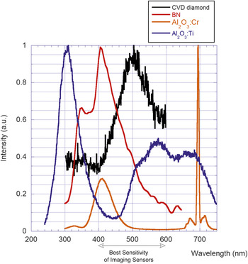
• The light emission, optical properties, and technical aspects are similar to the scintillator for x-ray imaging. The spectra of noninvasive screens are plotted in Figure 3 . Reference Martin, Baret, Lesimple and Jobert2
X-ray excited spectra of several screens for a noninvasive beam viewer. Reference Martin, Baret, Lesimple and Jobert2

Scintillators are also used as x-ray counters and form the basis of efficient detectors for high x-ray energy owing to their characteristics—strong stopping power, good timing characteristics, high light output, and excellent technological maturity.
Scintillating screens for x-ray imaging
As discussed in the Introduction section, the x-ray stopping power is the most critical parameter for scintillators. Inorganic scintillators with a thickness range from 1 µm to 500 µm are deployed in most imaging applications requiring an x-ray-to-light converter. In two-dimensional detectors, powder phosphor screens, thin single-crystal (SC) plates, and single-crystal films (SCFs)—films with thicknesses below 20 μm—are used the most on beamlines. Nevertheless, scintillators grown in columnar structures and ceramic materials are becoming competitive in terms of spatial resolution-absorption and optical quality, respectively. These scintillators for x-ray imaging applications are described and listed in Table SI.
Powder screens
In powder screens, small “phosphor” grains (typically 1–10 µm size) are mixed with a binding agent and are processed to a film. A qualitative list of powder screens is described by Shionoya and Yen in a phosphor handbook. Reference Shionoya and Yen3 The main powder screens used for x-ray detection at synchrotrons are made of Gd2O2S:Tb (P43 or Gadox) and Y3Al5O12:Ce (P46). Due to the granulometry and morphology of powders, their density is approximately one-half of the pure material. Phosphor screens are not optimized for spatial resolution due to the scattered light emission; the spatial resolution is approximately proportional to screen thickness. They are typically inexpensive and easily deposited on polymer, aluminum, aluminized mylar, glass, and tapered fiber optics. Phosphor screens can be also deposited onto an imaging sensor surface, such as charge-coupled devices, to improve the contrast transfer function. Reference Gambacini, Taibi, Del Guerra, Marziani and Tuffanelli4
Single-crystal scintillators
Single-crystal scintillators offer better stopping power and spatial resolution than phosphor screens, however, they are more expensive. They are mechanically stable and are used in thicknesses down to 25 µm as freestanding sensors. A thinner crystal is possible, down to 5 µm, but it will need to be mounted on a frame such as a glass substrate or a ceramic ring. The most common SCs on synchrotron sources for x-ray imaging applications are the garnets yttrium-aluminim-garnet:Ce (Y3Al5O12:Ce, namely YAG:Ce) and lutetium-aluminum-garnet:Ce(Lu3Al5O12:Ce, namely LuAG:Ce). Reference Lecoq, Getkin and Korzhik5
Other scintillators such as lutetium-orthosilicate:Ce(LSO:Ce) and lutetium-yttrium orthosilicate:Ce((Lu,Y)2SiO5:Ce namely LYSO:Ce), which have a higher stopping power, are also used. Their main advantages are their fast decay time (∼40 ns) and good light yield (∼30 ph/keV). Reference Lecoq, Getkin and Korzhik5 Their emission length at 420 nm could be an obstacle for their integration in some optics that have a bad transmission in the blue region.
While cadmium tungstate (ρ = 7.9 g/cm3, Z eff = 66, light yield [LY] = 12 ph/keV) and lead tungstate (ρ = 8.3 g/cm3, Z eff = 73, LY = 0.2 ph/keV), materials are dense and quite attractive, only the CdWO4 can be used owing to the required minimum of light yield. The high refractive index of tungstate scintillating material (n ∼ 2.2) reduces the collection efficiency of the optical system.
Structured and semistructured scintillators
CsI(Tl) and ZnSe can be grown in a microcolumnar shape by chemical vapor deposition. Reference Thacker, Yang, Packard, Gaysinskiy, Burkett, Miller, Boone and Nagarkar6 The semistructured form, which is based on a columnar shape with a grain boundary as interface, guides visible light to the imaging sensor. The needle diameter varies from 1 to 30 µm, and the thickness can be up to 2–3 mm. Light crosstalk between needles is present, but limited, and better spatial resolution is obtained compared to an unstructured powder screen. Thallium-doped CsI is the most deployed semistructured scintillator owing to its excellent morphology and scintillation properties.
When the thickness of semistructured scintillators is increased, the spatial resolution drops significantly because the spreading of the light increases with the thickness of the scintillator. Scintillating fiber-optic (SFO) plates are an alternative solution. They allow the increase in stopping power, while maintaining the spatial resolution, owing to the difference in the refractive indices between the core (luminescent glass known as LKH-6, n = 1.58) and the cladding (n = 1.48). Reference Gennaro, Malvestio, Zanella and Zannoni7 In addition, the presence of an extramural absorber between fibers improves the spatial resolution by reducing the crosstalk between fibers. The LKH-6 SFO is a terbium-doped glass, Reference Gennaro, Malvestio, Zanella and Zannoni7 which can be produced with diameters ranging from a few µm to millimeters and with thickness up to 2–3 cm. If radiation hardness is an asset of the LKH-6 SFO, its strong afterglow limits its application at low dynamic range.
When contrast and dynamic range are both required, the structured scintillator, which consists of an array of deep pores in silicon filled with CsI(Tl), is more appropriate. Reference Sahlholm, Svenonius, Näsgarde, Wiklund and Linnros8 This technology has been developed by ScintX and its advantage is that the silicon pores guide the light to the imaging sensor with no crosstalk. The technology has only been applied to CsI(Tl) scintillators owing to its low melting point (621°C), which is useful to fill the pores as compared to garnet (melting point: 1980°C) and orthosilicate (2050°C) scintillating materials.
Single-crystal films
Submicrometric spatial resolution requires 1–20-µm-thin scintillators. In this case, the scintillator must exhibit excellent optical quality and be mechanically stable to ensure perfect focalization of the optical system into the sensitive depths of the scintillator. Reference Koch, Raven, Spanne and Snigirev9
Ce-doped yttrium, and europium- and terbium-doped lutetium aluminum garnets in the form of SCFs have been grown by liquid-phase epitaxy (LPE) on an undoped YAG substrate. The optical quality and radiation hardness of these garnet materials are excellent, and LuAG offers a good stopping power. The main issue with these scintillating devices is the luminescence of the YAG substrate under x-ray irradiation. The substrate produces light, which degrades the spatial resolution. Reference Koch, Cloetens, Ludwig, Labiche and Ferrand10
Europium- and terbium-doped gadolinium gallium garnets (GGGs) have been grown on undoped GGGs. The stopping power of GGG is rather high and comparable to that of LuAG; the gadolinium K-edge improves the absorption efficiency above 51 keV. The scintillation performance of GGGs is excellent in terms of light yield and afterglow. Reference Martin, Couchaud, Ferrand, Caillet, Pelenc, Chambaz, Passero, Getkin and Grinyov11 An excellent spatial resolution down to 300 nm and 9.8 µs temporal resolution was demonstrated by Jung using GGG:Tb. Reference Jung, Lee, Kwon, Park, Chang, Kim, Pyo, Kohmura, Nishino, Yamamoto, Ishikawa and Je12
Ce-doped lutetium orthosilicate is well deployed for positron emission tomography applications in the SC structure owing to its fast decay time and good absorption. Reference Melcher, Eriksson, Aykac, Bauer, Williams, Loope, Schmand, Tavernier, Gektin, Grinyov and Moses13 Cerium emission at 400 nm is not well matched with the quantum efficiency of imaging sensors and also not adapted for the optics, which exhibit a poor transmission in UV and blue band. Reference Martin, Douissard, Seeley, Cherepy, Payne, Mathieu and Schulanden14 Douissard Reference Douissard, Cecilia, Martin, Chevalier, Couchaud, Baumbach, Dupré, Kühbacher and Rack15 proposed terbium-doped LSO SCF, which is slower, but exhibits a peak emission at 550 nm and is therefore more suitable for imaging applications. LSO:Tb is an excellent scintillator when high spatial resolution is required. In addition, time-resolved images have been demonstrated with excellent spatial and temporal resolution of 500 nm and 8 ms, respectively. Reference Soeun, Namseop, Jinkyung, Yoshiki, Tetsuya, Kook, Ho and Akira16
Ceramics
Ceramic plates are becoming an alternative to SC scintillators and are increasingly interesting for x-ray imaging applications owing to their low manufacturing cost Reference Cherepy, Kuntz, Roberts, Hurst, Drury, Sanner, Tillotson and Payne17 and potentially large size. Their development started through the demands of laser applications in the 1990s; today, thin ceramic YAG:Ce scintillators, bounded by solid-state diffusion on undoped YAG substrate, are used at the Spring8 synchroton in Japan. 18 Kameshima Reference Kameshima, Sato, Kudo, Ono, Ozaki, Katayama, Hatsui and Yabashi19 demonstrated x-ray imaging capability with a YAG:Ce scintillator, in a thickness range from 5 µm to 1.5 mm, and has reached 8-µm spatial resolution. This is also used as a sensor to monitor the x-ray free-electron laser (XFEL) beam and for wavefront measurement.
Scintillating screens for x-ray beam diagnostics
A well-established method to visualize the x-ray beam profile and position is to use a converter screen such as a phosphor, a scintillator, or a polycrystalline chemical-vapor-deposited (CVD) diamond screen. Other parameters may also be derived from such measurements (e.g., beam intensity or the spectral distribution after a grating). The visible image from the scintillator is relayed by lens optics to a camera analysis system. The most critical component is the scintillator, since it has to withstand high beam intensities and short pulses. The scintillator has to provide high dynamic range and fast time response, often in a UHV environment. The screen may fully or partially absorb the x-ray beam. In the latter case, an obvious solution is to replace the in-beam phosphor screen (e.g., YAG:Ce) Reference Bordessoule20 by a thin film (e.g., 500-nm Lu2O3) Reference Pereira, Martin, Levinta and Dujardin21 or a low-Z converter screen (e.g., CVD diamond, Reference Degenhardt, Aprigliano, Schulte-Schrepping, Hahn, Grabosh and Wörner22 sapphire:Ti, Reference Tucoulou, Martinez-Criado, Bleuet, Kieffer, Cloetens, Labouré, Martin, Guilloud and Sussini1 ruby, Reference Hosono, Nihei and Nakazama23 or BN24).
X-ray pulses from XFELs can be short (10 fs) and intense (10 mJ/mm2) with high repetition rates (MHz). These pulse intensities may alter or destroy the target material. A good criterion of the single-shot damage threshold is the number of pulses required to reach the melting point: Reference Koch, Freund, Grünert, Planas, Roth, Samoylova, Lyamayev and Biedron24,Reference Hau-Riege, London, Bionta, McKernan, Baker, Krzywinski, Sobierajski, Nietubyc, Pelka, Jurek, Juha, Chalupský, Cihelka, Hájková, Velyhan, Krása, Kuba, Tiedtke, Toleikis, Tschentscher, Wabnitz, Bergh, Caleman, Sokolowski-Tinten, Stojanovic and Zastrau25
 $${N_{\max }}\, = \,\Delta {T_{\max }}\,2\pi \,{\sigma ^2}\,{l_{{\rm{abs}}}}\,\rho \,{c_{\rm{p}}}\,/\,{Q_0},$$
where ΔT max is the increase from ambient to melting temperature, σ = fwhm/2.35 the beam diameter (full width of the beam profile at half maximum amplitude divided by 2.35× the x-ray beam diameter), l abs is the x-ray absorption length in the scintillator, ρ its density, c p the specific heat, and Q 0 the pulse energy. Heat transfer is not considered in this formula.
As a result of their low atomic number and high melting point, diamond and BN are more resistant than YAG:Ce by one order of magnitude for photon energies of 3 keV. Diamond as a polycrystalline CVD material has a complex photoluminescence spectrum; the light yield is considerably increased by doping with nitrogen or boron. Reference Manfredotti, Vittone, Lo Giudice, Paolini, Fizzotti, Dinca, Ralchenko and Nistor26,Reference Iakoubovskii and Adriaenssens27
Pyrolytic hexagonal boron nitride is a ceramic material that is easily machined to large and thin layers at moderate cost. The CVD process allows a more pure material with well-defined luminescence properties in the blue/ultraviolet (UV) band. Reference Museur and Kanaev28 Measured decay constants of 30 ns for this material are faster than for YAG:Ce and may allow single pulse detection in certain operating modes at synchrotrons or free-electron lasers. Reference Museur and Kanaev29
For beam diagnostic applications that require high light yield, combined with relatively high temporal resolution and UHV compatibility, Gd2O2S:Pr is interesting. It is manufactured for medical computed tomography with a decay constant of 2.5 µs and low afterglow. Reference van Eijk30 The material is a translucent ceramic. By its light-scattering property, it increases the light collection toward the optical system compared with transparent scintillating screens. This is a result of the Lambertian light-emitting characteristics of scattering screens. However, the light scattering within the screen reduces the spatial resolution.
Scintillator-based counters
Fast scintillator materials that can convert incoming high-energy photons into UV/visible photons within 10–100 ns or less can be used in scintillation detectors employed in photon (x- or γ-ray) counting. SCs of NaI:Tl were employed for this purpose in the late 1940s, Reference Hofstadter31 followed by a number of other SC materials. Reference Weber32,Reference Nikl and Yoshikawa33 The last two decades have focused on the study of Ce3+-doped and Pr3+-doped materials. Due to the allowed 5d–4f transition of Ce3+ or Pr3+ luminescent centers, the dominant decay component of scintillation response occurs with decay time values of 20–80 ns (Ce3+) or 10–25 ns (Pr3+). Most of these materials are also resistant against thermal quenching up to high temperatures of around 600–700 K. Reference Nikl and Yoshikawa33,Reference Bachmann, Ronda and Meijerink34
Among oxides, YAG:Ce has already been mentioned, and its scintillation characteristics were systematically reported in the 1990s. Reference Moszynski, Ludziejewski, Wolski, Klamra and Norlin35 Its high density analog, namely Lu3Al5O12:Ce (LuAG:Ce), became of interest after 2000 and further development resulted in the discovery of the multicomponent garnet SC family (Gd, Lu, Y)3(Al, Ga)5O12:Ce in 2011. Reference Nikl, Yoshikawa, Kamada, Nejezchleb, Stanek, Mares and Blazek36 Recently, the positive influence of divalent ion co-doping in these materials was found, which further accelerates scintillation response and limits afterglow, Reference Nikl, Kamada, Babin, Pejchal, Pilarova, Mihokova, Beitlerova, Bartosiewicz, Kurosawa and Yoshikawa37,Reference Lucchini, Babin, Bohacek, Gundacker, Kamada, Nikl, Petrosyan, Yoshikawa and Auffray38 similar to that found in orthosilicates and explained in terms of stabilization of the Ce4+ center. Reference Blahuta, Bessière, Viana and Ouspenski39
As the most promising multicomponent garnet host composition, Gd3Ga3Al2O12 (GAGG) was commercialized and is now available as 3-in. dia. Czochralski-grown crystals. Reference Kamada, Shoji, Kochurikhin, Okumura, Yamamoto, Nagura, Yeom, Kurosawa, Yokota, Ohashi, Nikl and Yoshikawa40 Optimized Ce-doped multicomponent garnets in the form of LPE-grown films recently reported a light yield comparable to that of high-quality GAGG:Ce bulk crystals (light yield above 50,000 photons/MeV) and an afterglow better by three orders of magnitude. Reference Prusa, Kucera, Mares, Onderisinova, Hanus, Babin, Beitlerova and Nikl41,Reference Zorenko, Gorbenko, Zorenko, Sidletskiy, Fedorov, Bilski and Twardak42 Mg co-doping has been applied in these thin-film scintillators as well, resulting in further improvement of their timing characteristics. Reference Průša, Kučera, Babin, Brůža, Pánek, Beitlerová, Mareš, Hanuš, Lučeničová and Nikl43
Even faster luminescence decay of Ce3+ and Pr3+ was obtained in an aluminum perovskite host, YAlO3 (YAP), where the room-temperature decay time values are 18 ns and 8 ns, respectively. Reference Weber44,Reference Gumanskaya, Korzhik, Smirnova, Pavlenko and Fedorov45 Scintillator performance was reported in the early 1980s. Reference Takeda, Miyata, Muramatsu and Tomiki46,Reference Autrata, Schauer, Kvapil and Kvapil47 To increase the density and effective atomic number, intense effort was carried out in several laboratories around the globe in the 1990s to prepare LuAP:Ce SCs, but due to the extreme instability of the perovskite phase, such SCs were difficult to grow and a mixed (Lu,Y)AlO3 host was finally chosen for further development. Reference Nikl48 Although a few companies were able to grow these to industrial size, Reference Trummer, Auffray, Lecoq, Petrosyan and Sempere-Roldan49 given their high price and lower light yield compared to YAP:Ce, they did not find commercial applications. (Lu, Gd)AlO3 host material was investigated in the form of LPE-grown SCF, however, the birefringence effect reduces optical performance. Reference Riva, Douissard, Martin, Carlà, Zorenko and Dujardin50
Among modern, fast halide scintillators, the rare-earth halides LaCl3:Ce and LaBr3:Ce must be mentioned. Reference Kramer, Dorenbos, Gudel and van Eijk51 LaBr3:Ce shows extremely high light yield and excellent energy resolution. On the other hand, these SCs are hygroscopic and show nonnegligible intrinsic radioactivity due to the presence of the isotope 138La, which has a natural abundance of 0.09% and half-life of 1011 years. Moreover, due to their high cost, applications are limited.
Perspectives
X-ray imaging synchronized on packets of electrons circulating in the storage ring (bunch structure) is a new technique that requires fast scintillators and strong radiation hardness. Rutherford Reference Rutherford, Chapman, White, Drakopoulos, Rack and Eakins52 performed an evaluation of scintillators. Due to high radiation stability, Ce-doped garnet scintillators are good candidates for ultrafast imaging. Nevertheless, these scintillators suffer from afterglow. The newly developed LuI3:Ce scintillator is an excellent candidate; Reference Marton, Miller, Ovechkina, Kenesei, Moore, Woods, Almer, Miceli, Singh and Nagarkar53 it is denser and faster (20 ns decay time) than garnet, and does not exhibit afterglow. While it is an attractive scintillator, it is a hygroscopic material and it is not commercially available today. Reference Marton, Nagarkar, Miller, Brecher, Bhandari, Kenesei, Ross, Almer and Singh54
As it exhibits a high stopping power, the Lu2O3 scintillator is considered an attractive material for x-ray imaging. It accepts many activators and is an excellent host matrix for different optics coupled to imaging sensors. In recent years, it has been developed in different crystalline forms, and now is available in SCF. Reference Riva, Martin, Douissard and Dujardin55 This last development allows good optical quality and x-ray imaging properties. Some progress is still needed in the field of large dimensions and better light yield for SC and SCF, respectively.
For short x-ray pulses at high pulse intensity requiring fast timing, h-BN deserves further investigation for beam-diagnostics applications. Fast exciton emission of multiple quantum wells based on GaN-GaInN nanostructures might also be interesting in this respect. Reference Hospodková, Nikl, Pacherová, Oswald, Brůža, Pánek, Foltynski, Hulicius, Beitlerová and Heuken56
Acknowledgment
Partial support of the Czech Science Foundation, Project No. 16-15569S, is gratefully acknowledged.

Thierry Martin is head of the Detector Unit at the European Synchrotron Radiation Facility (ESRF), France. He received his engineering degree from École Nationale Supérieure d’Ingénieurs de Caen, France, and his MSc degree in instrumentation at the University of Caen, France. He received his PhD degree from the University of Caen in 1998. He was a physicist at Smiths-Heimann, Germany, before joining ESRF as an engineer in 2000, focusing on high-spatial resolution detectors mostly based on scintillators, optics, imaging sensors, and x-ray beam monitors. Martin can be reached by phone at +33 4 76 88 2052 or by email at tmartin@esrf.fr.

Andreas Koch is a senior scientist at the European XFEL GmbH, Germany. He obtained his PhD degree at the Technical University of Hamburg, Germany. He has worked in public and private R&D departments (ESRF, Thales, and Philips) on x-ray imaging for applications in medical, nondestructive testing, and security. His research focuses on the development and implementation of imaging-based beam diagnostics. Koch can be reached by phone at +49 (0) 40 8998-6443 or by email at andreas.koch@xfel.eu.

Martin Nikl is a senior scientist and head of the Department of Optical Materials in the Institute of Physics of The Czech Academy of Sciences (AS CR) and associate professor at Czech Technical University in Prague, Czech Republic. He graduated from Czech Technical University in 1981, and received his CSc degree from the Institute of Physics, AS CR, in 1986. His current research interests include luminescence and scintillation materials, energy transfer and storage phenomena in the scintillation mechanism, physics of defects, luminescence of excitons, nanoaggregates, and quantum dots. Nikl can be reached by phone at +420 220 318 445 or by email at nikl@fzu.cz.