I. INTRODUCTION
Investigation of spinel materials with higher transparency and conductivity is the recent field of research because of their use in optoelectronic devices such as flat panel displays and solar cells. Reference Ahmad, Amin, Maqbool, Muhammad, Murtaza, Ali and Noor1 The general formula of Cr based spinel materials family is ACr2X4, in which A = Mn, Fe, Co, Ni, Cu Zn, and Cd, which occupy the tetrahedral site having charge +2. The X site accommodates various elements of group VI (i.e., O, S, Se and Te). These compounds generally exist in the cubic spinel structure. Reference Semari, Khenata, Rabah, Bouhemadou, Omran, Reshak and Rached2 Several of these compounds Reference Dekkers, Rijnders and Blank3–Reference Bouhemadou, Zerarga, Almuhayya and Omran7 are wide band gap semiconductors. These wide band gap materials are transparent in the visible and infrared regions. This has motivated to search for new spinel materials in optoelectronic devices. The electronic structure methods with accurate potential propose new and improved transparent and conducting materials.
Spinel compounds have been the subject of many experimental Reference Dekkers, Rijnders and Blank3–Reference Wei, Chen and Tang6 and theoretical Reference Bouhemadou, Zerarga, Almuhayya and Omran7–Reference Samanta and Saini17 works in the past few years, focused on their electronic and optical properties. The ternary spinel compounds CdCr2X4 (X = S, Se) with Cr as a transition metal are members of a group of chalcogenide semiconductors. These are ferromagnetic materials with Curie temperatures of 84.9 and 129 K, respectively. The structural properties such as lattice constant and anion parameter as well as magnetic and electrical properties of these compounds were studied in detail by Landolt-Börnstein. Reference Hellwege18 They were extensively studied due to a number of peculiar and interesting properties like giant magnetoresistance, photo-ferromagnetic effect, red shift of the optical absorption edge, and giant Faraday rotation apart from the coexistence of their semiconducting and ferromagnetic properties. These materials can be doped in a defined manner to achieve various properties using, e.g., Ag, In, Ga, and Br dopants and thereby fulfilling the basic requirements of a semiconductor material for technical applications. 19 Recently, the epitaxial growth of CdCr2Se4 films on both GaAs and GaP substrates provided an unprecedented opportunity to tune and optimize a spin-dependent behavior in semiconductor device heterostructures. Reference Park, Hanbicki, Mattson and Jonker20 Nikiforov has also done some magnetic and optical study of these compounds. Reference Nikiforov21 Lee et al. have studied some optical properties such as index of refraction. Reference Lee, Coburn and Gluck22 In addition to these experimental studies, some theoretical calculations have been performed on these spinels. Shanthi et al. have calculated the ab initio band structure of CdCr2S4 and CdCr2Se4, for both the nonmagnetic and the ferromagnetic states. Reference Shanthi, Mahadevan and Sarma23 Their calculations predict CdCr2S4 to be a ferromagnetic insulator and CdCr2Se4 to have a ferromagnetic semimetallic ground state with very low density of states (DOS) at the Fermi energy and a nearly gapped structure. Wang et al. studied the electronic band structure of ferromagnetic Cd x Cu1−x Cr2S4 and Cd x Cr1−x Cr2Se4 with exchange correlation potential GGA (generalized gradient approximation) and found CdCr2S4 and CdCr2Se4 to be semiconducting. Reference Wang, Gupta, Chshiev and Butler24 Fennie et al. Reference Fennie and Rabe25 have studied the dielectric properties of the ferromagnetic spinel CdCr2S4 from first principles within the Coulomb corrected local spin density approximation (LSDA+U).
Though a number of calculations exist for the electronic structure of CdCr2X4 (X = S, Se), Reference Shanthi, Mahadevan and Sarma23–Reference Fennie and Rabe25 there have been no attempt to study the optical properties even though data exist. Reference Ohgushi, Okimoto, Ogasawara, Miyasaka and Tokura26 Further orbital-independent TB-mBJ Reference Tran and Blaha27,Reference Koller, Tran and Blaha28 scheme for electronic structure calculations has not been used although TB-mBJ scheme is more accurate to predict the energy bands as compared to GGA and LSDA. Reference Reshak, Kamaruddin and Auluck29,Reference Reshak, Kamaruddin, Kityk and Auluck30 We tried to fill this gap. In this work, we present the full-potential linearized augmented plane wave (FP-LAPW) Reference Madsen, Blaha, Schwarz, Sjostedt and Nordstrom31–Reference Schwarz, Blaha and Madsen33 study of electronic and optical properties of CdCr2X4 (X = S, Se) normal spinals using an alternative form of the Coulomb corrected spin polarized generalized gradient approximation (GGA+U) Reference Anisimov, Zaanen and Andersen34,Reference Anisimov, Solovyev, Korotin, Czyzyk and Sawatzky35 and TB-mBJ scheme. Reference Tran and Blaha27,Reference Koller, Tran and Blaha28 The spin–orbit coupling is also added in both methods. Our results of calculated energy gap and optical properties are compared with the existing calculations Reference Wang, Gupta, Chshiev and Butler24,Reference Fennie and Rabe25 as well as the experimental data by Ohgushi et al. Reference Ohgushi, Okimoto, Ogasawara, Miyasaka and Tokura26
II. COMPUTATIONAL DETAILS
CdCr2X4 (X = S, Se) crystallizes in a cubic spinel structure with the space group
 $Fd\bar 3m$
(#227). The Cd ions are situated at the Wyckoff positions, 8a (1/8, 1/8, 1/8) tetrahedral sites, whereas the Cr ions are situated at the 16d (1/2, 1/2, 1/2) octahedral sites and the X ions at 32e (u, u, u) for normal spinels. Our calculations were carried out with scalar relativistic form of the FPLAPW method
Reference Madsen, Blaha, Schwarz, Sjostedt and Nordstrom31–Reference Schwarz, Blaha and Madsen33
based on density functional theory (DFT)
Reference Hohenberg and Kohn36
as implemented in the WIEN2k package.
Reference Blaha, Schwarz, Madsen, Kvasnicka and Luitz37
For exchange-correlation potential, we used the PBE
Reference Perdew, Burke and Ernzerhof38
(Perdew–Burke–Ernzerhof) version of the GGA+U
Reference Anisimov, Zaanen and Andersen34,Reference Anisimov, Solovyev, Korotin, Czyzyk and Sawatzky35
and TB-mBJ schemes.
Reference Tran and Blaha27,Reference Koller, Tran and Blaha28
In the full potential methods, the unit cell is divided into nonoverlapping spheres centered at atomic sites (muffin-tin spheres) of radius R
MT and an interstitial region. The R
MT are taken to be 2.5, 2.45, and 2.11 (a.u.) for Cd, Cr, and S, respectively, in the case of CdCr2S4 and 2.5, 2.41, and 2.41 (a.u.) for Cd, Cr, and Se in the case of CdCr2Se4. The plane wave expansion of the wave function in the interstitial region was truncated at R
MT
K
Max = 8 for CdCr2S4 and R
MT
K
Max = 8.5 for CdCr2Se4, where K
Max is the plane wave cutoff and R
MT is the smallest of all the atomic sphere radii. Self-consistency was reached using 75 and 126 k-points in the irreducible Brillouin zone (IBZ) for CdCr2S4 and CdCr2Se4, respectively. Integrations over the Brillouin zone (BZ) were performed by using 9 × 9 × 9 and 11 × 11 × 11 Monkhorst–Pack grid
Reference Monkhorst and Pack39
for CdCr2S4 and CdCr2Se4, respectively. The k integration was done by using the modified tetrahedron method.
Reference Blochl, Jepson and Anderson40
The separation of valence and core states defined as cutoff energy was selected at −8 (Ry) for both CdCr2S4 and CdCr2Se4. Since Cr-d electrons correlation are expected to be strong, consequently, the GGA+U method
Reference Anisimov, Zaanen and Andersen34,Reference Anisimov, Solovyev, Korotin, Czyzyk and Sawatzky35
has been chosen for better accounting of the correlation between the 4d electrons. This method explicitly includes the on-site Coulomb interaction term in the conventional Hamiltonian. We used U
eff = U − J = 3 eV for Cr in the case of both CdCr2S4
Reference Fennie and Rabe25
and CdCr2Se4
Reference Yaresko41
in the GGA+U scheme. The spin moments on the Cr-ions are aligned parallel to A-ions resulting in the ferromagnetic configuration. To calculate the optimized values of the lattice constant a
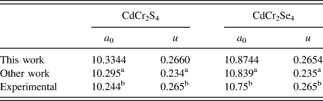
0 and the internal parameter u, the cell parameters and atomic positions were fully relaxed until a force convergence of 0.05 mRy/a.u. and an energy convergence of 10−4 Ry were reached. We found that the optimized lattice constants, a = 10.33 Å and a = 10.87 Å, overestimate the experimental value
Reference Hellwege18
by 0.88% and 1.15% for CdCr2S4 and CdCr2Se4, respectively, while optimized structure parameters values (u) are in good agreement with the experimental values. The lattice parameters obtained from present work and also with others work
Reference Wang, Gupta, Chshiev and Butler24
with the corresponding experimental values
Reference Hellwege18
are listed in Table I.
Calculated lattice constants, a 0, in Å and internal structure parameter, u, with experimental values for CdCr2X4 (X = S, Se).

b Ref. Reference Hellwege18.
III. RESULTS AND DISCUSSIONS
A. Electronic structure and DOS
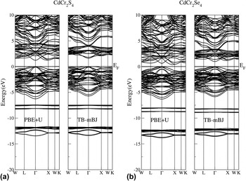
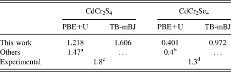
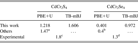
The electronic band structures for CdCr2S4 and CdCr2Se4 calculated using the PBE+U and TB-mBJ schemes are displayed in Figs. 1(a) and 1(b), respectively. The Fermi energy (E F) is at 0 eV. It is clear from Fig. 1(a) that the position of bands above E F is shifted to higher energies with TB-mBJ compared to the PBE+U scheme, while position of bands below E F remains almost same in both PBE+U and TB-mBJ schemes. The shifting of bands above E F is slightly prominent in CdCr2Se4 as compared to CdCr2S4 and can be easily identified in Fig. 1(b). We also found that in CdCr2S4 the valence band maximum (VBM) and conduction band minimum (CBM) is at Γ point for both schemes. Therefore a direct band gap of 1.218 eV and 1.606 eV is obtained by using PBE+U and TB-mBJ, respectively. In the case of CdCr2Se4, an indirect band gap is found to be 0.401 eV using the PBE+U scheme with VBM at Γ point and CBM between X and Γ point, while a direct band gap of 0.972 eV is obtained for the TB-mBJ scheme with VBM and CBM at Γ point. The value of band gaps is showing the semiconducting nature of both the materials which is in agreement with the earlier LSDA+U Reference Fennie and Rabe25 and simple GGA Reference Wang, Gupta, Chshiev and Butler24 results; however, the band gap values and energy bands have been predicted accurately only by the TB-mBJ scheme. The value of band gaps for CdCr2X4 (X = S, Se) calculated with PBE and TB-mBJ along with other works Reference Wang, Gupta, Chshiev and Butler24,Reference Fennie and Rabe25 and also with available experimental results Reference Sato, Sato, Furukawa and Nakajima42,Reference Zhao, Ren, Lupke, Hanbicki and Jonker43 are shown in Table II. Our calculated values of band gaps using TB-mBJ are comparable with the experiments.
Band structure of (a) CdCr2S4 and (b) CdCr2Se4 calculated by PBE+U and TB-mBJ schemes.

Band gap (E g) obtained by use of PBE+U and TB-mBJ with the experimental value for CdCr2X4 (X = S, Se) (all in eV).
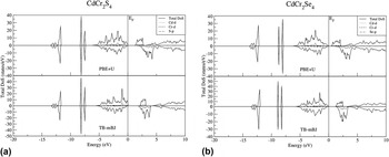
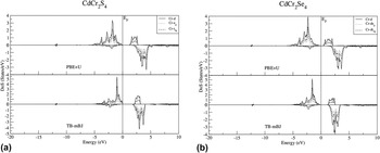
To visualize the electronic origin of band structures, total and atomic site projected DOS of CdCr2X4 (X = S, Se) are calculated using both schemes and displayed in Figs. 2(a) and 2(b). For CdCr2S4, the range of spin-up and spin-down valence band starts from −6.3 and −5.885 eV, respectively, up to E F the for PBE+U scheme. The spin-up conduction band is in the energy range from 1.218 eV to 2.958 eV, while spin-down conduction band is extended from 1.22 eV to higher energies. On the other hand in TB-mBJ scheme, the corresponding spin-up and spin-down valence bands lie at −5.73 and −5.49 eV up to E F. The spin-up conduction band is located in the range of 2.02–3.41 eV while spin-down conduction band is located in the range of 1.606–4.13 eV. In the case of CdCr2Se4, the spin-up and the spin-down valence bands are found at −6.36 eV and −6.02 eV, respectively, up to E F in the PBE+U scheme. The spin-up conduction band can be seen in the energy range of 0.401–2.61 eV, whereas spin-down conduction band starts from 0.53 eV and spreads to higher energies. In the TB-mBJ scheme, the spin-up and the spin-down valence bands are placed at −5.9 and −5.89 eV, respectively up to E F. The spin-up and the spin-down conduction bands are stretched from 1.15 and 1.11 eV, respectively, to higher energies. The spin-up valence band and the conduction band of total DOS of CdCr2X4 (X = S, Se) largely consist of Cr-d orbitals and to a smaller extent X-p orbitals in both the schemes. The spin-down valence band is a mixture of Cr-d and X-p orbitals with larger contribution from the latter. The spin-down conduction band mainly consists of Cr-d and X-p states with a larger contribution from the former. Empty Cr-d states above E F in the PBE+U scheme are shifted to higher energy in the TB-mBJ scheme. The splitting of empty and filled Cr-d states is more prominent in the TB-mBJ scheme than in the PBE scheme. This splitting is responsible for the larger band gap for CdCr2X4 in the TB-mBJ scheme. The asymmetrical nature of spin-up and spin-down states in total DOS confirms them to be magnetic compounds.
Total DOS and contribution of individual states of (a) CdCr2S4 and (b) CdCr2Se4 calculated by PBE+U and TB-mBJ schemes.

The crystal field splitting of Cr-d states in CdCr2X4 (X = S, Se) calculated by both the schemes is displayed in Figs. 3(a) and 3(b). For both the compounds, the octahedral field surrounding Cr-atoms split the Cr-d levels into t 2g and e g states with mixing between the two. The Cr-d levels are completely split between unfilled and filled states in both spin channels. It shows the semiconducting solution as observed experimentally. Reference Sato, Sato, Furukawa and Nakajima42,Reference Zhao, Ren, Lupke, Hanbicki and Jonker43 We also found that Cr-t 2g states are more dominating than Cr-e g states in up spin of VB and down spin of CB for both schemes. The larger band gap in TB-mBJ scheme for these compounds arises due to the pushing of Cr-e g and Cr-t 2g states of spin-up CB toward higher energy from E F.
Crystal field splitting of Cr-d states of (a) CdCr2S4 and (b) CdCr2Se4 calculated by PBE+U and TB-mBJ schemes.

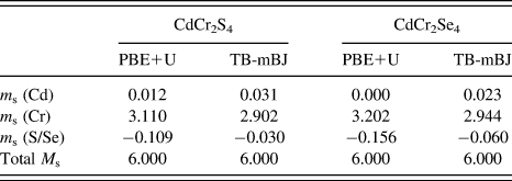
The atomic spin moment per atom (m s) and total magnetic moment per formula unit (M s) calculated for CdCr2X4 (X = S, Se) by PBE+U and TB-mBJ methods are shown in Table III. The total magnetic moment per formula unit (M s) for CdCr2X4 (X = S, Se) calculated by both the schemes is 6.00, which is consistent with that earlier reported. Reference Wang, Gupta, Chshiev and Butler24 Integer values of M s confirm these compounds to be half-metallic or semiconductor in nature. Reference Santos-Carballal, Roldan, Grau-Crespo and De Leeuw44
Atomic spin magnetic moment per atom (m s) and total spin magnetic moment (M s) per formula unit (in μB) calculated by PBE+U and TB-mBJ schemes.

B. Optical properties
Further we study the optical behavior of CdCr2X4 (X = S, Se) by use of the PBE+U and TB-mBJ schemes with spin–orbit interaction to determine their potential use in opto-electronic devices. We have adopted the electric dipole approximation in our optical calculations. The imaginary part of the dielectric tensor ε2(ω) Reference Wooten45 can be expressed as
 $${\varepsilon _2}(\omega ) = {8 \over {2\pi {\omega ^2}}}\int_{{\rm{BZ}}} {\sum\limits_{nn'} {{{{{\left| {{P_{nn'}}(k)} \right|}^2}{\rm{d}}{S_{\rm{k}}}} \over {\left| {\nabla {\omega _{nn'}}(k)} \right|}}} } \quad .$$
ε2(ω) depends on the joint DOS, ω nn′, and the momentum matrix element, P nn′. The real part ε1(ω) of the complex dielectric function can be calculated from the imaginary part ε2(ω) by using Kramers–Kronig (K–K) relation, Reference Wooten45
 $${\varepsilon _1}(\omega ) = 1 + {2 \over \pi }P\int_0^\infty {{{\omega '{\varepsilon _2}\left( {\omega '} \right)} \over {{{\omega '}^2} - {\omega ^2}}}} {\rm{d}}\omega '\quad ,$$
where P is the principal value of the integral. To calculate ε1(ω), we have calculated ε2(ω) up to 65 eV and have used this value as the truncation energy in the K–K relation to ensure convergence in the K–K transformation. Calculations of the reflectivity spectrum, frequency dependent refractive index n(ω) and the extinction coefficient k(ω) of CdCr2X4 (X = S, Se) have been performed by using the real part and imaginary part of the dielectric tensor.
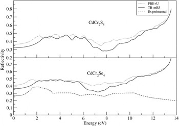
There have been reports of optical reflectivity measurements on CdCr2Se4. Reference Ohgushi, Okimoto, Ogasawara, Miyasaka and Tokura26 Reflectivity of CdCr2S4 calculated in this work by PBE+U and TB-mBJ schemes is shown in the upper panel of Fig. 4. Since the calculated dielectric tensor is same along the directions of lattice constants, the optical properties are isotropic in nature. Reflectivity stays low until 1.2 eV approximately for PBE+U and 1.6 eV for TB-mBJ, which are consistent with the energy gaps obtained by the use of the respective schemes. The larger band gap obtained by the use of the TB-mBJ scheme is responsible for the lower reflectivity in the low energy region compared with that obtained by the PBE scheme. Corresponding peaks and dips of the reflectivity spectra obtained by PBE+U scheme are shifted toward higher energy in the TB-mBJ scheme. The reflectivity spectrum in PBE+U scheme shows a broad structure between 1.2 and 7 eV followed by a dip at 7.49 eV. In TB-mBJ scheme, the broad structure is between 1.6 and 6.6 eV, followed by a dip at 7.71 eV. In the case of CdCr2Se4, reflectivity stays low till about 0.4 eV for PBE+U and 0.97 eV for the TB-mBJ scheme as shown in the bottom panel of Fig. 4 which is consistent with the energy gaps obtained by the use of the respective schemes. The reflectivity spectrum in PBE+U scheme shows a broad structure between 0.4 and 6.56 eV followed by a dip at about 6.78 eV. In TB-mBJ scheme the broad structure is between 0.97 and 6.13 eV. The calculated reflectivity by the TB-mBJ scheme is much closer in form to experimental spectrum than the PBE+U scheme in the lower energy range. The broad structures reported are mainly due to the transition from occupied Cr-d and X-p states to vacant Cr-d states.
Reflectivity of CdCr2X4 (X = S, Se) calculated by PBE+U and TB-mBJ potentials compared with available experimental data. Reference Ohgushi, Okimoto, Ogasawara, Miyasaka and Tokura26

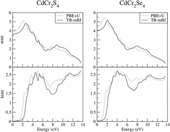
The left panel of Fig. 5 shows the calculated frequency-dependent refractive index, n(ω), and the extinction coefficient, k(ω), obtained by the use of the PBE and TB-mBJ schemes for CdCr2S4. The values of the static refractive index, n(0), given by PBE and TB-mBJ schemes are 4.05 and 3.63, respectively. The smaller value of n(0) given by the TB-mBJ scheme suggests that the refractive index at zero frequency is inversely related to the band gap of the material. In PBE+U scheme, n(ω) reaches a maximum peak of 5.09 at 2.13 eV followed by a dip at 6.92 eV. In TB-mBJ scheme, n(ω) reaches a maximum peak of 4.83 at 2.62 eV followed by a dip at 6.65 eV. Lack of structures at higher energies suggests that beyond a particular energy, the material can no longer act as a transparent material and starts to absorb high-energy photons beyond that energy. The main peaks observed at about 3.74, 5.07, and 6.0 eV for k(ω) followed by a dip at 7.57 eV in the PBE+U scheme are shifted toward higher energy at around 4.55, 5.34, 6.05, and 7.82 eV respectively in the TB-mBJ scheme causing the rapid attenuation of light in this energy range. The right panel of Fig. 5 shows the calculated refractive index, n(ω), and the extinction coefficient, k(ω), obtained by the use of the PBE and TB-mBJ schemes for CdCr2Se4. The values of the static refractive index, n(0), given by PBE and TB-mBJ schemes are 4.56 and 4.03 respectively. Again, here also the larger band gap obtained by the use of the TB-mBJ scheme causes the lower reflectivity in the low energy region compared with that obtained by the PBE scheme. In PBE+U scheme, n(ω) reaches a maximum peak of 5.43 at 1.42 eV. In TB-mBJ scheme, n(ω) reaches a maximum peak of 5.17 at 2.1 eV. Lack of structures at higher energies suggests that the material can no longer act as a transparent material and starts to absorb high energy photons beyond a specific energy. The main peaks observed at about 3.68 and 4.8 eV for k(ω) in the PBE+U scheme are shifted toward higher energy at about 4.04 and 4.66 eV, respectively, in the TB-mBJ scheme, causing the rapid attenuation of light in this energy range.
Refractive index, n(ω), and extinction coefficient, k(ω), of CdCr2X4 (X = S, Se) calculated by PBE+U and TB-mBJ schemes.

IV. CONCLUSIONS
Electronic and optical properties of CdCr2X4 (X = S, Se) normal spinels by using the PBE+U and TB-mBJ schemes have been performed. The calculated energy band structures show a direct band gap for CdCr2X4 in the TB-mBJ scheme. The larger splitting of Cr-d states is responsible for the larger band gap in the TB-mBJ scheme. The asymmetrical nature of spin-up and spin-down states in total DOS confirms them to be magnetic compounds. Integer values of total magnetic moment per formula unit indicate these compounds to be half-metallic or insulators. The larger band gap obtained by the use of the TB-mBJ scheme causes lower reflectivity in the low energy region compared with that given by the PBE scheme. The smaller value of n(0) and k(0) obtained by TB-mBJ scheme suggests a larger band gap of the materials. The band gap and the optical properties calculated by TB-mBJ functional agree more with the existing experimental data, which makes it better suited to study the electronic structure of CdCr2X4.