I. INTRODUCTION
Silicon nitride thin films are commonly used as a structural material for microelectromechanical systems (MEMS).Reference Ouacha, Willander, Hammarlund and Logan1–Reference Santana, Fandino, Ortiz and Alonso3 Among the commonly used chemical vapor deposition techniques, plasma-enhanced chemical vapor deposition (PECVD) is preferred over low-pressure chemical vapor deposition in the fabrication of MEMS devices that utilize temperature-sensitive materials, such as those integrated on group III–V and II–VI semiconductors.Reference Antoszewski, Martyniuk, Musca, Dell and Faraone4, Reference Winchester and Dell5 The extra energy supplied by the plasma in the PECVD process allows for low-temperature deposition of thin films.
The process of PECVD synthesis of thin films, in particular SiNx thin films, involves complex chemical reactions in the plasma system. These reactions often involve extensive bond scrambling and are often incomplete, particularly at low deposition temperatures. Consequently, these films are often found to be amorphous, chemically nonstoichiometric to bulk Si3N4, and contain substantial amounts of bonded hydrogen.Reference Soh, Savvides, Musca, Martyniuk and Faraone6–Reference Karcher, Ley and Johnson8 As a result, these films have been found to be chemically and physically unstable in certain environmental conditions.Reference Knolle and Osenbach9–Reference Jehanathan, Liu, Walmsley, Dell and Saunders12 Changes in chemical and physical structures will have direct impact on the properties, subsequent performances, and long-term reliability of the MEMS devices that use these films. Therefore, it is of critical importance to study the environmental stability of these films and to understand their physical integrity. This article reports on the thermal damages of PECVD SiNx films caused by heating to elevated temperatures in air.
II. EXPERIMENTAL METHODS
SiNx films were deposited on 100-μm-thick (100) single-crystal Si wafers by means of PECVD using a 13.6-MHz Oxford Instruments PECVD 80 system (Oxford Instruments Plasma Technology, Bristol, UK). The wafers were cleaned in acetone, methanol, and iso-propanol before deposition. The process gases for the deposition were ultra-high-purity grade SiH4, NH3, and N2. Two films were deposited at deposition temperatures of 448 K and 573 K.
The SiNx films synthesized were ∼1.2-μm thick. The films were heated in air for 1.8 ks at various temperatures up to 1373 K. The heating was conducted by inserting a sample into the furnace that has been preheated to the set temperature. Surface morphologies of the films were examined using a Zeiss 1555 SUPRA field emission scanning electron microscope (SEM, Carl Zeiss, Oberkochen, Germany). Cross-section samples were prepared by means of focused ion beam (FIB) milling using an xT Nova Nanolab 200 (FEI, Hillsboro, OR). Chemical structure of the films was characterized by means of Fourier transform infrared spectroscopy (FTIR) at room temperature using a Sopra GES5 Spectroscopic Ellipsometer (Sopralab, Courbevoie, France).
III. RESULTS AND DISCUSSION
A. Morphological damages
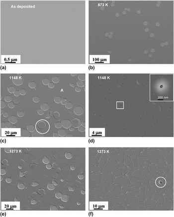
Figure 1 shows a series of SEM micrographs of the surface morphologies of a SiNx film. The film was deposited at 448 K and was 1100-nm thick. The images were taken from a few samples, which had been heat treated at different temperatures in air for 1.8 ks prior to the observation. Each image shown is from a different sample. Fig. 1(a) shows an as-deposited film. The film surface was smooth without any sign of defects to the resolution of the SEM (∼5 nm). Figure 1(b) shows a sample heated at 873 K. The sample was found to have developed a population of nearly perfect circular craters. The sizes of the craters ranged from 30 to 70 μm. Figure 1(c) shows a sample heated to 1148 K. It is seen that the population of the circular craters had increased and the sizes of the craters, appearing in between 10 and 30 μm, had decreased. These craters were found to be formed by penny-shaped disks of the film fractured off the surface, as evident in the micrograph in the circled area. These circular craters are referred to as “penny cracks.” Figure 1(d) shows a detailed view of the surface of the film in a similar area indicated by “A” in Fig. 1(c). It is seen that the film developed uniformly dispersed dark dots, which are identified to be small pinholes. The inset in Fig. 1(d) shows a pinhole at a higher magnification from an area indicated by the white rectangle. The pinholes are <100 nm in size. Figure 1(e) shows a sample heated to 1273 K. This sample exhibited fewer penny cracks compared with the sample heated to 1148 K but more roughened and damaged surface. Figure 1(f) had been heated to 1373 K. This sample exhibited massive uniformly distributed random cracks, referred to as “dry mud” cracks. In addition, very few small pockets of crystals were observed, as indicated in the circled area.
Morphology of plasma-enhanced chemical vapor deposition (PECVD) SiNx films deposited at 448 K and subsequently heat treated to different temperatures up to 1373 K for 1.8 ks.

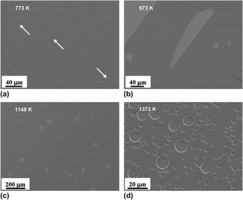
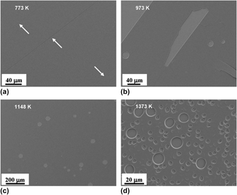
Figure 2 shows a selection of SEM images of the surface morphologies of a film deposited at 573 K. The as-deposited film showed similar “featureless” morphology to that shown in Fig. 1(a). Figure 2(a) shown in Fig. 2 is for a sample heated to 773 K. The sample was found to exhibit some long straight-line cracks, mostly parallel in a few self-defined directions. Figure 2(b) shows a sample heated to 973 K. This sample shows more extensive line cracks and some spalling of large pieces from the substrate. Occasionally, some penny cracks were also seen. Sample (c) was heated to 1148 K. This sample developed more penny cracks but no thin-line cracks. The sizes of the penny cracks were similar to those observed in the film deposited at 448 K, but the population was much lower, as evident in the comparison with Fig. 1(c). Sample (d) was heated to 1373 K. This sample exhibits a high population of small “pits,” ∼3 μm in size, in coexistence with some penny cracks, which were just under 10 μm in size. Close examination indicates that each pit is actually a nest of small crystals of ∼100–300 nm in size [as shown in Fig. 5(a)]. The film also contains pinholes and random cracks.
Morphology of PECVD SiNx films deposited at 573 K and subsequently heat treated to different temperatures up to 1373 K for 1.8 ks.

These observations are unique in the literature. Some other but similar forms of physical damages have been reported in the literature for other thin film materials. Cordill et al. analyzed “telephone cord” shaped delamination buckling of compressively stressed tungsten thin films.Reference Cordill, Bahr, Moody and Gerberich13 Coupeau et al. conducted similar analysis on circular buckling blister of Au thin film on Si substrate.Reference Coupeau, George, Regache, Colin and Grilhe14 The most relevant observations are reported by Hughey and Cook.Reference Hughey and Cook15 In their work, they observed circular blistering of severely compressively stressed PECVD SiNx thin films caused by thermal cycling. The formation of these blisters has been attributed to the release of bonded hydrogen and the compressive stresses existing in the films.
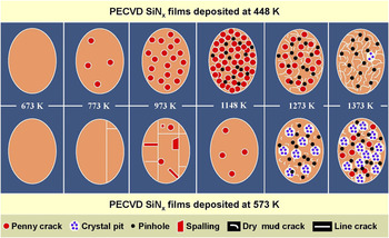
Figure 3 shows a schematic expression summarizing the types of the thermally induced morphological damages and the temperature regimes of the damages observed in the two films. It is generally found that the film deposited at 573 K is more resistant to heating than the film deposited at 448 K. The low-temperature film exhibited more penny cracks and dry mud cracks, whereas the high-temperature film exhibited much more extensive crystallization.
Overview of the thermal damages of PECVD SiNx deposited at 448 K and 573 K.

B. Chemical damages
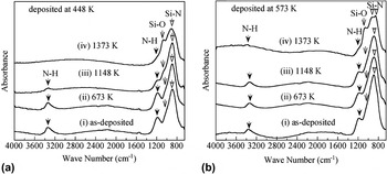
Figure 4 shows the FTIR measurements of the two SiNx films. The spectra shown in (a) are for the film deposited at 448 K, and those shown in (b) are for the film deposited at 573 K. Sample (i) in each figure was in the as-deposited state. The as-deposited films contained high populations of Si–N bonds and N–H bonds and trace amounts of Si–O bonds. Samples (ii), (iii), and (iv) have been heat treated in air for 30 min at 673, 1148, and 1373 K, respectively. It is seen that heating in air has led to progressive loss of N–H bonds, weakening of the intensity of Si–N bonds, and the appearance and strengthening of the intensity of Si–O bonds. These measurements demonstrate that the PECVD SiNx films were actually SiNxHy films and that heating in air to elevated temperatures causes oxidation of the films at the expense of their N and H contents. A detailed analysis of the chemical changes has been reported elsewhere.Reference Jehanathan, Liu, Walmsley, Dell and Saunders12, Reference Jehanathan, Walmsley, Liu and Dell16 It has been found that the original SiNxHy exists in a structure conforming to a “random bonding” model and that oxidation leads to the decomposition of the matrix to a “random mixing” structure of amorphous SiNx and crystalline SiO2.Reference Aydinli and Ay17–Reference Ray, Das, Maiti, Lahiri and Chakraborti19
FTIR spectra for SiNx films deposited at (a) 448 K and (b) 573 K; subsequently heat treated at temperatures up to 1373 K for 1.8 ks.

It has also been generally observed that the film deposited at 448 K is less oxidation-resistant and contains a higher concentration of hydrogen than the film deposited at 573 K. This is consistent with previous studies.Reference Santana, Fandino, Ortiz and Alonso3
C. Crystallization
Figure 5 shows SEM images of the crystals formed. Figure 5(a) shows a detailed view of a crystal pit from the same sample shown in Fig. 2(d). The white particles appearing at the bottom of the pit are small, equiaxial, and multiple faceted crystals of 100–300 nm in size. The dark spots appearing with the white crystals are empty pockets left behind by some crystals that had dropped out. The pit appears to be significantly larger in volume than the crystals, implying a significant missing volume.
SEM images of the crystals formed in the matrix of SiNx.

Figure 5(b) shows an SEM image of the cross section of a SiNx film deposited at 448 K and subsequently heat treated to 1148 K. The cross-section sample was prepared by FIB. The Pt and Au layers on the top are the working layers coated after the heat treatment for FIB processing and are not part of the original sample. The dashed horizontal line marks the boundary between the SiNx film and the Si substrate. The micrograph reveals two hidden crystals formed inside the body of the film. It is evident that large cavities are formed around these crystals. Energy-filtered transmission electron microscopic analysis indicates that the crystals contain only Si and N, whereas the surrounding matrix contains Si, Ni, and low level of O.Reference Jehanathan, Saunders, Liu and Dell20 Electron diffraction analysis indicates that the crystals have a hexagonal structure similar to β-Si3N4.Reference Jehanathan, Saunders, Liu and Dell20
D. Damage mechanisms
It is seen that the amorphous PECVD SiNx films experience physical, chemical, and structural damages during heating to elevated temperatures in air. The chemical damage is mainly in the form of oxidation, at the expense of N and H contents of the films. The structural damages include crystallization of the amorphous SiNx matrix to β-Si3N4. The physical damages are in multiple forms, including the penny cracks, pinholes, random dry mud cracks, line cracks, and spalling. From the evidences collected in this study, the line cracking and spalling are considered specific cases related to the particular conditions of the samples tested. The pinholes are possibly related to the loss of the N and H contents at high temperatures in air; but the current study does not provide more information to enable a convincing identification of its possible mechanisms.
The penny cracks have been found to form by circular buckling or circular blistering. Such failure mode implies compressive in-plane stresses. The circular shape implies that the compressive stresses in-plane isotropy. The random cracks are typical of the morphology of cracking under the influence of in-plane tensile stresses. It is commonly considered that internal stresses, mostly thermal stresses, cause film fracture and delamination.Reference Hughey and Cook15, Reference Audoly21 In comparison, little attention is paid to the effect of possible changes in chemical structure of the films. It is evident that heating to elevated temperatures causes oxidation of the amorphous SiNx into crystalline SiO2 at relatively lower temperatures and the crystallization of the amorphous SiNx into Si3Ni4 at the higher temperatures, i.e.,


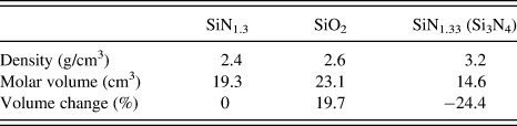
The PECVD SiNx films used in this study, with an approximate atomic ratio of SiN1.3,Reference Jehanathan, Walmsley, Liu and Dell16 have a density 2.4 g/cm3.Reference Walmsley, Liu, Hu, Bush, Winchester, Martyniuk, Dell and Faraone22 The volume changes of the above two reactions are estimated as summarized in Table I.
Volume changes of SiNx due to oxidation and crystallization.
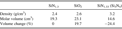
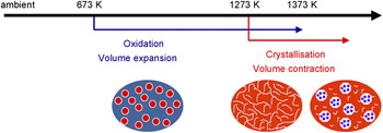
It is seen that the oxidation of SiNx to SiO2 is associated with a volume expansion of 19.7%, whereas the crystallization of amorphous SiNx to Si3Ni4 is associated with a volume contraction of 24.4%. It needs to be pointed out that these volume changes are estimated for the complete conversion of the reactions. In reality, the reactions are highly incomplete. Such volume changes are consistent with the forms of cracking observed in the respective temperature ranges. Figure 6 shows a schematic illustration of the mechanisms of cracking damages of the films.
Cracking mechanisms of PECVD SiNx films.

In addition, it is also expected that the oxidation process is time-dependent, whereas in contrast the crystallization is more a temperature-dependent process. This condition is critical for the cracking of the films heated to above 1273 K, in which dry mud cracks are observed. In this case, the fast heating the samples through the intermediate temperature range does not provide enough diffusion time for oxidation, thus the build-up of excessive compressive stresses to cause the formation of the penny cracks. This expectation is also consistent with the observation that the high-temperature deposited PECVD SiNx film is more chemically stable and oxidation resistant, thus lower extent and higher temperatures of penny cracking, than the low-temperature deposited film.
IV. CONCLUSIONS
PECVD SiNx films are subjected to various mechanical, structural, and physical damages when heated to elevated temperatures in air. These damages occur in different temperature ranges. The type and extent of the damages are also dependent on film deposition conditions. The film deposited at 573 K is more chemically stable and more damage resistant compared with the film deposited at 448 K.
The chemical damages include the loss of N and H contents and the oxidation of the SiNxHy films. The structural damages include the crystallization of amorphous SiNx matrix. The physical damages include pinholes, penny cracks, random cracks, line cracking, and spalling. Line cracking and spalling are considered individual cases particular to the specific samples. The current study does not offer possible explanation of the reasons for the formation of the pinholes.
The formation of the penny cracks is attributed to in-plane compressive stresses, which are in turn attributed to the oxidation of the SiNx matrix. The formation of the dry mud cracks is attributed to in-plane tensile stresses, which are in turn attributed to the loss of the N and H contents and the crystallization of the SiNx matrix.
ACKNOWLEDGMENTS
This work is financially supported by ARC Grant DP0559744. The authors acknowledge the experimental support of the Centre for Microscopy, Characterization and Microanalysis of the University of Western Australia. The financial support from the ARC Network of Nanotechnology is also acknowledged.