Introduction
It is well established that electrical fields (DC and AC) affect ionic conduction and diffusion transport in ceramics in a significant way.[Reference Narayan, Weeks and Sonder1–Reference Tsang and Chen4] Narayan and co-workers (ORNL researchers) in the late 70s and early 80s[Reference Narayan, Weeks and Sonder1–Reference Tsang and Chen4] studied extensively the characteristics of electrical conductivity in pure (ORNL) and impurity doped (Norton) MgO single crystals as a function of temperature and applied field, and analyzed the role of defects and impurity clusters in enhancing electrical conductivity and mass transport which led to an avalanche and thermal electric breakdown. These studies established the presence of high concentrations of intrinsic (anion and cation vacancies) defects and impurity precipitates in highly conductive regions between the electrodes after cooling. The enhancement of conductivity at high temperatures exhibited an avalanche effect, which, if uncontrolled by limiting the current flow, led to melting and eventually evaporation of materials between the electrodes. These results suggested a predominant role of vacancies and impurities in electronic conduction and diffusion transport.
Although ORNL work was conducted at higher fields (>1000 V/cm) and higher temperatures (>1000 °C), other researchers[Reference Yang and Conrad5–Reference Francis and Raj15] have obtained interesting results on mechanical properties and sintering at lower fields, which can be correlated with earlier results at higher fields. At lower fields Conrad and co-workers have found interesting effects on polycrystalline NaCl, MgO, and yttria stabilized zirconia materials related to grain growth retardation and reduction in flow stress and enhancement in ductility.[Reference Yang and Conrad5–Reference Conrad and Yang8] Applied electric (AC and DC) fields have been shown to produce a host of interesting phenomena related to sintering of solid-state materials.[Reference Groza and Zavaliangos9–Reference Francis and Raj15] More recently Raj and coworkers[Reference Raj, Cologna and Francis13–Reference Cologna, Rashkova and Raj16] have shown that the application of DC electrical fields in the intermediate range of about 30–100 V/cm produced sintering of polycrystalline yttria-stabilized zirconia in mere seconds at furnace temperatures of 850 °C, well below the normal sintering temperatures of around 1450 °C.[Reference Cologna, Rashkova and Raj16] Remarkably, these field-treated samples did not exhibit grain growth. In a recent paper,[Reference Narayan17] the author proposed a unified mechanism to explain the critical elements of the field-assisted phenomena ranging from reducing the flow stress to lowering the overall effective sintering temperatures of materials. I also proposed a new grain growth model to take into account defect generation under field-assisted conditions and explained reduction in grain growth rate, the rate eventually going to zero.[Reference Narayan18]
In this paper, I focus on selective melting of grain boundaries as a result of field assisted generation of defects and their segregation at grain boundaries. Defect generation is enhanced via field-assisted electron trapping by cations and it is further enhanced in the presence of impurities which can trap electrons and create charge imbalance. Electrical-field induced creation of defects has interesting parallels with pulsed laser annealing, internal reduction, and vaccum annealing.[Reference Mal, Yang, Gupta, Prater and Narayan19, Reference Gupta, Dutta, Mal and Narayan20] The field-induced defects interact with and segregate at dislocations and grain boundaries, leading to higher currents and joule heating along grain boundaries which further enhance the concentration of defects. This leads to an avalanche and melting of grain boundary regions. This process, which I refer to as selective-melt sintering, can lead to fully dense grain boundary regions in a short time, as diffusivities in liquid state (10−4 to 10−5 cm2/s) are substantially higher (6–10 orders) than those in solid state at normal sintering temperatures.
In the following, I discuss critical issues related to field-assisted sintering, leading to selective grain boundary melting and the process of selective-melt sintering (SMS). The results and discussion are divided into five components related to field-assisted generation of defects, segregation of defects and impurities at dislocations and grain boundaries, role of defects in mechanical property modification and grain growth retardation, selective joule heating and melting of grain boundaries, and selective melt sintering.
Field-assisted generation of defects
When ceramics (wide bandgap materials) are subjected to a field at high temperatures, there is some thermal generation of free carriers, depending upon the bandgap, trap density (defects), dopant concentration and the position of the Fermi level. The applied field transports these free electrons, which can be trapped by cations and defects such as anion vacancies. The electron trapping by cations (Mn+ → M(n−1)+) leads to internal reduction and creation of anion vacancies. The formation and the concentration of M(n − 1)+ defects is controlled by Gibbs free energy ΔG 0(T) = –RT ln C(n−1)+/Cn+/n e, where C(n−1)+ is the concentration of reduced cations, Cn+ is the original cation concentration which can be close to unity, and n e is the concentration of free electrons. Thus, the availability of free electrons is critical for driving this reaction, which can be induced by the presence of midgap states in wide bandgap materials. This electron trapping can lead to formation of M0 defects eventually (Mn+ → M(n−1)+ → M0), which can cluster to form metallic precipitates. These reduced cations often get kicked into interstitial sites, leaving behind cation vacancies. Thus, the applied field promotes electron trapping, which generates anion and cation vacancies, and M0 defects, which cluster to form metallic precipitates. Certain impurities, such as yttrium in zirconia and nickel in magnesium oxide, provide more efficient traps and enhance the generation of defects and formation of metallic precipitates. It is interesting to note that this reduction process induced by the applied field is equivalent to high-temperature annealing in vacuum and pulsed laser annealing.[Reference Mal, Yang, Gupta, Prater and Narayan19, Reference Gupta, Dutta, Mal and Narayan20]
Segregation of defects and impurity precipitation at dislocations and grain boundaries
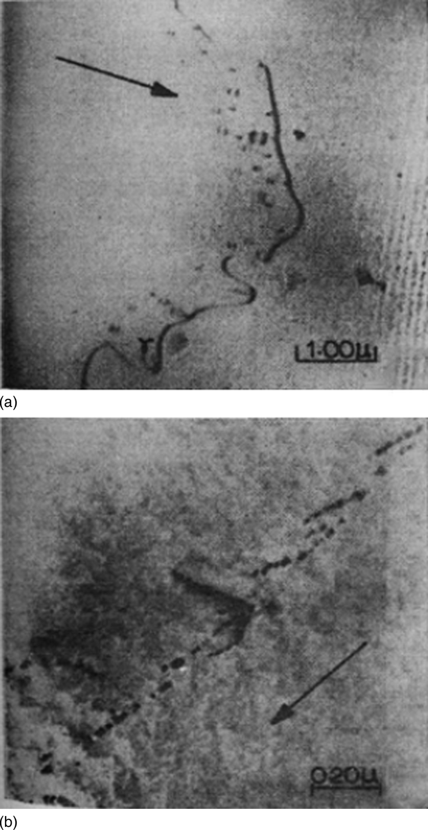
As discussed above, the applied field primarily generates anion and cation vacancies, in addition to electron trapped M(n−1)+ → M0 cation and impurity defects. The neutral defects can get into interstitial sites with lower activation energy for diffusion and cluster to form metallic impurity precipitates. These cation and anion vacancies and M0 defects can interact with the dislocations and grain boundaries through elastic and electronic (space charge) potentials. The detailed studies on segregation of defects at dislocations showed the formation of vacancy loops around dislocations, as shown in Fig 1(a), where vacancy loops of a〈100〉 Burgers vector are preferentially associated with an edge a/2〈110〉 edge dislocation. In MgO, which has an NaCl structure, the formation of 〈100〉 dislocation loops can occur only as a result of clustering of vacancies.[Reference Narayan21] The average size of these dislocations was found to be 50 nm (500A) and number density 1.0 × 1014 cm−3. From the number density and average size of the loops, the density of point defects was determined to be 1.0 × 1019 cm−3. Assuming the formation energy of vacancy to be around 4.0 eV, local temperature around dislocations from which defects are quenched is estimated to be of the order of 3000 K. It is interesting to note that the vacancy dislocation loops lie only on one side as expected for an edge dislocation, which has a compressive stress field above the half-plane and a tensile stress below the half-plane.
(a). Bright-field electron micrograph under kinematic diffraction conditions optimized for strain contrast (Bragg deviation parameter ω = 0.6), showing mostly a〈100〉 loops and occasionally γ a/2〈110〉 loops near an edge dislocation. The arrow indicates the direction of diffraction vector [200]. (b) Bright-field electron micrograph under kinematic diffraction conditions optimized for strain contrast (Bragg deviation parameter ω = 0.6). The arrow indicates the direction of the diffraction vector [200].

The results on grain boundaries after the field treatment show that the point defects have been absorbed by a dislocation climb, and there is a high density of impurity precipitates (as shown in Fig.1(b)) whose average size and number density were estimated to be 10 nm (100A) and 2.5 × 1015 cm−3, respectively. These results from field-treated samples clearly established the role of high density of intrinsic anion and cation vacancies and a small fraction of interstitials in addition to impurities, which were present in small amounts both in ORNL and nominally pure Norton MgO crystals. It should be noted that these segregation effects of intrinsic defects and impurities are observed only in field-treated samples, they disappear on subsequent thermal annealing without the applied field. Also, such segregation effects are not observed in samples quenched from high temperatures in the absence of applied field. The defect segregation is controlled by the interaction energy ΔU of a point defect with an edge dislocation, which is given by
 $$\Delta U = - \left[{\left({1+\nu } \right)\mu b/\left({1-\nu } \right)3\pi \Delta V} \right]{\rm Sin} \theta /r{\rm\comma \; }$$
where ν is the Poisson's ratio, b is the Burgers vector, μ is the shear modulus, ΔV is the volume change with respect to the host atom, r is the distance between the point defects and the dislocations, and θ is the angle between the x-axis and the r-vector. Thus, undersize impurity and vacancy defects with negative ΔV should segregate on the compressive side above the dislocation core, and oversize impurity and interstitial defects on the tensile side below the dislocation core.[Reference Narayan and Holland22] Using μ = 1.49 × 10¹² dynes/cm2 and ν = 0.173, and b = 4.23A for MgO, the maximum value of σ H at 100A from the dislocations is estimated to be 1010 dynes/cm2, which is a substantial interaction energy on point defects exerted by the dislocations. Since this interaction energy varies as (1/r), its influence can extend up to 500A, as observed experimentally.
Selective Joule heating and melting of grain boundaries
It is argued that application of the electrical field assists the generation of defects, where the electrons take part in the reduction of cations, and this reduction process (Mn+ → M(n−1)+ → M0) eventually results in the formation of M0 defects which are kicked into interstitial sites.[Reference Narayan21] The concentration of M0 defects is determined by the efficiency of electron trapping and the gain in free energy ΔG (= –RT ln K), where K is the reaction constant. These defects can migrate rapidly and contribute to electronic conduction and are also responsible for the formation of metallic impurity precipitates upon cooling. These M(n−1)+ and M0 defects segregate preferentially at the dislocations and the grain boundaries through elastic interaction. This field-induced reduction creates anion vacancies and these anion vacancies can trap electrons, leading to V −(V 0 → V −) defects.[Reference Narayan, Chen and Moon23] This trapping of electrons is known to reduce migration energy of vacancies. These defects segregate at dislocations and grain boundaries through elastic and electronic interactions. The preferential ionic and electronic conduction along dislocations and grain boundaries results in selective joule heating, which can lead to an avalanche heating and selective melting of grain boundary regions.
Role of defects in mechanical properties and grain growth retardation
The segregation and field-assisted migration of defects around dislocations and grain boundaries causes enhanced ionic and electronic conduction, which leads to selective joule heating. The selective joule heating of dislocations enhances their mobility and reduces the flow stress. The temperature dependence of strain rate  $\dot \Upsilon $ can be expressed as[Reference Hirth and Loathe24]
 $$\dot \Upsilon = \rho b\nu _{\rm d} s\; {\rm exp}\left({-\Delta G/kT} \right)\comma \;$$
where ρ is the mobile dislocation density, b is the magnitude of Burgers vector of dislocation, ν d is the frequency of vibration of the dislocation segment involved in thermal activation, and s is the average distance to which the dislocation moves after the successful jump. The presence of defects and joule heating increase the dislocation mobility and reduce the flow stress.[Reference Conrad and Yang7, Reference Conrad and Yang8] This reduction will saturate once all the impurities are reduced and the supply of vacancies is exhausted.[Reference Narayan17, Reference Narayan18]
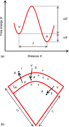
The field-assisted generation and segregation of defects at grain boundaries retards grain growth by promoting inverse vacancy jumps and reducing the thermodynamic driving force for grain growth, as shown in Fig. 2. Considering both kinetic and thermodynamic factors under field-assisted conditions, we derived for grain growth rate as[Reference Narayan18]
 $$\displaystyle{{{\rm d}r} \over {{\rm d}t}}=f\lambda c_{\rm V} \nu _{\rm D} \exp \left({ - \displaystyle{{\Delta \dot G} \over {kT}}} \right)\left[{1 - \exp \left({+\displaystyle{{\Delta G} \over {kT}}} \right)} \right]\comma \;$$
where C v is the vacancy concentration, νD is the Debye frequency, f is the geometrical factor for vacancy jumps,  $\Delta \dot G$ is the activation barrier for vacancy diffusion across the boundary and ΔG is the gain in free energy as shown in Fig. 2, which should be negative for the reaction to proceed.
(a). Change in free energy with distance across the grain boundary with jump distance, λ. (b) Vacancy jumps (for vacancy-atom exchange) across the interior (radius r i) and exterior (radius r e) of a grain boundary.
The grain growth rate has two terms, first fλc Vν Dexp (−(ΔG/kT)) is the kinetic or diffusion term and the second [1 − exp(+(ΔG/kT))] is the thermodynamic term, which is associated with phase transformation or gain in energy with the movement of the grain boundary.
Assuming ΔG = kT, we can write the grain growth rate as
 $$\displaystyle{{{\rm d}r} \over {{\rm d}t}}=f\lambda c_{\rm V} \nu _{\rm D} \left({\displaystyle{{ - \Delta G} \over {kT}}} \right)\exp \left({ - \displaystyle{{\Delta \dot G} \over {kT}}} \right).$$
The field-assisted defect segregation at grain boundaries promotes inverse vacancy jumps against grain growth, as shown in Fig. 2 (step 3). In addition, thermodynamic driving force ΔG is reduced with applied field and it can be driven to zero during the melting of grain boundaries. When there is a first-order phase transformation such as melting, the free energy at the melting point is zero and the grain growth rate will be driven to zero. Below the melting point ΔG = ΔS mΔT, where ΔS m is the change in entropy and ΔT is the undercooling. This thermodynamic driving force will make external and internal melt boundaries move toward each other resulting in zero net grain growth, as observed by Raj and co-workers.[Reference Cologna, Rashkova and Raj16]
Grain boundary melting and selective melt sintering
The most interesting aspect of the applied field is that defect segregation and an avalanche in field-assisted transport can lead to selective melting of grain boundaries while the bulk of the material within the grains is at a much lower temperature. Thus, the selective-melt sintering can lead to a huge reduction in energy for materials processing. The γ p ratio of energy consumption under SMS to normal sintering can be estimated by
 $$\gamma _{\rm p}=T_{{\rm SMS}} /T_{\rm N}+3\delta _{{\rm gb}} /d\left({1 + L_{\rm m} /T_{\rm m} C_{\rm v} } \right)\comma \;$$
where δ gb is the width of the grain boundary melted region, d is the grain size, L m is the latent heat of fusion melting, T m is the melting temperature, C v is the specific heat, T SMS is the reduced temperature for sintering and T N is the normal sintering temperature. Raj and co-workers have shown a drastic reduction in sintering temperature from 1450 to 850 °C in 3 mole% yttria stabilized zirconia[Reference Cologna, Rashkova and Raj16] with an applied field of 40 V/cm. Using L m = 700 J/g, C v = 420 J/gK, and T m for 3YSZ as 2823 K, we obtain a drastic 40% reduction (for grain size, d = 60 nm, assuming δ gb = 4 nm in Eq. (4)) in energy consumption in materials processing by selective-melt processing. Since diffusivities in the liquid state are substantially higher (6–10 orders) than those in the solid state at normal sintering temperatures, fully dense materials are obtained in a much shorter time. Since melting involves a first-order phase transformation, all the porosity and impurities are redistributed rapidly in the liquid phase, giving the appearance of clean boundaries.[Reference White, Narayan and Young25]
In summary, the applied electrical field assists generation anion and cation vacancies and promotes reduction of cations and impurities. The generation of defects is greatly enhanced by impurities which trap electrons supplied by the applied field. Upon cooling, these vacancies cluster into dislocation loops and impurities into precipitates. Enhanced defect segregation coupled with field-assisted current flow leads to selective joule heating of dislocations and grain boundaries. The primary mechanism for selective joule heating of dislocations and grain boundaries is the segregation and transport of defects which are generated as a result of the applied field. These effects reduce flow stress and retard grain growth in the solid state. The selective joule heating, if not controlled by limiting the current flow, generates more defects and sets up an avalanche resulting in selective and localized melting of grain boundaries, while keeping the bulk of the grain at a much lower temperature. This selective melting removes porosity at grain boundaries and provides more efficient sintering due to first-order phase transformation and fast diffusivities (10−4 to 10−5 cm2/s) in the liquid. We refer to this sintering mode as selective-melt sintering, which can occur at lower overall temperatures with much lower energy consumption compared with the conventional sintering involving solid-state diffusion.
Acknowledgements
The author is pleased to acknowledge useful discussions and comments on the manuscript by Professor Hans Conrad.