I. INTRODUCTION
Lead telluride (PbTe,  , a = 0.64 nm) has been recognized as one of the best thermoelectric materials since the 1960s.Reference Greig1, Reference Lyden2 Normally, the maximum thermoelectric dimensionless figure-of-merit (ZT) of bulk PbTe is around 0.8–1.0 at ~650 K.Reference Snyder and Toberer3, Reference Kanatzidis4 Recently, by nanostructuring and alloying (elemental substitution), the ZT values of PbTe-based thermoelectric materials have been dramatically increased to 1.5 at ~650 K.Reference Kanatzidis4–Reference Zhou, Li and Kita7 All those researchersReference Kanatzidis4–Reference Zhou, Li and Kita7 reported the findings of various nanostructures: nanoinclusions,Reference Kanatzidis4 nanodots,Reference Hsu, Loo, Guo, Chen, Dyck, Uher, Hogan, Polychroniadis and Kanatzidis5 nanoscale domains,Reference Poudeu, Angelo, Downey, Short, Hogan and Kanatzidis6 or nanoscopic inhomogeneities,Reference Zhou, Li and Kita7 and they believed that these nanoinclusions (3–20 nm)Reference Kanatzidis4 led to stronger phonon scattering, which caused the reduction of the lattice thermal conductivity and ultimately the increase in the ZT value of the PbTe-based thermoelectric materials. However, as pointed out by Kanatzidis,Reference Kanatzidis4 considerably more characterizations are required to fully understand the nanoinclusions, which are endotaxially embedded in the PbTe matrix. More specifically, the origin of the nanoinclusions, which is a key feature of the bulk nanostructured PbTe-based thermoelectric materials,Reference Kanatzidis4 remains unclear.
To study the formation mechanism of the nanoinclusions, we have carried out extensive transmission electron microscopy (TEM) experiments on the nanostructure of the PbTe and PbTe-related materials. To our surprise, we discovered that the nanoinclusions, as thought before, are nothing but strain fields (3–20 nm) caused by Pb-depleted disks (2–5 nm in diameter, less than 0.5 nm in thickness, and 9 × 1017 cm−3 in volume density) lying on the {001} planes. These strain fields generate TEM bright-field contrast images closely resembling those of the reported nanoinclusions in size, shape, distribution, and orientation.Reference Kanatzidis4–Reference Zhou, Li and Kita7 Furthermore, it is known that both the Pb-depleted disks (coherent interfaces) and the lattice strain fields play an important role in phonon scattering, which is the original reason for the significant reduction in lattice thermal conductivity with only a small impact on electrical conductivity.Reference Hsu, Loo, Guo, Chen, Dyck, Uher, Hogan, Polychroniadis and Kanatzidis5
Even though the crystal imperfections have been extensively studied for the PbTe-based alloys,Reference Muhlberg and Hesse8–Reference Bauer, Burkhard, Heinrich and Lopez-Otero12 this is the first study that shows that PbTe phase has a very strong tendency to form Pb-depleted disks on {001} planes, which will cause strong lattice strain fields in its crystal structure. TEM contrast images of the strain fields may have been incorrectly thought of as being the precipitates or nanoinclusions.Reference Kanatzidis4–Reference Zhou, Li and Kita7 This study further indicates that such disks are probably the regions where precipitates preferentially form when alloying elements such as Ag and Sb are added to the PbTe-based alloys.Reference Ke, Chen, Yang, Wu, Zhou, Li, Zhu and Kent13
II. EXPERIMENTAL PROCEDURE
We mixed pure Pb and Te powders by mechanical alloying to form nanoscaled powders by using ball milling with nominal atomic ratios of Pb/Te = 1.3:1, 1:1, and 1:1.3. For Tl0.01Pb0.99Te and Tl0.02Pb0.98Te samples, doping element (Tl) was used to substitute some Pb atoms. The alloyed particles were loaded into a graphite die inside a glove box and pressed into dense bulk samples by direct current-induced hot press at temperatures of around 500 °C.Reference Dresselhaus, Chen, Tang, Yang, Lee, Wang, Ren, Fleurial and Gogna14–Reference Wang, Lee, Lan, Zhu, Joshi, Wang, Yang, Muto, Tang, Klatsky, Song, Dresselhaus, Chen and Ren16 As a comparison, we also bought PbTe (99.999%) ingot from Alfa Aesar (Ward Hill, MA) that were made very differently.
For TEM studies, the as-pressed samples were then cut into slices and polished to tens of micrometers in thickness, followed by ion milling (PIPS 691; Gatan, Warrendale, PA) at 3.5 kV and an angle of 3.5°. The TEM studies were conducted with a double-tilt specimen holder on JEOL 2010F at 200 kV. The chemical composition of the specimens was measured by energy dispersive x-ray spectroscopy (EDS) in the TEM.
III. RESULTS AND DISCUSSION
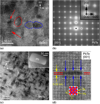
When one PbTe crystal grain was perfectly oriented with its zone axis [001] parallel to TEM incident electron beam, lots of nanoscaled disk-like imperfections (cross section) and the disk-induced lobe-like contrast in the crystal lattice were seen. Figure 1(a) showed that all the disk-like defects were strictly lying on (010), (100), and (001) planes. Owing to the distortion of crystal lattice on both sides of the disks, TEM diffraction contrast images can reveal the lattice strain fields by dark lobe-like regions. For example, in Fig. 1(a), one butterfly-like strain field contrast was highlighted by blue dash lines on both sides of the disk. Except for the defect disks lying on (001) planes [pointed by red arrows or indicated by a red dash line in Fig. 1(a) (discussed later)], disk-like imperfections on (010) and (100) planes can result in diffuse diffractions along [020]* and [200]* directions, respectively, which will lead to the diffraction streaks along the two reciprocal vectors, as shown in Fig. 1(b).
Transmission electron microscopy study of imperfections in pure PbTe crystals: (a) Pb-depleted disks on {001} and their lattice strain fields; (b) selected area electron diffraction pattern showing the diffusive streaks along  and
 ; (c) high volume density of disks and a Pb precipitate lying on (001) (inset); and (d) cross-sectional image of a Pb-depleted disk and a [001] project of PbTe unit cells (inset).

Figure 1(c) showed that the disk-induced butterfly-like contrast dominates the whole bright-field image. As pointed out by Williams and Carter,Reference Williams and Carter17 when the defects are small, like those in our case (2–5 nm in diameter and less than 0.5 nm in thickness), the image may be dominated by the strain field contrast. The areal density of the defect disks (around 9 × 1011 cm−2) may be directly obtained from the micrograph at lower magnification, and the disk volume density is estimated to be around 9 × 1017 cm−3 (if the specimen thickness is around 10 nm in this region), which is more than 50 times higher than the reported volume density of similar defects (but never understood as Pb-depleted disks) in Te-rich PbTe bulk crystals grown by the Bridgman technique.Reference Wang, Shi and Zhang10 The high volume density of the Pb-depleted disks is understandable since our sample preparation method by ball milling usually creates more defects in crystals than the Bridgman method. To confirm that the disks and the strain fields are not the unique features of the samples made by ball milling and hot pressing, we also examined the PbTe ingot bought from Alfa Aesar and found the same disks with a volume density close to 6 × 1017cm−3.
As shown between the blue arrows in Fig. 1(d), the cross-sectional image of the disk shows that the defect was caused by the loss of some atoms on the (100) plane since no dramatic change occurred in the basic lattice structure. As a result of the disk-like deficiency of atoms on the (100) plane, some (100) crystal planes close to the defect disk tilt or distort toward the defect center along the blue arrows, which lead to the formation of lattice strain on both sides of the defect disk. Similar strain contrast lobes were reported in Te-rich PbTe bulk crystal, but were thought to be caused by plate-like defects with Te antisite atoms or interstitial Te atoms.Reference Wang, Shi and Zhang10
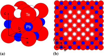
Based on our close TEM examination, we found that the disk-like defects lying on {001} planes (Fig. 1) are Pb-depleted vacancy aggregates, which is supported by the following five reasons. First, as shown in the inset in Fig. 1(c), a pure Pb crystal as precipitate (with estimated volume density of around 3.7 × 1012 cm−3) lying on (001) was identified by TEM and EDS, which implied that the matrix containing the disk-like defects should be Pb deficient, consistent with the existence of the Pb-depleted disks. Second, the spacing between the white spots along [100] or [010] in Fig. 1(d) is 0.32 nm, which is half of the unit cell parameter. In this case, the schematic atomic arrangement in Fig. 1(d) (inset: red and blue spots) showed that each white spot correspondingly represents the atomic column along [001] direction. Therefore, the crystal lattice imperfection between the blue arrows in Fig. 1(d) should be a vacancy aggregation, rather than a precipitate or nanoinclusion, because each of the atomic columns along [001] has been preserved very well without any significant lattice mismatch. Theoretically, as shown in a standard PbTe unit cell in Fig. 2(a), when a disk-like Pb-depleted region [white spots in Fig. 2(b), top view] is formed on (001) plane, the monolayer defect may not destroy the original atom arrangement around the disk and keep all the atomic columns intact along [100] or [010] in TEM examination [Fig. 1(d)]. Third, the diffusion coefficients in the p-type PbTe crystal are  and
 Reference Gomez, Stevenson and Huggins18 which means that the diffusion of Pb atoms is statistically more than 10 times faster than that of the Te atoms. Accordingly, it is reasonable that Pb atoms are much easier than Te to jump out of their original positions and form Frenkel disorder.Reference Gomez, Stevenson and Huggins18, Reference George and Wagner19 The Pb atoms may aggregate due to the metallic bonding and then form Pb precipitates [see the inset in Fig. 1(c)]. The vacancies left by the absence of Pb may coalesce and form the disk-like defects, which has lower energy and are more stable than the individual vacancies. Fourth, it was reported that PbTe crystal was easy to be cleaved along (001) plane,Reference Wang, Shi and Zhang10 implying that the bonding between (001) planes is the weakest. Reasonably, the Pb-depleted disks and Pb precipitates lying on {001} are the ones that lead to the low cleavage energy of PbTe along the {001} planes. Finally, the formation energy of Pb vacancies (0.3 eV) in PbTe crystal is much smaller than that of Te vacancies (1.2 eV),Reference Gomez, Stevenson and Huggins18 which means that Pb vacancies are much easier to form than Te vacancies.
Schematic illustration showing the Pb-depleted disk: (a) PbTe unit cell (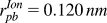 ,
 Reference Wang, Shi and Zhang10) with four Pb atoms removed (in white) and (b) top view of the crystal along [001] with 24 Pb atoms removed (in white) to form a Pb-depleted disk.

Instead of the above five reasons, we could theoretically use Z-contrast scanning TEMReference Pennycook20 to confirm the chemical composition so as to prove the deficiency of Pb around the disk region. However, in practice, it is extremely difficult to obtain such information because the image contrast resulting from some missing atoms is very small and the composition change caused by the missing atoms is an extremely small fraction.
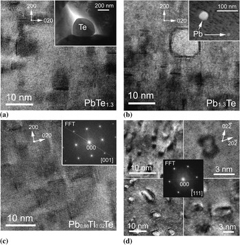
To demonstrate that the Pb-depleted disks are a common feature in PbTe-based alloys, we prepared samples with deeply Pb-deficient and heavily Pb-rich compositions: PbTe1.3 and Pb1.3Te. Figure 3(a) shows that the disk-like Pb vacancies lie on {001} in PbTe1.3 crystal, and the inset shows that the excess Te atoms segregate on the grain boundaries. Even for the heavily Pb-rich Pb1.3Te alloys, Fig. 3(b) shows that Pb vacancies also aggregate on {001} with the excess Pb forming precipitate (shown in the inset). Moreover, our measurement showed that the volume densities of all Pb-depleted disks are around 9 × 1017 cm−3, which are independent of the Pb/Te atomic ratios changing from 1:1.3 to 1.3:1.
Transmission electron micrographs showing (a) the disks and the strain fields in PbTe1.3 with a Te segregate (inset) on grain boundaries; (b) the disks and the strain fields in Pb1.3Te with Pb precipitate (inset) in PbTe crystals; (c) the disks and strain fields in Tl0.02Pb0.98Te with a fast Fourier transform pattern (inset); and (d) four kinds of lattice strain contrasts caused by disks in PbTe along zone axis [111] (top left, deliberately defocused; top right, just focused; bottom left, deviated a little from [111] and defocused; bottom right, deviated a little from [111] and just focused).

To further prove the fact that the Pb depletion is a common feature, we made samples with Tl replacing a small fraction of Pb: Tl0.01Pb0.99Te and Tl0.02Pb0.98Te; these have enhanced Seebeck coefficient due to the creation of impurity band near Fermi level.Reference Heremans, Jovovic, Toberer, Saramat, Kurosaki, Charoenphakdee, Yamanaka and Snyder21 As shown in Fig. 3(c), again, the Pb-depleted disks have also been observed lying on {001} in the samples with a similar volume density. Corresponding to the whole area in Fig. 3(c), the fast Fourier transform pattern (inset) clearly shows that all the spots came from PbTe crystal structure along [001], without any extra spots for precipitates or nanoinclusions, which means the doping atoms Tl have been completely dissolved in the PbTe matrix; the contrast is simply the strain fields rather than precipitates or nanoinclusions.
In TEM observation, lattice strain contrast has been recognized for many years.Reference Williams and Carter17 However, when the defects are very small (less than 10 nm), the related strain contrast images will become difficult to explain due to the lattice distortion around the defect, orientation of the defect in the lattice, orientation of the crystal (specimen) in TEM, and specific TEM operations. Four lattice strain contrast images are presented in Fig. 3(d), which were recorded with PbTe crystal along zone axis [111] (see inset at the center). With this crystal orientation, the angle is 54.7° between [111] and [001] (normal vector of Pb-depleted disk) directions. As shown in Fig. 3(d), all the disks are invisible, but the disk-induced lattice strain fields may generate several kinds of contrast images, which look extremely like “particles” embedded in the matrix. Except for the Pb-depleted disks, we confirm that there is no nanoinclusions or precipitates in the PbTe crystals, which is consistent with a recent publication.Reference He, Gueguen, Sootsman, Zheng, Wu, Zhu, Kanatzidis and Dravid22
For the top view of Pb-depleted disks lying on (001) in the [001] lattice image, as shown in Fig. 1(a), the three disks (two pointed by red arrows and one confined by a red circle) generated different lattice patterns. When the upper crystal slice (on top of the defect) is distorted or rotated a little toward the lower crystal slice (on the bottom of the defect), due to the effect of interference of diffraction electron beams, the Moiré fringe (by two crystals overlapped) can generate several lattice patterns, which are not easy to be interpreted.Reference Muhlberg and Hesse8 In addition, because of the high volume density of Pb-depleted disks, it is plausible that Ag in the Ag-richReference Kanatzidis4 or Ag2Te-richReference Cook, Kramer, Harringa, Han, Chung and Kanatzidis23 or Ag and Sb in the Ag/Sb-richReference Hsu, Loo, Guo, Chen, Dyck, Uher, Hogan, Polychroniadis and Kanatzidis5–Reference Zhou, Li and Kita7 materials may preferentially agglomerate in the Pb-depleted regions in PbTe-based materials to form precipitates or nanoinclusions. So, the Pb-depleted regions are not precipitates or nanoinclusions but the locations where they form.
IV. CONCLUSIONS
In summary, Pb-depleted disks on {001} planes in PbTe, Pb1.3Te, PbTe1.3, Tl0.01Pb0.99Te, and Tl0.02Pb0.98Te crystals are discovered by TEM. These disks are normally 2–5 nm in diameter and less than 0.5 nm in thickness, with a volume density of around 9 × 1017 cm−3. Each of these Pb-depleted disks produces a strong strain field contrast image that looks like a precipitate or nanoinclusion in PbTe-based materials. In some cases when alloying elements are introduced into PbTe crystals, it is possible that some alloying elements preferentially aggregate in the Pb-depleted disk regions and form the so-called nanoinclusions in PbTe matrix. Therefore, we conclude that the image contrasts are not precipitates or nanoinclusions but Pb-depleted disks and strain fields caused by these disks. These disks are probably the locations of the formation of precipitates or nanoinclusions in some of the PbTe-based materials.
ACKNOWLEDGMENTS
The work is funded by the U.S. Department of Energy, Office of Science, Office of Basic Energy Sciences under award no. DE-FG02-08ER46516 (G.C. and Z.F.R.).