Introduction
Materials that are free of imperfections are rare in nature. Defects and impurities both at surfaces and in bulk dictate the properties, limitations, and reliability of materials. Reference Kittel1 Many attempts have been made to exploit defects and maximize their positive impact. One of the earliest approaches was doping, wherein by tuning the impurity concentration, material function was optimized. Reference Koenraad and Flatté2 The chemical approach to material control does have drawbacks, however, due to unintended consequences such as reduced lifetimes, mechanical durability, reliability, and the formation of undesired secondary phases. Lack of local control is another drawback to doping, and preferential modification of confined chemical environments or surfaces is highly desired. Many applications today need functional nanoscale materials, which requires control over defect and dopant distributions with atomic-scale precision. Reference Kalinin, Borisevich and Jesse3
Scanning probe and charged particle microscopes are capable of local tailoring of dopants and defects with high precision. However, the higher throughput of electron- and ion-based microscopes makes these techniques more enticing for localized doping in large-scale applications. Tools like scanning electron microscopy (SEM), scanning transmission electron microscopy (STEM), and focused ion beams (FIBs) are far from new; concepts at the heart of these technologies date back to the 1930s with independent efforts by E. Ruska and M. von Ardenne, which created many flavors of electron microscopy and FIBs today.
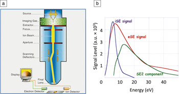
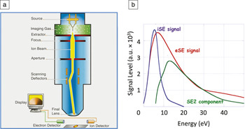
A relatively recent addition to this family is the helium ion microscope (HIM), Reference Notte, Hill, McVey, Farkas, Percival and Ward4 which utilizes a gas field ion source (GFIS) originated by E. Müller in the mid-1950s. Figure 1a shows a cross section of the Carl Zeiss ORION NanoFab—currently the only commercially available HIM—and also able to operate using neon (Ne) ions. The HIM offers high-resolution imaging, large depth of focus, excellent surface sensitivity, high secondary-electron (SE) yield, and several novel contrast mechanisms. Reference Joy5 The technique has shown an unprecedented level of nanoscale control of material properties, thus opening new avenues to materials research. Reference Jesse, Borisevich, Fowlkes, Lupini, Rack, Unocic, Sumpter, Kalinin, Belianinov and Ovchinnikova6
Helium ion microscope (HIM) overview. (a) Simplified cross-sectional diagram of a Zeiss ORION HIM identifying key components. Reference Joy5 (b) Comparison of electron-generated secondary electrons (eSEs) with ion-generated secondary electrons (iSEs), and electron-generated secondary-secondary electrons (SE2) for silicon in the energy range below 50 eV. The eSE signal also contains the SE2 component.
In this article, we present and discuss recent advances in medium-energy ion-beam processing of materials, as well as offer an outlook for future directions in the field. We describe the current state of the He (Ne) ion microscope as a fabrication and engineering tool, and outline new approaches for utilizing ion beams for materials processing and design.
The helium ion microscope
A comprehensive description of HIM technology and applications can be found elsewhere. Reference Hlawacek and Gölzhäuser7 Here, we briefly describe the salient features and underlying principles of the GFIS tool, as well as the fundamentals of ion–surface interactions. The GFIS gun is different from other source technologies such as the liquid-metal ion source (LMIS) for gallium ions, or the thermal-field emitter (Schottky source) and the cold-field emitter (CFE) for electrons. The gas-based ion source available today is an atomically sharp tungsten needle that functions in the 5–50 kV range, at 60–90 K, maintained under ultrahigh vacuum (UHV) conditions of <4 × 10⁻¹⁰ Torr, but operated at 10–7–10–6 Torr of He or Ne gas. Optimized source brightness is typically 5 × 10⁹ A cm–2 sr–1 with a ∼1 eV energy spread. The virtual source size (for He) is <0.25 nm, with total emitted current of ∼150 pA and de Broglie wavelength ∼0.080 pm.
As the ion beam strikes the sample surface, the particles elastically or inelastically scatter. For an elastic process in a two-body system, this interaction can be defined by an interatomic potential, which depends only on the distance between particles. This requires a time-dependent quantum mechanical treatment of the evolution of the electronic systems of the particles as the distance between particles decreases. This becomes increasingly complicated as details of the velocity-dependent excitations of the electronic systems need to be accounted for, necessitating approximations. Reference Lehtinen, Kotakoski, Krasheninnikov and Keinonen8 With inelastic scattering, the electronic systems of the material and the impinging ion can be excited. This can lead to structural changes through electron–phonon coupling and local heating of the target at the impact point, possible destruction of atomic bonds due to formation of an excited state, or ionization. Reference Ziegler9 First-principles calculations offer great insight into details of beam–sample interactions, but can be time consuming and require computational expertise, as well high-performance computing resources. Furthermore, a comprehensive treatment of classical and quantum behavior in ion–sample interaction would need to be taken into account. Notably, efforts are under way for such a combinatorial approach. Reference Garashchuk, Jakowski, Wang and Sumpter10,Reference Ievlev, Jakowski, Burch, Iberi, Hysmith, Joy, Sumpter, Belianinov, Unocic and Ovchinnikova11
In practice, the Monte Carlo (MC) simulation approach allows a rigorous treatment of scattering events, energy distribution of incident ions, recoil target atoms or molecules, and SEs as well as their angular distributions. The results of these simulations are typically easier to acquire, and in the case of freely available packages, do not require extensive expertise. Ziegler et al. Reference Ziegler, Ziegler and Biersack12 developed the SRIM/TRIM simulator, which is the most popular ion–solid interaction simulator to date. Other simulators such as SDTrimSP, MCSIM, and Geant4 are mainly used to calculate ion trajectories and energy loss for energetic ion–solid interactions. Reference Biersack and Eckstein13,Reference Ullrich, Burenkov and Ryssel14 Timilsina et al. recently developed the EnvizION, Reference Timilsina, Tan, Livengood and Rack15 a three-dimensional MC simulator of FIB-induced sputtering. The focus revolves around simulating the topographic evolution of the target material under the ion beam, while taking into account effects such as sputtering, redeposition, and ion-implantation distribution. We expect most readers would be interested in a MC approach as it offers practical answers to common materials-processing questions.
Ion-beam interaction with the sample surface initiates a multistage process that includes many channels of energy dissipation, usually producing SEs. We define SEs as electrons with energy lower than 50 eV. SEs escape from the surface, limited by the work function of the sample, and are subsequently captured by a SE detector, such as that developed by Everhart and Thornley. Reference Everhart and Thornley16 An important distinction between electron-induced and ion-induced SE generation is that ions generate fewer secondary-secondary electrons (SE2) that are a byproduct of excitation by primary SEs traversing the sample. While incident ions yield more SEs per incident ion particle than an incident electron, ions are massive and travel at ≤1% of the velocity of electrons with the same energy, thus producing little ion backscattering and generating fewer SE2s (see Figure 1b). With substantially smaller wavelengths, ions can therefore be expected to outperform electrons in imaging studies. As a result, ion-generated SE images can be expected to have higher resolutions than those generated by electrons due to minimal parasitic contribution from SE2. Ion-beam-generated SE images, therefore, offer better resolutions as well as much enhanced surface detail. Reference Hlawacek, Veligura, van Gastel and Poelsema17
Semiconductor materials processing
Computing power and efficiency owes continuous improvements to the underlying semiconductor processing technology. Successful continuation of Moore’s Law is largely due to a mixed strategy that involves reducing feature size, implementing new architectures, and utilizing novel materials. This multipronged approach has hinged on advancing analytical technologies such as FIB, SEM, and transmission electron microscopy (TEM) that have been at the root of quality assessment and silicon debug since the inception of the semiconductor industry.
Next-generation transistor fin, gate, and interconnect pitch dimensions will have to be scaled ∼70% to transition from the current 14 nm, to the upcoming 10-nm feature spacing. This carries consequences for FIB since positioning precision, material removal, beam damage, and signal-to-noise ratio have to improve in order to provide high-aspect-ratio milled structures. Traditional gallium FIB, while continuously improving, is approaching fundamental limits of sputter yield, SE yield, and contamination. Reference Orloff, Swanson and Utlaut18 Naturally, there are competing technologies such as lithium magneto-optical ionization sources (MOTIS), cesium low-temperature ion sources (LoTIS), multicusp plasma ion sources, and alloy liquid-metal-ion sources, which offer a broad range of ion species as alternative candidates. Reference Hanssen, Hill, Orloff and McClelland19–Reference Bischoff21 To date, the He- and Ne-based Orion NanoFAB is the most promising technology. In this section, we discuss the challenges and opportunities for using GFISs in the semiconductor device industry.
The HIM and a stable GFIS source are relatively new, with the first commercial prototypes emerging in 2006. As this technology matures and expands into other analytical capabilities, it will undoubtedly add value in complex analytical, metrology, and manufacturing problems. In its current state, many of the reported applications have been limited to universities, national laboratories, and semiconductor R&D facilities. Gas-based ion sources are still in their infancy when it comes to large-scale industrial applications, awaiting a breakthrough or a niche application capable of propelling it to mainstream semiconductor application space. Nonetheless, GFIS beams offer unique, sought after attributes in a number of industry areas, including imaging, metrology, and nanomachining.
In the case of the Orion NanoFAB, two separate technological tracks are available, revolving around using He and Ne, respectively. Helium, with a small beam size, lower currents, and excellent stability offers opportunities for higher resolution work; whereas Ne, with higher ion mass and higher current shines in milling—removing material at roughly 50% of the rate of the gallium-based FIBs. Helium-based measurements have demonstrated sub-10-nm resolution imaging on samples prone to charging, such as photomasks and photoresist. Reference Winston, Cord, Ming, Bell, DiNatale, Stern, Vladar, Postek, Mondol and Yang22 Efforts for minimizing the beam size of the Ne beam are also under way. Reference Rahman, McVey, Farkas, Notte, Tan and Livengood23 Robust charge compensation is a clear advantage of ion-based imaging over SEM. Since He ions are positively charged after ionization, charge compensation is relatively straightforward via in situ irradiation of the sample with low-energy electrons. This translates into industry-relevant applications such as mask repair, TEM lamella preparation, and circuit editing.
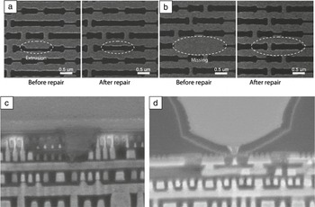
The next generation of mask repair tools, for both optical and extreme ultraviolet (EUV) masks, necessitates improvements in practically every aspect (e.g., higher precision, minimal absorber side etching, limited material layer intermixing, low reflectivity loss, and high etch selectivity). The minimal repairable dimension in the current state-of-the-art electron-beam repair systems is roughly 20–30 nm and selectivity between the two types of phase-shift mask substrates—MoSi and quartz—is not sufficient to avoid overetching at the mask-writing step ( Figure 2a–b). Reference Aramaki, Kozakai, Matsuda, Takaoka, Sugiyama, Oba, Aita and Yasaka24 Gonzales et al. have reported He and Ne etching of nickel top absorber films for EUV lithography mask editing. Reference Gonzalez, Timilsina, Li, Duscher, Rack, Slingenbergh, van Dorp, De Hosson, Klein and Wu25 No discernable nickel etching was observed for room-temperature He exposures at 16 and 30 keV in the dose range of 1 × 10¹⁵–1 × 10¹⁸ ions/cm2; however, TEM revealed subsurface damage to the underlying MoSi multilayer EUV mirror. Stanford et al. demonstrated an in situ infrared pulsed laser approach for He- and Ne-beam-induced damage mitigation, which reduced the implantation and defect concentration by more than 90%. Reference Stanford, Lewis, Iberi, Fowlkes, Tan, Livengood and Rack26 Subsequently, Ne-beam-induced etching at 30 keV was investigated over a similar dose range and was found to successfully remove the entire 50-nm nickel film at a dose of ∼3 × 10¹⁷ ions/cm2.
Mask and device repair. (a) Scanning ion images of holes on a MoSi (HOYA A6L2) mask before and after repair of an extrusion defect and (b) repair of a fully missing feature. Reference Aramaki, Kozakai, Matsuda, Takaoka, Sugiyama, Oba, Aita and Yasaka24 (c–d) Neon (Ne) ion-beam nanomachining of “vias” (through-wafer electrical connections) on 22-nm fin field-effect transistor devices. (c) A 10 kV Ne ion-beam-machined “via” through the transistor region to the signal routing layer. (d) A Ne ion-beam-machined “via” through the silicon substrate, endpointing on a poly (metal-gate) line. Reference Wu, Stern, Ferranti, Xia and Phaneuf27
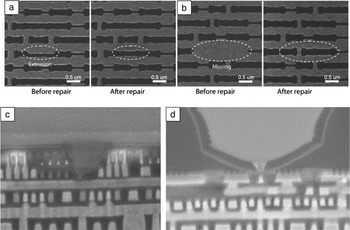
Figure 2c–d illustrates circuit edit of a 22-nm fin field-effect transistor (FinFET) device using a 10 kV Ne ion beam. Reference Wu, Stern, Ferranti, Xia and Phaneuf27 Figure 2c is the result of a process where the target interconnect layers were exposed, followed by ion-beam-induced deposition for the dielectric layer, and finally milling of a narrow “via” (a through-wafer hole for electrical connection) through the dielectric layer to the specific interconnect in order to mimic a chemical-etching process. In Figure 2d, a Ne ion beam was used to edit between the p- and n-doped transistor fins. After successful endpointing on the narrow contact layer and Ga+ ion-beam-induced deposition of the dielectric were completed, the contact layer was re-exposed by Ne ion-beam machining of a 40-nm (full width at half maximum) via. This example highlights Ne’s ability to access a signal at the polygate, source, and drain levels without damaging the device. In this circuit-edit arena, Ne-based milling has demonstrated good nanomachining performance, with 2–3× lower sputter yield and up to 3× higher SE yield relative to Ga+, providing a high level of signal-to-noise ratio and controllability unattainable with Ga+. Reference Hlawacek and Gölzhäuser7 However, undesired side effects of Ne milling such as alteration of material properties, lateral sputtering, and transistor device properties need to be considered in using Ne for large-scale circuit-edit applications. Large interaction volumes limit Ne application in tightly packed areas, and Ne implantation leads to the formation of nanobubbles once the implanted dose exceeds Ne solubility in the substrate. Nonetheless, careful studies have demonstrated Ne viability, with clear advantages over gallium-based sources in a wide variety of circuit-edit applications such as working with interconnects, circuit timing, and fault isolation. Reference Rahman, Notte, Livengood and Tan28 TEM lamella preparation with liftout is essential to many industries. TEM samples are sensitive to damage and Ga+ contaminants, imposing follow-up polishing steps with low-energy Ga+ or Ar+. Wei et al. and Pekin et al. recently demonstrated Ne-based polishing of lamellae preliminarily thinned with a Ga FIB. Reference Wei, Huynh and Ribbe29,Reference Pekin, Allen and Minor30 These results suggest that while Ne ion-beam milling does not significantly reduce the FIB-induced artifacts, the Ne ion beam does enable more precise milling and may be of interest in cases where Ga contamination cannot be tolerated. Furthermore, the reduced Ne sputtering rate of 0.3–0.5 of Ga offers more control during milling; coupled with the current Ne spot size of ∼2 nm in the HIM, this also implies a route for reproducibly making thinner lamellae.
Two-dimensional materials processing
Reproducibly visualizing and modifying materials at the atomic scale is a key first step in fabricating functional nanodevices. HIM images reveal surface topography with a subnanometer-sized beam, as well as allowing material processing via defect engineering at sub-10-nm length scales. Following graphene’s introduction as a unique, high mobility, zero-gap semiconductor, much interest is now aimed at various 2D materials with other functionalities, such as insulators, semiconductors, and correlated electron materials. Transition-metal dichalcogenides (TMDs) and more exotic ferroelectric 2D materials Reference Belianinov, He, Dziaugys, Maksymovych, Eliseev, Borisevich, Morozovska, Banys, Vysochanskii and Kalinin31 offer a breadth of properties to create high-performance transistors Reference Yi, Wu, Liu, Zeng, He and Wang32 and optical devices. Reference Ross, Klement, Jones, Ghimire, Yan, Mandrus, Taniguchi, Watanabe, Kitamura and Yao33 Extensive studies have been conducted to attempt to control properties of 2D nanomaterials by the effects of high-energy ion or electron irradiation. Recently, HIM has focused on “direct-write” manipulation of atomic structures and defects in 2D nanomaterials, pursuing higher resolution and throughput when compared to the focused electron beam. Reference Yoon, Rahnamoun, Swett, Iberi, Cullen, Vlassiouk, Belianinov, Jesse, Sang and Ovchinnikova34
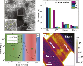
The use of He ion irradiation to establish control over graphene properties has been extensively explored ( Figure 3a–b). Comprehensive Raman studies demonstrate precise control over the defect density by increasing He ion dose and energy, transforming semimetallic graphene to an insulating carbon structure. With an excessive ion dose, a He ion beam can mill out graphene with sub-10-nm resolution owing to its diameter being less than 1 nm; pores as small as 2 nm have been reported. Reference Emmrich, Beyer, Nadzeyka, Bauerdick, Meyer, Kotakoski and Gölzhäuser35 This is relevant to mechanically tailored graphene nanoribbons, whose electronic properties can be changed from semimetallic to semiconducting by atomic-to-nanoscale modification. Defect engineering of graphene has also been utilized to design graphene-based electronic devices, in both a single material system and a stacked van der Waals heterogeneous structure system with other 2D nanomaterials such as hexagonal boron nitride (h-BN). Reference Nanda, Hlawacek, Goswami, Watanabe, Taniguchi and Alkemade36
Two-dimensional materials processing. (a) Aberration-corrected scanning transmission electron microscope images of graphene irradiated at 1017 He+ ions/cm2. Inset is a zoomed-in area highlighted by a white dotted line. (b) Distribution of defect types generated by different irradiating ions. (c) Double log plot of electrical resistivity versus He+ dose for a substrate-supported, mechanically exfoliated bilayer MoS2 flake. Inset: Resistivity measurement as a function of gate bias. (d) Kelvin probe force microscopy image of a WSe2 thin-film transistor with symmetric Ti/Au electrodes in which half of the channel width was exposed with a dose of 5 × 10¹⁴ He+/cm2. Note: MV, monovacancy; STW, Stone–Thrower–Wales defect; S, semiconducting; I, insulating; M, metallic regions. (a–b) Reprinted with permission from Reference Yi, Wu, Liu, Zeng, He and WangReference 32. © 2016 American Chemical Society.
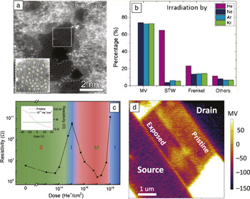
Defects in TMDs can alter the electronic behavior and band structure in a wide variety of ways. Point defects in TMDs can occur intrinsically; however, a variety of methods have been explored for their control. Plasma treatment has the potential to introduce defects as well as to dope TMDs. Reference Azcatl, Qin, Prakash, Zhang, Cheng, Wang, Lu, Kim, Kim and Cho37 Electron-beam irradiation has been used to introduce a variety of point and extended defects. More recently, a focused He ion beam has been used to introduce defects into multilayered MoS2, MoSe2, and WSe2, controllably tuning the materials’ electrical properties from semiconducting to insulating to metallic (Figure 3c–d). Reference Fox, Zhou, Maguire, O’Neill, Ó’Coileáin, Gatensby, Glushenkov, Tao, Duesberg and Shvets38–Reference Iberi, Liang, levlev, Stanford, Lin, Li, Mahjouri-Samani, Jesse, Sumpter, Kalinin and Joy40 Recent work demonstrates that the metallic-like WSe2 and WS2 can be utilized to direct write a logic gate on single TMD flakes and direct-write edge-contacted transistors. These results demonstrate a strategy for generating atomically thin circuitry and show potential for large-scale processing via standard ion implantation. Reference Stanford, Pudasaini, Gallmeier, Cross, Liang, Oyedele, Duscher, Mahjouri-Samani, Wang, Xiao, Geohegan, Belianinov, Sumpter and Rack41
Lin et al. Reference Lin, Carvalho, Kahn, Lv, Rao, Terrones, Pimenta and Terrones42 provide a comprehensive review of defect engineering in TMDs. In addition to graphene and TMDs, other low-dimensional materials, such as copper indium thiophosphate, a 2D van der Waals ferrielectric system, Reference Belianinov, He, Dziaugys, Maksymovych, Eliseev, Borisevich, Morozovska, Banys, Vysochanskii and Kalinin31 show promise in He ion irradiation processing. Local He ion modification can induce ferrielectric switching and improve material conductivity, expanding local control and offering flexibility for designing heterogeneous 2D material devices. Reference Belianinov, Iberi, Tselev, Susner, McGuire, Joy, Jesse, Rondinone, Kalinin and Ovchinnikova43 As exploratory work continues to characterize additional members of this large material library, we expect more properties—and more possibilities to emerge.
FIB-induced deposition
In addition to imaging and milling substrates, the GFIS beam can be utilized to direct-write structures by introducing volatile organometallic or halide gases into the beam path. Reference Silvis-Cividjian and Hagen44 The injected precursors dissociate into etching molecules and attack the surface. This typically requires adding a gas-injection system to the HIM chamber.
At the heart of the process is adsorbate dissociation by the ion beam, as well as contributions by excited surface atoms, and the exiting SEs. The deposition process can be either reaction or mass limited. In the reaction-limited regime, there are more intact precursor molecules than dissociation events. Conversely, in the mass-limited regime, there are more dissociation events than available precursor molecules. This interplay is an important consideration when selecting a beam dwell time at a given pixel, as a reaction-limited regime can quickly transition to a mass-limited regime, and finally, material milling instead of deposition. Reference Silvis-Cividjian and Hagen44
Up to four mechanisms can contribute to the dissociation of the injected precursor (1) surface excitation, (2) thermal spike, (3) SEs, and (4) primary ion beam. Reference Dubner, Wagner, Melngailis and Thompson45,Reference Schmied, Fröch, Orthacker, Hobisch, Trimmel and Plank46 The specific dissociation mechanisms depend on the ion and the material involved in the deposition. It is important to note here that it is the radial distribution of the excited surface atoms, the SEs, and the beam profile that define the lateral resolution of the final deposit. Therefore, pixel dwell and refresh time, to locally recuperate the precursor under the beam, are crucial parameters in the final resolution of deposits.
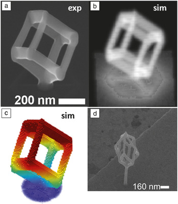
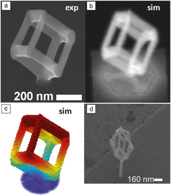
Focused ion-beam-induced deposition (FIBID) with He ions, and focused electron-beam-induced deposition (FEBID) result in comparable metal contents for Me3PtCpMe, WF6, and Co2(CO)8 precursors ( Figure 4 ). Reference Fowlkes, Winkler, Lewis, Stanford, Plank and Rack47 Higher metal content is desirable, as purer metallic interconnects can carry more current and will generally last longer. Composition values from He ion deposition compared to FEBID deposition (He FIBID versus FEBID) are 16–20 at.% versus 13–21 at.% for platinum, and 75–93 at.% versus 85 at.% for tungsten. Reference Wu, Stern, Chen, Huth, Schwalb, Winhold, Porrati, Gonzalez, Timilsina and Rack48–Reference Matsui, Ichihashi and Mito51 This similarity can be attributed to the major role SEs play in precursor dissociation. Silvis-Cividjian and Hagen et al. give an excellent overview of compositions for various precursors with various beams. Reference Lin, Carvalho, Kahn, Lv, Rao, Terrones, Pimenta and Terrones42 Furthermore, He ion and electron deposits from Me3PtCpMe appear similar. The Pt grains embedded in the carbonaceous matrix obtained from He ions are roughly the same size as in FEBID deposits. Reference Alkemade and Miro52 However, Ne ion-beam-induced deposition results in slightly larger grain sizes, approximately 4–5 nm. However, this dissimilarity can be attributed to the initial metal concentration in the precursor, mass- versus reaction-limited regime, or the scan and exposure parameters during deposition.
Focused electron-beam-induced deposition (FEBID) and focused ion-beam-induced deposition (FIBID). (a) Scanning electron microscope (SEM) image of FEBID growth of a cubic frame. The segment length was 200 nm, and the cubic frame was rotated vertically by 54.7°. The rotation made all segment angles equal at 35.3°, requiring a dwell time (τd) of 11.0 ms at a pixel point pitch (Λ) of 1 nm. There were 2008 individual pixel dwells required to write the cubic mesh. (b) Virtual SEM image of the simulation results that mimic the experiment in (a). (c) Simulation result rendered in the form of deposit surface voxels (each volume element is the amount of material at a given dwell time), where the color map is normalized to the vertical z-coordinate. (d) An example of helium FIBID grown deltahedron, a 10-face solid, with a Me3PtCpMe precursor. (a–c) Reprinted with permission from Reference Fowlkes, Winkler, Lewis, Stanford, Plank and RackReference 47. © 2016 American Chemical Society.
Conclusions
The transition from observing bright spots on the phosphor-coated bottom of an Erlenmeyer flask, in the early versions of the field ion microscope built in E. Müller’s lab in 1955, to a commercialized tool today, more than 60 years later, was enabled by critical technologies such as cryogenics, ultrahigh vacuum, gas purification, vibration control, ion optics, and detectors. Although it is clear much development and fundamental research still lies ahead, it is evident that ion beams and gas field ion sources are no longer a restricted novelty, but rather an emerging player in areas of high-resolution imaging, nanofabrication, and direct write. We expect this technology to have a significant impact in physical and biological sciences over the coming years. Specifically, once reliable operation can be guaranteed at beam energies above 100 kV, He and Ne ion microscopy will ultimately be capable of demonstrating atomic-level resolution even on bulk materials.
Furthermore, ongoing efforts in emerging applications, omitted from this perspective, in areas of chemical imaging with secondary ion mass spectrometry and backscattered ions, in situ direct-write with liquids (using specialized enclosed cells, or low-vapor-pressure liquids), and transmission-mode imaging are already under way. Associated density functional theory, Bohmian dynamics, MC, and FIBID specific theory efforts are also picking up pace as additional HIM tools become available.
Finally, atomic-scale manipulation and control in emerging materials are seen as an enabling technology for semiconductors, energy-related applications, and industrial material processing. As efforts in bringing new materials and devices online continue, analytical methods capable of characterization and mass production must keep pace. We believe ion microscopy offers the desired capabilities as well as potentially new ones as the technology evolves.
Acknowledgments
M.J.B., S.K., and O.O. acknowledge research conducted at the Center for Nanophase Materials Sciences, a DOE Office of Science User Facility. A.B. acknowledges research by the Laboratory of Directed Research and Development Program of Oak Ridge National Laboratory, managed by UT-Battelle, LLC, for the US Department of Energy.

Alex Belianinov is a R&D staff member in the Nanofabrication Research Laboratory group at the Center for Nanophase Materials Sciences (CNMS) at Oak Ridge National Laboratory (ORNL). He joined ORNL in 2012 as a postdoctoral fellow in the Scanning Probe Microscopy Group at CNMS. He received his bachelor’s degree in chemistry at Case Western Reserve University in 2007, and his doctorate in analytical chemistry at Iowa State University/Ames Laboratory in 2012. He has co-authored more than 70 articles and book chapters and holds one patent. He received a R&D 100 Award as well as a Microscopy Today Innovation Award in 2016. His current research interests include novel characterization schemes in microscopy, machine learning, and high-performance computing for materials science. Belianinov can be reached by email at belianinova@ornl.gov.

Matthew J. Burch is a postdoctoral research associate at the Center for Nanophase Materials Sciences at Oak Ridge National Laboratory. He received his PhD degree in materials science and engineering from North Carolina State University in 2016. His current research focuses on understanding the connection between materials functionality and its nanoscale chemical and physical structure through electron- and ion-based microscopy. Burch can be reached by email at burchmj@ornl.gov.

Songkil Kim is a postdoctoral researcher at the Center for Nanophase Materials Sciences at Oak Ridge National Laboratory. He received his MS degrees in mechanical engineering at Pusan National University, South Korea, in 2007 and 2009; and his PhD degree in mechanical engineering at the Georgia Institute of Technology in 2014. His current research interests include electron-/ion-beam-based nanofabrication of low-dimensional nanomaterials and nanoelectronic devices and three-dimensional nanostructures. Kim can be reached by email at kims2@ornl.gov.

Shida Tan is a principal engineer in the Platform Engineering Group at Intel Corporation, where she leads R&D projects to develop advanced physical debug technologies for on-die circuit analysis for Intel’s 10 nm/7 nm process technologies. She joined Intel in 2002, after receiving her PhD degree in materials science from Auburn University. She has co-authored more than 80 articles and book chapters, and holds eight issued patents (plus several pending), and three Intel trade secrets. She also holds the position of vice president of the International Society of Electron, Photon, Ion Beam Technology and Nanofabrication. Tan can be reached by email at shida.tan@intel.com.

Gregor Hlawacek is a senior scientist at the Ion Beam Center of the Institute of Ion Beam Physics and Materials Research at Helmholtz-Zentrum Dresden-Rossendorf, Germany. He received his PhD degree in 2007 from the University of Leoben, Austria. He has worked with gas field ion source (GFIS)-based focused ion beam systems since 2009. He has been responsible for GFIS-related projects at the University of Twente, The Netherlands, and since 2014, at the Ion Beam Center. He has been responsible for the introduction of several analytic techniques to the helium (He) ion microscope, including ionoluminescence, channeling-based crystallography, time-of-flight-based backscattering spectrometry as well as time-of-flight-based secondary ion mass spectrometry. He holds one patent, has co-authored more than 60 papers, eight book chapters, and is one of the editors of the first book on He ion microscopy. He received the AT&S Prize from the Austrian Physical Society for the best solid-state PhD thesis in 2008. Hlawacek can be reached by email at g.hlawacek@hzdr.de.

Olga Ovchinnikova is a chemical imaging team lead and research staff scientist in the Nanofabrication Research Laboratory at the Center for Nanophase Materials Sciences at Oak Ridge National Laboratory (ORNL). She received her PhD degree in 2011 from The University of Tennessee, Knoxville, in chemical physics. She was a postdoctoral associate and research staff scientist in the Organic and Biological Mass Spectrometry Group in the Chemical Sciences Division at ORNL. Her research focuses on the relationships between physical structure and chemical functionality at the nanoscale through the development of multimodal imaging platforms, and co-registration of multidimensional data. Ovchinnikova can be reached by email at ovchinnikovo@ornl.gov.