Plasmonic effects on exciton recombination: Enhancing the radiative rate
Modification of the spontaneous emission rate of a single quantum emitter is often credited to Purcell, who in 1946 stated that a resonant electrical circuit could enhance the spontaneous decay of magnetic dipole moments by a factor of 3Qλ3/4π2 V, where Q denotes the quality factor of the circuit, V represents the mode volume, and λ is the wavelength of the emitted radiation. In the past three decades, various microcavities have been realized in the optical domain with the aim of maximizing the Q/V ratio and thus, the Purcell effect on optical transitions, Reference Vahala1 whereby enhancements of a few tens in the Purcell factor have been demonstrated. Reference Press, Götzinger, Reitzenstein, Hofmann, Löffler, Kamp, Forchel and Yamamoto2,Reference Gerard and Gayral3 In addition to modifying the natural photophysics of an emitter, a large Purcell factor also makes it possible to extract more photons from a quantum emitter per unit time.
Although great progress has been made with microcavities, some limitations remain that cannot be easily overcome. One important restriction is that, despite their seemingly small character, microcavities are relatively large. From a fundamental aspect, a microcavity cannot become arbitrarily small, beyond λ/2, where the first resonance takes place. From a practical point of view, the device is even larger because of the finite size of the mirrors and boundaries required for high reflectivity and low diffraction losses. Another difficulty of working with high-Q microcavities is the extreme spectral selectivity, which makes them sensitive to vibrations and temperature drift. Furthermore, it is usually a fabrication challenge to meet the resonance of a particular single emitter. Reference Hennessy, Badolato, Tamboli, Petroff, Hu, Atatüre, Dreiser and Imamoglu4
An attractive alternative approach for enhancing the radiative decay of quantum emitters is to use plasmonic nanoantennas. Reference Sandoghdar, Agio, Chen, Götzinger, Lee, Agio and Alu5 Here, a metallic nanostructure, usually made of gold or silver, increases the local density of states in its near field. In an equivalent picture, the plasmon oscillation inside the metallic particle couples to the dipolar transition of the emitter in a near-field interaction, whereby the coupled system acquires a giant dipole moment, which can interact with the propagating light fields more efficiently. Thus, the metallic nanostructure can act as a receiving and sending subwavelength antenna that enhances the absorption and emission of an emitter. The antenna enhancement depends very sensitively not only on the distance to the emitter, but also on the orientation of its dipole moment. Because the plasmon resonance is usually several tens of nanometers wide, the antenna offers broadband operation in addition to having an ultrasmall footprint. However, the enhancement of the spontaneous emission by plasmonic antennas comes at the cost of quenching caused by nonradiative dissipation channels that open (as a result of metal ohmic losses) in the near field of real metals. In most cases, this quenching process begins to dominate at smaller emitter distances, where high radiative enhancement effects are predicted.
To meet the challenge for precise nanoscale arrangement of emitter and plasmonic nanoantenna, synthesis and assembly methods continue to evolve in accuracy and reproducibility. We review here some of the many strategies being developed for “soft” chemical approaches to precision integration and assembly. We also discuss investigations of the Purcell effect, emitter–emitter coupling, and higher-order emission processes that have been most deeply explored using individual-emitter– (or several-emitter–) nanoantenna pairs fabricated using traditional lithographic methods and/or dynamically and controllably manipulated using scanning probe methods. Importantly, these results, along with theoretical analyses, inspire and motivate continued advancements in large-scale synthesis and assembly.
Toward functional semiconductor and plasmonic nanostructure composites
Nanoparticle self-assembly has been reviewed previously, including self-assembly directly from solution and self-assembly mediated by templates, interfaces, applied fields (electric, magnetic), mechanical shear forces, and light. Reference Grzelczak, Vermant, Furst and Liz-Marzan6–Reference Wang, Xu, Kuang, Xu and Kotov10 Here, we emphasize assembly approaches that have been used to create nanosemiconductor–nanometal hybrids and, in particular, those that have afforded specific plasmonic effects on excitonic properties. Reference Wang, Xu, Kuang, Xu and Kotov10,Reference Banin, Ben-Shahar and Vinokurov11 In general, the semiconductor component of interest is the colloidal quantum dot (QD), but occasionally, we include for completeness additional solution-synthesized quantum emitters, such as semiconductor nanowires and “quantum shells.” The plasmonic nanostructures encompassed by this review are typically metal nanocrystals (NCs) (e.g., gold [Au], silver [Ag]), but complementary to the semiconductor quantum-shell systems, the plasmonic component is occasionally represented by a chemically synthesized metal shell. In Figures 1 and 2 , we summarize various hybrid structures accessed to date through synthesis and soft-assembly approaches.
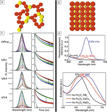
Extended hybrid structures. (a) Schematic of a random-network hybrid assembly of semiconductor nanoemitters (red) and plasmonic nanometals (yellow). (b) Schematic of a binary nanocrystal superlattice (NCSL) comprising quantum dots (QDs; red) and metal nanocrystals (NCs; yellow). (c) Evolution of photoluminescence (PL) and time-resolved PL of CdTe QDs and mixed CdTe QDs-Au NCs during gelation by Cd2+ ions. (Ratios at left are initial CdTe/gold weight ratios, with arrows indicating increasing Cd2+ concentration.) Reference Lesnyak, Wolf, Dubavik, Borchardt, Voitekhovich, Gaponik, Kaskel and Eychmuller19 Au simultaneously quenches and enhances PL, and acts as a FRET spacer. (d) (Top) PL spectra of a close-packed CdSe QD superlattice (blue curve) and a binary NCSL of CdSe QDs and Au NCs (red curves). PL was largely quenched and PL lifetimes were shortened in the case of the binary NCSL compared to the QD-only NCSL. Reference Shevchenko, Ringler, Schwemer, Talapin, Klar, Rogach, Feldmann and Alivisatos32 (Bottom) NCSL-tunable extinction spectra taken from a single domain of binary NCSLs (BNSL) comprising 9.7-nm Au NCs and 17.1-nm Fe3O4 NCs and prepared using different ratios of the two NCs. (c) Adapted with permission from Reference 19. © 2011 American Chemical Society. (d) Adapted with permission from Reference 32 (top). © 2008 American Chemical Society, and adapted with permission from Reference 36 (bottom). © 2013 American Chemical Society.

Extended hybrid structures by self-assembly and in matrixes:
Disordered to ordered
Random networks of interconnected QDs, noble-metal NCs, and QD–NC mixtures can be assembled as highly porous three-dimensional aerogel monoliths or dense two-dimensional xerogel thin films (Figure 1a and 1c). Reference Gacoin, Lahlil, Larregaray and Boilot12–Reference Korala, Li and Brock22 Controlled destabilization of presynthesized QD–NCs, by, for example, chemical or photochemical oxidation of the ligand stabilizers on the QD and/or NC surfaces, removal of surface ligands, or modification of electrostatic stabilization factors, causes QD–NCs to condense into gels. Gels are then dried of interstitial solvent supercritically to form ultralow-density aerogels or under ambient conditions to form less-porous xerogels. Reference Gaponik, Herrmann and Eychmuller15 In general, nanoscale (e.g., quantum) properties are retained, whereas the direct particle–particle connections formed during condensation afford enhanced collective optical and electrical properties, such as enhanced electrical conductivity, increased QD–QD Dexter energy transfer (active at short distances, <2 nm) and Förster resonance energy transfer (FRET; active at longer distances, ∼2–10 nm), metal-induced quenching (by FRET or charge transfer), or plasmon-enhanced QD photoluminescence (PL), and the resultant shortening of nonradiative or radiative lifetimes. Reference Gill and Hope-Weeks17,Reference Lesnyak, Wolf, Dubavik, Borchardt, Voitekhovich, Gaponik, Kaskel and Eychmuller19–Reference Hendel, Lesnyak, Kuhn, Herrmann, Bigall, Borchardt, Kaskel, Gaponik and Eychmuller21 Currently, in the case of mixed QD–NC aerogels, all of these processes could be active. Therefore, a key challenge in this field is to optimize the network structure to favor a targeted outcome, such as PL enhancement, by incorporating appropriate dielectric “spacers” to tune exciton–plasmon interactions for controlled semiconductor–metal spacing. Reference Lesnyak, Wolf, Dubavik, Borchardt, Voitekhovich, Gaponik, Kaskel and Eychmuller19
Nanoparticle colloids with carefully controlled size, shape, and surface properties can self-assemble into a wide array of ordered two- and three-dimensional nanocrystal superlattices (NCSLs) that mimic atomic lattices, and these can be single-component, binary, or ternary NCSLs (Figure 1b and 1d). Reference Dong, Ye, Chen and Murray23–Reference Zeng, Li, Liu, Wang and Sun35 In the absence of significant Coulombic or van der Waals particle–particle interactions or strong ligand–ligand interactions, entropic contributions dominate, such that the nanoparticle colloids behave as “hard spheres” and pack in various high-density configurations, depending on the ratio of the radii of the constituents. Interparticle interactions play a significant role in the assembly of semiconductor/metal NCs, as a result of strong metal–metal van der Waals interactions, which favor close metal–metal associations. Reference Bodnarchuk, Kovalenko, Heiss and Talapin29
Of the highly ordered NCSLs comprising more than one component, >20 binary NCSLs, Reference Shevchenko, Talapin, Murray and O’Brien26,Reference Chen, Ye, Oh, Kikkawa, Kagan and Murray28 and only a few ternary NCSLs, Reference Dong, Ye, Chen and Murray23,Reference Evers, Friedrich, Filion, Dijkstra and Vanmaekelbergh24,Reference Paik, Diroll, Kagan and Murray27 are known to date. These have been constructed from two metals, two or three semiconductors, two or three magnetic nanoparticles, or combinations thereof. Despite the structural diversity and sophistication, efforts to exploit new functionality resulting from ordered arrays of dissimilar but interacting nanoparticles remain limited to exchange-coupling and dipolar interactions in assemblies of magnetic nanoparticle pairs, Reference Chen, Ye, Oh, Kikkawa, Kagan and Murray28,Reference Chen, Dong, Cai, Ye, Kang, Kikkawa and Murray30,Reference Dong, Chen, Ye, Kikkawa and Murray31,Reference Zeng, Li, Liu, Wang and Sun35 enhanced electronic conductivity in semiconductor mixtures, Reference Urban, Talapin, Shevchenko, Kagan and Murray34 tunable plasmonic properties (e.g., strength of near-field couplings), Reference Ye, Chen, Diroll and Murray36 structure-correlated catalytic activity, Reference Kang, Ye, Chen, Qi, Diaz, Doan-Nguyen, Xing, Kagan, Li, Gorte, Stach and Murray37 and fluorescence quenching in the case of metal–semiconductor pairing. Reference Shevchenko, Ringler, Schwemer, Talapin, Klar, Rogach, Feldmann and Alivisatos32 The last of these involved self-assembly of CdSe QDs and Au NCs, and fluorescence spectroscopy studies revealed PL quenching and shortening of QD PL lifetimes. Thus, as for the disordered-network assemblies described earlier, optimization of exciton–plasmon interactions in semiconductor–metal multicomponent NCSLs through nanoscale positioning and spacing will require the inclusion, for example, of nanospacers. Reference Tripathi, Praveena and Basu38–Reference Zhang, Marocico, Lunz, Gerard, Gun’ko, Lesnyak, Gaponik, Susha, Rogach and Bradley40
Hybrid excitonic–plasmonic pairs in single nanostructures:
Direct synthesis and molecular linkers
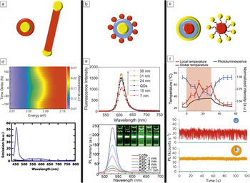
Single nanoconstructs exhibiting uninterrupted semiconductor–metal connections can be directly synthesized (Figure 2a and 2d). Results from this approach have been reviewed previously, Reference Banin, Ben-Shahar and Vinokurov11 with examples ranging from symmetrical metal-core–semiconductor-shell nanostructures Reference Guardia, Korobchevskaya, Casu, Genovese, Manna and Comin41,Reference Zhang, Tang, Lee and Ouyang42 to anisotropic “nanodumbbells” Reference Costi, Cohen, Salant, Rabani and Banin43 and metal-tipped tetrapods. Reference Mokari, Rothenberg, Popov, Costi and Banin44,Reference Mishra, Lian, Chakrabortty, Lin and Chan45 Structures comprising direct semiconductor–metal interfaces have been used to demonstrate plasmonics-enhanced nanoscale light–matter and light–matter–spin interactions; for example, a resonantly coupled (metal local surface-plasmon resonance [LSPR] overlapping with emitter first-exciton energy) gold core and CdSe shell afforded an enhanced optical Stark effect and ultrafast coherent spin manipulation. Reference Zhang, Tang, Lee and Ouyang42 More commonly, semiconductor–metal nanoscale heterostructures have been studied in the context of light-induced charge separation and resulting applications in photocatalysis, Reference Banin, Ben-Shahar and Vinokurov11 where this very feature—rapid charge transfer from semiconductor to metal—results in fluorescence quenching, such as in the case of metal- (gold-, silver-) tipped semiconductor (CdSe, CdS, ZnO) nanorods, Reference Mokari, Rothenberg, Popov, Costi and Banin44,Reference Saunders, Popov and Banin46,Reference Pacholski, Kornowski and Weller47 and Au2Cd alloy-core–CdSe-shell NCs. Reference Guardia, Korobchevskaya, Casu, Genovese, Manna and Comin41
Spatially limited hybrid nanoconstructs. (a) Schematic depicting semiconductor nanoemitter (e.g., shell, rod) (red) and metal plasmonic nanocrystal (NC) (yellow) single nanostructures containing direct semiconductor–metal interfaces. (b) Schematic of a metal-planet–quantum dot (QD)-satellite nanostructure, wherein the two components are separated by a spacer (e.g., SiO2, polymer, DNA). (c) Schematics of QD-core–metal-shell and QD-planet–metal-satellite nanostructures, wherein the two components are separated by a spacer (e.g., SiO2, polyelectrolyte layers, DNA). (d) (Top) Optical Stark effect (OSE): Time-resolved linear optical absorption spectra with subresonant excitation energy (1.892 eV at 1.45 GW cm−2), where the subresonant and probe laser beams are co-polarized. (Bottom) Complete quenching of the photoluminescence (PL) of CdS nanorods (dotted line) upon growth of gold tips (solid line). (e) (Top) PL spectra of CdSe/ZnS QDs and hybrid silver/SiO2/QDs as a function of the SiO2 spacer thickness. (Bottom) PL spectra of bare CdTe QDs and gold/SiO2/QDs as a function of spacer thickness. (f) (Top) Multifunctionality afforded by CdSe/CdS giant-QD/SiO2/gold-shell hybrid constructs: Simultaneous excitation of the QD (ultraviolet excitation) and gold-shell (near-infrared excitation) components affords simultaneous optical readout (QD PL), thermometry (QD PL is temperature-sensitive), and photothermal heating (gold shell). (Bottom) PL intensity as a function of time (binning time, 10 ms) for CdSe/CdS QDs (red trace) and QD/SiO2/gold-shell hybrid nanostructures (orange trace), revealing radiative efficiences of neutral and charged states becoming almost equal with Au-shell addition. (d) Adapted with permission from Reference 42 (top). © 2010 Macmillan Publishers Ltd. Nature, and adapted with permission from Reference 46 (bottom). © 2006 American Chemical Society. (e) Adapted with permission from Reference 49 (top). © 2013 American Chemical Society, and adapted with permission from Reference 50 (bottom). © 2013 OSA Publishing. (f) Adapted with permission from Reference 59 (top). © 2015 Royal Society of Chemistry, and adapted with permission from Reference 57 (bottom). © 2015 Macmillan Publishers Ltd: Nature Nanotechnology.

To avoid the quenching observed for direct-junction semiconductor–metal nanoconstructs, dielectric spacers have been synthetically added (Figure 2b and 2e). Reference Liu, Prall and Klimov48–Reference Tang, Xu, Guo, Zhuang, Tian, Wang, Duan and Pan50 Here, the core is a metal nanocrystal (gold Reference Liu, Prall and Klimov48–Reference Tang, Xu, Guo, Zhuang, Tian, Wang, Duan and Pan50 or silver Reference Naiki, Masuhara, Masuo, Onodera, Kasai and Oikawa49 ) overcoated with a thickness-tunable SiO2 layer using a modified Stöber process. Reference Liu, Prall and Klimov48–Reference Liz-Marzan, Giersig and Mulvaney51 The SiO2 surface is subsequently activated for QD (CdSe, Reference Liu, Prall and Klimov48 CdSe/ZnS, Reference Naiki, Masuhara, Masuo, Onodera, Kasai and Oikawa49 CdTe Reference Tang, Xu, Guo, Zhuang, Tian, Wang, Duan and Pan50 ) binding by the addition of aminosilane coupling agents, Reference Liu, Prall and Klimov48–Reference Tang, Xu, Guo, Zhuang, Tian, Wang, Duan and Pan50 giving a “planet–satellite” configuration. The added control afforded by this synthesis over semiconductor–metal spacing has yielded tunable effects ranging from nonradiative damping (quenching) to field-enhanced PL (either excitation Reference Naiki, Masuhara, Masuo, Onodera, Kasai and Oikawa49 or emission Reference Tang, Xu, Guo, Zhuang, Tian, Wang, Duan and Pan50 enhancement) as a function of SiO2 thickness. Both quenching and enhancement have been realized for similar constructs in which the SiO2 layer is effectively replaced by molecular spacers or rigid DNA linkers. Reference Lee, Govorov and Kotov52–Reference Sun, Tian, Zhang, Xu, Sfeir, Cotlet and Gang56 For example, Lee et al. demonstrated a “nanoscale thermometer” using a poly(ethylene glycol) (PEG) spacer, where PEG’s responsiveness to heat (thermal swelling) afforded QD PL intensity tuning through dynamic control of the CdTe QD–Au distance. For this case of overlapping PL and LSPR energies, PL enhancement occurred at the shortest distances. Reference Lee, Govorov and Kotov52 In contrast, in QD–Au constructs connected by rigid DNA linkers, QD PL was quenched with a distance dependence characteristic of FRET (1/d Reference Grzelczak, Vermant, Furst and Liz-Marzan6 dependence, where d is the distance), Reference Gueroui and Libchaber53 or of either FRET or a nanometal surface energy transfer mechanism (1/d Reference Hennessy, Badolato, Tamboli, Petroff, Hu, Atatüre, Dreiser and Imamoglu4 dependence), depending on the Au NC size and the extent of PL–LSPR overlap. Reference Li, Cushing, Wang, Shi, Hornak, Hong and Wu55
In an inverse scenario compared to these metal-core–semiconductor-shell nanostructures, metal shells have been grown or assembled around semiconductor cores (Figure 2c and 2f). Reference Ji, Giovanelli, Habert, Spinicelli, Nasilowski, Xu, Lequeux, Hugonin, Marquier, Greffet and Dubertret57–Reference Karan, Keller, Sampat, Roslyak, Arefin, Hanson, Casson, Desireddy, Ghosh, Piryatinski, Iyer, Htoon, Malko and Hollingsworth59 Here, rather than quantum semiconductor shells serving the role of the emitter, more traditional and potentially better performing colloidal QDs comprise the emitter, whereas the gold shell imparts multifunctionality (combined QD PL and gold scattering or absorption-mediated photothermal heating) Reference Jin and Gao58,Reference Karan, Keller, Sampat, Roslyak, Arefin, Hanson, Casson, Desireddy, Ghosh, Piryatinski, Iyer, Htoon, Malko and Hollingsworth59 or Purcell effects. Reference Ji, Giovanelli, Habert, Spinicelli, Nasilowski, Xu, Lequeux, Hugonin, Marquier, Greffet and Dubertret57
Jin and Gao reported a novel approach for gold-shell synthesis that used a peptide “gold deposition template,” circumventing the need for presynthesized gold nanoclusters as structural templates and affording a new opportunity for growing ultrathin shells (<5 nm58 versus 5–20 nm60,61). In addition, by adding one to two polyelectrolyte-bilayer spacers, they decreased the QD PL quenching compared to that of direct-contact hybrid structures (45–75% versus ∼100% quenching). Following a similar approach, but modifying and elucidating the highly pH-dependent gold-reduction process, Karan et al. employed thicker spacers in the form of SiO2 layers of controlled thickness (10–17.5 nm). Reference Karan, Keller, Sampat, Roslyak, Arefin, Hanson, Casson, Desireddy, Ghosh, Piryatinski, Iyer, Htoon, Malko and Hollingsworth59 They also used thick-shell or “giant” CdSe–CdS core–shell QDs (g-QDs) Reference Chen, Vela, Htoon, Casson, Werder, Bussian, Klimov and Hollingsworth62–Reference Vela, Htoon, Chen, Park, Ghosh, Goodwin, Werner, Wells, Casson and Hollingsworth64 as the emitter, such that the combination of a thicker spacer layer and a more stable QD could afford complete suppression of gold-mediated quenching. Reference Karan, Keller, Sampat, Roslyak, Arefin, Hanson, Casson, Desireddy, Ghosh, Piryatinski, Iyer, Htoon, Malko and Hollingsworth59 In addition, it was demonstrated both experimentally and theoretically that the interplay of the thicknesses of the SiO2 spacer and gold shell allows precise tuning of the LSPR from the visible to the near-infrared range, as well as large gold absorption cross-sections despite a compact total particle size (40–60-nm “inorganic” diameter). Reference Karan, Keller, Sampat, Roslyak, Arefin, Hanson, Casson, Desireddy, Ghosh, Piryatinski, Iyer, Htoon, Malko and Hollingsworth59
In contrast to the thin-gold-shell examples, Ji et al. established a true “plasmonic resonator” effect in the synthetic construction of a QD enveloped in a thick SiO2 shell (35 nm) coated with a thick gold shell (20 nm), which afforded overlap of the QD PL and the gold plasmon resonance peak. Reference Ji, Giovanelli, Habert, Spinicelli, Nasilowski, Xu, Lequeux, Hugonin, Marquier, Greffet and Dubertret57 In this way, they targeted strong QD–Au coupling, which they observed in the form of neutral and charged states having comparable radiative efficiencies resulting from Purcell enhancement of radiative recombination rates compared to nonradiative Auger recombination, similar to effects observed for CdSe–ZnS QDs dispersed on nano-roughened gold films. Reference Shimizu, Woo, Fisher, Eisler and Bawendi65
Finally, it is worth noting that structures comprising single QDs encircled by multiple Au NCs can be synthesized using various modifications of the DNA linker approach Reference Fu, Micheel, Cha, Chang, Yang and Alivisatos66 or, more recently, “DNA origami” scaffolds (Figure 2c). Reference Schreiber, Do, Roller, Zhang, Schuller, Nickels, Feldmann and Liedl67 The latter approach takes advantage of the ability of DNA to self-assemble into designed two- and three-dimensional nanostructures by the interaction between a long DNA “scaffold” strand with many short DNA “staple” strands. Reference Rothemund68–Reference Douglas, Marblestone, Teerapittayanon, Vazquez, Church and Shih70 Adoption of the DNA origami approach to the assembly of nanomaterials, including the creation of semiconductor–metal hybrid nanostructures, affords an important opportunity to tune separation distances from ∼5 to 200 nm in planet–satellite configurations, with possible implications for surface plasmon amplification by stimulated emission of radiation technologies and self-assembled metamaterials. Reference Schreiber, Do, Roller, Zhang, Schuller, Nickels, Feldmann and Liedl67
Experiments and simplified systems to observe effects of hybridization
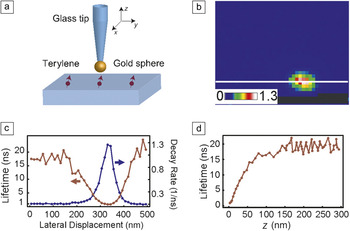
Considering the huge dependence on position and polarization of plasmonic antenna effects, measurements have been conducted on individual emitters coupled to individual nanoantennas to avoid ensemble averaging, with the first experiments reported about 10 years ago. Reference Farahani, Pohl, Eisler and Hecht71–Reference Anger, Bharadwaj and Novotny73 Figure 3a displays a schematic of an experiment in which a single molecule was coupled to a single gold nanosphere attached to the end of a glass fiber tip. The ability to position the antenna with nanometer precision and the use of a system with defined dipole orientation and high photophysical stability Reference Pfab, Zimmermann, Hettich, Gerhardt, Renn and Sandoghdar74 were key to obtaining a more than 20-fold shortening of the fluorescence lifetime accompanied by a similar enhancement in the total emitted photons. Reference Kühn, Håkanson, Rogobete and Sandoghdar72,Reference Kuhn, Mori, Agio and Sandoghdar75,Reference Eghlidi, Lee, Chen, Götzinger and Sandoghdar76 Figure 3b–3d presents data on the enhancement of the spontaneous emission rate of a terylene molecule as a function of its relative lateral position with respect to the nanoantenna.
(a) Schematic of an experiment designed to measure the effects of a nanoantenna on an individual emitter: A single gold nanosphere was attached to the end of a near-field probe and was controllably positioned with respect to a single aligned terylene molecule. (b) Spatial image of the fluorescence decay rate (in units of 1/ns) of a single molecule as a function of nanosphere position. (c) Cross-section depicted in (b) and its inverse, representing the fluorescence lifetime in nanoseconds. (d) Fluorescence lifetime as a function of the axial separation (z) between the antenna and molecule. Adapted with permission from Reference 72. © 2006 American Physical Society.

Although a nanospherical antenna is ideal for controllable and quantitative measurements, it does not offer the highest performance. Indeed, many theoretical Reference Rogobete, Kaminski, Agio and Sandoghdar77–Reference Chen, Agio and Sandoghdar80 and experimental Reference Ji, Giovanelli, Habert, Spinicelli, Nasilowski, Xu, Lequeux, Hugonin, Marquier, Greffet and Dubertret57,Reference Lee, Eghlidi, Chen, Renn, Götzinger and Sandoghdar81–Reference Curto, Volpe, Taminiau, Kreuzer, Quidant and van Hulst83 works have studied structures with alternative shapes and sizes. The key challenge, however, is to design plasmonic nanoantennas that yield a large spontaneous emission enhancement without significant quenching. Here, conical antennas appear to be very promising because they can enhance the radiative rate by several thousand times while keeping the quantum efficiency higher than 70%. Reference Mohammadi, Kaminski, Sandoghdar and Agio79,Reference Schafer, Gollmer, Horrer, Fulmes, Weber-Bargioni, Cabrini, Schuck, Kern and Fleischer84,Reference Chen, Götzinger and Sandoghdar85 As the enhancement effects become larger, a high degree of control over the emitter position and orientation becomes more crucial.
Plasmonic and antenna effects on emission characteristics: Directionality, polarization, collection efficiency
The previous section has shown that even simple antenna geometries allow for very large spontaneous emission enhancements. The high symmetry of these antennas suitable for the enhancement of the spontaneous emission rate does not redistribute the angular emission pattern sufficiently to improve the photon collection efficiency. However, several structures have been devised to achieve a high degree of emission directionality. For example, QDs have been successfully coupled to miniaturized Yagi-Uda antennas. Reference Curto, Volpe, Taminiau, Kreuzer, Quidant and van Hulst83 Furthermore, QDs and color centers have been coupled to plasmonic nanowires that convert the common dipolar emission pattern to guided modes of a subwavelength waveguide. Reference Schell, Kewes, Hanke, Leitenstorfer, Bratschitsch, Benson and Aichele86–Reference Akimov, Mukherjee, Yu, Chang, Zibrov, Hemmer, Park and Lukin88 Unfortunately, the intrinsic losses associated with plasmonic structures prevent very high collection efficiencies. Thus, there exist efforts to replace plasmonic structures with dielectric ones, Reference Yalla, Le Kien, Morinaga and Hakuta89–Reference Lund-Hansen, Stobbe, Julsgaard, Thyrrestrup, Sunner, Kamp, Forchel and Lodahl91 with planar antennas reaching a collection efficiency of 99%. Reference Hennessy, Badolato, Tamboli, Petroff, Hu, Atatüre, Dreiser and Imamoglu4,Reference Lee, Chen, Eghlidi, Kukura, Lettow, Renn, Sandoghdar and Götzinger92,Reference Chu, Brenner, Chen, Ghosh, Hollingsworth, Sandoghdar and Götzinger93 Using such antenna devices could lead to a number of very exciting developments in single-photon technologies, where individual photons could be obtained on demand and with near-unity certainty.
Plasmonic effects on multiexciton processes and photon emission statistics
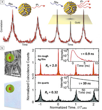
Beyond impacting emitter exciton behavior, interactions with plasmonic nanostructures can modify the radiative and nonradiative recombination processes of multiexciton states. Reference Cheng, Yuan, Wang, Lin, Shen, Hung, Tang and Tseng94–Reference Wang, Karan, Nguyen, Ghosh, Sheehan, Hollingsworth and Htoon107 Normally, because of Auger-mediated processes, multiexciton emission is suppressed, Reference Klimov, Mikhailovsky, McBranch, Leatherdale and Bawendi108 such that a single emitter only produces one photon in a pulsed-excitation cycle. As a result, the second-order photon-correlation function (g (2), which represents the distribution histogram of two successive photon-detection events) acquired under pulsed excitation exhibits little contribution from the zero-time-delay peak, that is, a low probability of detecting two photons during one excitation cycle. This condition is called photon “anti-bunching.” In contrast, recent g (2) studies of QDs coupled to various metal surfaces Reference Cheng, Yuan, Wang, Lin, Shen, Hung, Tang and Tseng94,Reference LeBlanc, McClanahan, Jones and Moyer98,Reference Naiki, Masuo, Machida and Itaya102 and nanostructures Reference Dey, Zhou, Tian, Jenkins, Chen, Zou and Zhao97,Reference Yuan, Wang, Cheng, Wang, Kuo, Shih and Tang103,Reference Park, Ghosh, Xu, Mack, Wang, Hollingsworth and Htoon105,Reference Wang, Karan, Nguyen, Ghosh, Sheehan, Hollingsworth and Htoon107 have revealed dramatic strengthening of the zero-time-delay peak (i.e., photon “bunching”) ( Figure 4 ). At low pump fluence, the area ratio of the center and side peaks of the g (2) function (g (2) (0)/g (2) (T)) reflects the ratio of biexciton to single-exciton quantum yields (Q 2X/Q 1X), Reference Nair, Zhao and Bawendi109,Reference Park, Malko, Vela, Chen, Ghosh, Garcia-Santamaria, Hollingsworth, Klimov and Htoon110 so these results indicate a strong enhancement of biexciton emission efficiency relative to that of single-exciton emission.
(a) CdSe/ZnS quantum dots (QDs) dispersed on a nano-roughened gold surface Reference Liu, Kumar, Hu, Cheng and Irudayaraj100 and (b) CdSe/CdS giant-QDs (g-QDs) dispersed on a silver nanoflake film Reference Chu, Brenner, Chen, Ghosh, Hollingsworth, Sandoghdar and Götzinger93 show strong enhancement in the degree of photon bunching (peak area ratio, g (2) (0)/g (2) (T)), with the center peak increasing to ∼0.5 in the case of standard QDs and exceeding 1 (maximum ∼2.0) in the g-QD example. (a) Adapted with permission from Reference 98. © 2013 American Chemical Society. (b) Adapted with permission from Reference 104. © 2013 American Physical Society.

This enhancement is commonly interpreted as resulting from plasmonic enhancement of bi- and higher-order multiexciton radiative recombination processes. Reference LeBlanc, McClanahan, Jones and Moyer98,Reference Masuo, Naiki, Machida and Itaya101,Reference Naiki, Masuo, Machida and Itaya102 However, the fact that a similar enhancement of Q 2X/Q 1X can also be observed for QDs spread on an indium tin oxide substrate Reference Cheng, Yuan, Wang, Lin, Shen, Hung, Tang and Tseng94 —where no plasmonic enhancement of any radiative recombination process is expected—suggests that apparent plasmonic enhancement of bi-/multiexciton efficiencies can, instead, result simply from a reduction of single-exciton quantum yields (QYs) due to the nonradiative processes discussed previously—direct charge tunneling or FRET to the metal. Thus, these results should be interpreted carefully.
Indeed, Park et al. showed that core/thick-shell or “giant” QDs (g-QDs) coupled to silver “nanoflakes” can exhibit strong photon bunching with the center peak of the g (2) distribution reaching two times the area of the side peaks, which requires that the biexciton QY (Q 2X) exceeds the single-exciton QY (Q 1X) (Figure 4b). Reference Park, Ghosh, Chen, Piryatinski, Xu, Mack, Wang, Klimov, Hollingsworth and Htoon104,Reference Park, Ghosh, Xu, Mack, Wang, Hollingsworth and Htoon105 This condition cannot arise from simple enhancement of biexciton radiative decay rate alone but requires an overall “quenching” (g-QD/metal PL ∼1/10th g-QD PL).
Plasmon-assisted coupling between individual emitters
In addition to enhancing the radiative recombination rate of a quantum emitter, polarization of a metal nanostructure can result in near-field electric interactions that are known to induce coupling between nearby nanoemitters. As such, plasmonics is a potentially powerful tool for enhancing FRET-based energy funneling in the context of photovoltaic and sensing applications and for inducing entanglement between the quantum states of two or more nanoemitters for a wide variety of optical-communication and quantum-information technologies.
Provided that donor and acceptor emitters are located in close proximity to a metal NC, the energy transfer facilitated by the surface plasmon modes can be interpreted semiclassically. The electric field associated with the transition dipoles of the donor and acceptor emitters (i.e., QDs) polarizes the metal NC, creating oscillating images. The near-field interactions between the donor and acceptor dipole images open an additional pathway for energy flow. This pathway—because of the strong polarization of the metal NC—can dominate the total energy-transfer rate, significantly increasing the rate values. Reference Durach, Rusina, Klimov and Stockman111 Details on the interplay between different plasmon-assisted pathways to the total FRET rate have been previously considered. Reference Pustovit and Shahbazyan112,Reference Govorov, Bryant, Zhang, Skeini, Lee, Kotov, Slocik and Naik113
Experimentally, plasmonic enhancement of FRET between different types of donor–acceptor pairs was demonstrated in recent ensemble-level studies. Reference Zhang, Marocico, Lunz, Gerard, Gun’ko, Lesnyak, Gaponik, Susha, Rogach and Bradley40,Reference Zhou, Li, Yang, Peng, Su, Zhang, Li, Kim, Yu, Zhou, Hao and Wang114,Reference Wu and Wang116 In particular, by systematically analyzing PL decay rates, emission spectra, and intensities of layered structures comprising Au NCs, acceptor–donor QD layers, and spacer layers, Ozel et al. demonstrated the ability to enable/disable coupled plasmon–exciton formation selectively at the donor or acceptor site of their choice. Reference Ozel, Hernandez-Martinez, Mutlugun, Akin, Nizamoglu, Ozel, Zhang, Xiong and Demir115
Furthermore, using a similar acceptor-QD/metal/donor-QD three-layer structure with varying spacer-layer thicknesses, Zhang et al. investigated the distance dependence of the local-surface-plasmon-coupled FRET process. Reference Zhang, Marocico, Lunz, Gerard, Gun’ko, Lesnyak, Gaponik, Susha, Rogach and Bradley40 Their analysis revealed that the Förster radius defining the range of FRET processes is increased from 4.2 nm for typical donor–acceptor pairs to values exceeding 10 nm for plasmon-coupled FRET.
Whereas FRET coupling between ensembles of donor and acceptor QDs can be utilized as an effective exciton-transport mechanism in light-harvesting and -sensing applications, the coupling of a few individual QDs into “molecule-like” quantum states might afford important building blocks for solid-state quantum computation architecture Reference Wu and Wang116–Reference Stinaff, Scheibner, Bracker, Ponomarev, Korenev, Ware, Doty, Reinecke and Gammon119 and many quantum-photonic–plasmonic devices such as single-photon transistors Reference Neumeier, Leib and Hartmann120,Reference Chang, Sorensen, Demler and Lukin121 and routers Reference Hoi, Wilson, Johansson, Palomaki, Peropadre and Delsing122 that are needed for realization of quantum-communication networks.
Along these lines, recent theoretical studies have shown that plasmon-coupled FRET can also induce strong coupling and even entanglement between multiple QDs coupled to a plasmonic structure. Reference Martin-Cano, Martín-Moreno, García-Vidal and Moreno123 One of the goals in employing surface plasmon modes is to achieve an entanglement of excitonic qubits at distances exceeding the operating wavelength, requiring the use of plasmonic waveguide structures capable of supporting long-range plasmon–polariton modes.
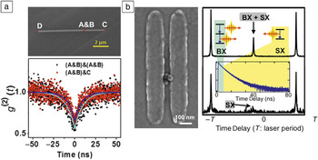
In the laboratory, QDs (and other quantum emitters) have been coupled to silver nanowires, and exciton–plasmon–photon conversion has been demonstrated, Reference Heeres, Kouwenhoven and Zwiller124 as well as single-plasmon generation, routing, and detection. Reference Li, Wei and Xu125 Coupling of multiple QDs to a silver nanowire through “by-chance” deposition was also recently shown. Reference Kolesov, Grotz, Balasubramanian, Stoehr, Nicolet, Hemmer, Jelezko and Wrachtrup126 Similar to previous studies, Reference Kolesov, Grotz, Balasubramanian, Stoehr, Nicolet, Hemmer, Jelezko and Wrachtrup126,Reference Gonzalez-Tudela, Martin-Cano, Moreno, Martin-Moreno, Tejedor and Garcia-Vidal127 in this case, it was demonstrated that single photons emitted by individual quantum emitters are converted into plasmons that propagate along the length of the metal nanowire and are then converted back into single photons. By performing g (2) measurements, the researchers found that two QDs spaced sufficiently close to be excited simultaneously (∼200 nm) exhibited photon statistics characteristic of two independent emitters (g (2) (T =0) ≈ 0.5) ( Figure 5a). Reference Kolesov, Grotz, Balasubramanian, Stoehr, Nicolet, Hemmer, Jelezko and Wrachtrup126 In contrast, Wang et al. recently demonstrated that small clusters of two to three SiO2-coated g-QDs coupled to a plasmonic (gold) gap-bar antenna can exhibit complete photon antibunching—a characteristic of single quantum emitters, despite multiple optically active g-QDs being present (Figure 5b). Reference Wang, Karan, Nguyen, Ghosh, Sheehan, Hollingsworth and Htoon128 Through a detailed analysis of their emission characteristics, they further showed that the observed photon antibunching resulted from plasmonics-enhanced dipole–dipole interactions (i.e., metal-induced formation of a coupled QD–QD emissive state). In this case, the presence of the SiO2 shell yielded a QD–QD separation distance of at least 30 nm, rendering alternative interpretations of the data, such as conventional dipole–dipole interaction, not physically possible. Furthermore, they additionally concluded that the observed complete antibunching behavior resulted not from the existence of nonemissive QDs in the clusters but from the formation of novel coupled-QD “molecules,” an important step toward entangled-photon generation.
(a) (Top) Scanning electron microscope (SEM) image of two quantum dots (QDs) (labeled A and B) coupled to a silver nanowire (C to D) with a separation of less than 200 nm afford (bottom) a trace of the second-order photon-correlation function (g (2)(t)) characteristic of two independent QDs. (b) (Left) SEM image of three SiO2-coated giant-QDs positioned within the gap of a gold gap-bar antenna exhibit (bottom right) nearly complete photon antibunching in the single-exciton (SX) g (2) trace, which was reconstructed from the (top right) raw g (2) trace by rejecting photons of the biexciton (BX) emission process that arrive at early time delays. (a) Adapted with permission from Reference 125. © 2014 American Chemical Society. (b) Adapted with permission from Reference 128. © 2015 John Wiley and Sons.

Conclusions and outlook
Whether through conventional lithography, scanning probe techniques, or “soft” chemical synthesis and assembly approaches, an important emerging aim of creating hybrid semiconductor–metal (excitonic–plasmonic) couples is to realize enhanced or even new functionality that is unachievable by individual systems. Furthermore, although the intention is generally to suppress competitive ohmic losses, occasionally, enhancement of this effect is desired for photon-to-heat conversion (multifunctionality, or photothermal heating combined with photoluminescence). Significantly, the competition between plasmon-enhanced radiative and nonradiative decay rates, as well as energy-transfer rates between emitters, can be influenced by varying interparticle distances, geometric arrangements, and emitter or metal characteristics (size, shape, and composition). For soft synthesis and assembly strategies to afford the required degree of control over these properties of hybrid composite structures, new developments are needed in the ability to accurately place and even align nanoemitters and metal nanostructures relative to one another. Furthermore, this level of fabrication precision should ideally be extendable across multiple length scales. In this issue of MRS Bulletin, Firestone et al. review emergent trends in NC-polymer composites toward mastering such hierarchical organization.