Introduction
Historically, the vast majority of work in electronic materials has addressed, either directly or indirectly, a development pathway that was established shortly after the invention of the integrated circuit (IC) 50 years ago, in which functional improvements in systems follow from increases in the number densities and switching speeds of transistors, driven mainly by decreases in their individual sizes.Reference Moore1–3 Alternative forms of electronics, configured for driving flat panel displays, emerged roughly 15 years ago to establish a market presence that now represents a significant fraction of overall sales of semiconductor devices.Reference Uchikoga4 Here, the primary metric for scaling is overall area coverage, rather than transistor size or speed; the associated challenges in materials science are much different, but no less interesting, than those in ICs.Reference Reuss, Chalamala, Moussessian, Kane, Kumar, Zhang, Rogers, Hatalis, Temple, Moddel, Eliasson, Estes, Kunze, Handy, Harmon, Salzman, Woodall, Alam, Murthy, Jacobsen, Olivier, Markus, Campbell and Snow5–Reference Kim, Xiao, Song, Huang and Rogers10 Flexible electronics represents a natural extension of this large area, or macroelectronics technology, where motivation derives from unique form factors (e.g., paper-like displays)Reference Rogers, Bao, Baldwin, Dodabalapur, Crone, Raju, Kuck, Katz, Amundson, Ewing and Drzaic11–Reference Huitema, Gelinck, van der Putten, Kuijk, Hart, Cantatore, Herwig, van Breemen and de Leeuw14 and processing options (e.g., roll-to-roll) that follow from the use of plastic substrates.Reference Ahn, Kim, Lee, Zhu, Menard, Nuzzo and Rogers15, Reference Kim, Ahn, Kim, Lee, Kim, Yu, Nuzzo and Rogers16 Although commercial applications are only now emerging, most believe that this segment will grow rapidly in coming years. Here, we focus on yet a different, and even newer, class of electronics whose key attribute is that it is capable not only of bending, but also of stretching with reversible, linear elastic responses to large strain (>>1%) deformations.Reference Khang, Jiang, Huang and Rogers17–Reference Qi, Kim, Nguyen, Lisko, Purohit and McAlpine41 Such electronics can be twisted, folded, and conformally wrapped onto arbitrarily curved surfaces, without mechanical fatigue or any significant change in operating characteristics.Reference Kim, Ahn, Kim, Lee, Kim, Yu, Nuzzo and Rogers16–Reference Kim, Ahn, Choi, Kim, Kim, Song, Huang, Liu, Lu and Rogers20, Reference Sekitani and Someya25, Reference Sekitani, Zschieschang, Klauk and Someya40 These mechanics lead to powerful engineering design options and modes of integration, including direct, seamless mounting on tissues of the human body in ways that provide unprecedented functionality in surgical devices, monitoring systems, and human-machine interfaces.Reference Lacour, Tsay, Wagner, Yu and Morrison38–Reference Sekitani, Zschieschang, Klauk and Someya40, Reference Kim, Viventi, Amsden, Xiao, Vigeland, Kim, Blanco, Panilaitis, Frechette, Contreras, Kaplan, Omenetto, Huang, Hwang, Zakin, Litt and Rogers42–Reference Kim, Lu, Ma, Kim, Kim, Wang, Wu, Won, Tao, Islam, Yu, Kim, Chowdhury, Ying, Xu, Li, Chung, Keum, McCormick, Liu, Zhang, Omenetto, Huang, Coleman and Rogers45 In the following, we summarize an approach to stretchable electronics/optoelectronics that exploits established inorganic semiconductors in strategic geometries and layouts to yield levels of performance that can match similarly designed devices fabricated in the conventional way on rigid, planar semiconductor wafers.Reference Kim, Ahn, Choi, Kim, Kim, Song, Huang, Liu, Lu and Rogers20–Reference Kim, Kim, Xiao, Kim, Park, Panilaitis, Ghaffari, Yao, Li, Liu, Malyarchuk, Kim, Le, Nuzzo, Kaplan, Omenetto, Huang, Kang and Rogers24, Reference Viventi, Kim, Moss, Kim, Blanco, Annetta, Hicks, Xiao, Huang, Callans, Rogers and Litt43, Reference Kim, Lu, Ma, Kim, Kim, Wang, Wu, Won, Tao, Islam, Yu, Kim, Chowdhury, Ying, Xu, Li, Chung, Keum, McCormick, Liu, Zhang, Omenetto, Huang, Coleman and Rogers45 The focus is mainly on our work, as examples, in stretchable electronics; other articles in this issue, and other published reviews,Reference Rogers, Someya and Huang9, Reference Kim, Xiao, Song, Huang and Rogers10, Reference Sekitani and Someya25, Reference Lipomi and Bao46, Reference Cho, Koh, Kim, Chu, Hong and Ahn47 provide summaries of alternative and, in some cases, complementary approaches.
Materials and processing
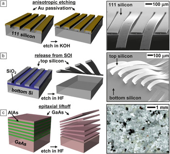
The technical scheme for high performance stretchable electronics involves two ideas: (1) the use of semiconductor nanomaterials, in shape-engineered forms, as the active components, and (2) circuit/device layouts that minimize strains in these and other “hard” constituent materials when integrated with “soft” elastomeric substrates. For the first, wafer-scale sources of semiconductor material, in bulk or thin-film form, serve as starting points for the “top down” fabrication of wires/ribbons/membranes.Reference Mack, Meitl, Baca, Zhu and Rogers48–Reference Sun, Khang, Hua, Hurley, Nuzzo and Rogers51 In nanoscale thicknesses, these structures have exceptionally low flexural rigidities (e.g., >1015 smaller than conventional wafers of corresponding materials) and experience minimal strains even when bent to small radii of curvature, both of which are consequences of elementary principles in mechanicsReference Jiang, Khang, Song, Sun, Huang and Rogers52, Reference Song, Jiang, Choi, Khang, Huang and Rogers53—the flexural rigidity is EH 3/12, where E is the elastic modulus, and H is thickness (∼0.5 mm for a wafer, and as small as ∼2 nm for a nanomembrane), and the maximum strain due to bending is ε = H/(2r) where r is the radius of curvature (ε ∼0.001% for H = 10 nm and r = 0.5 mm). Figure 1 summarizes three representative routes to this class of nanomaterial. The first (Figure 1a) uses anisotropic processing of a silicon wafer with (111) crystallographic orientation.Reference Mack, Meitl, Baca, Zhu and Rogers48, Reference Baca, Meitl, Ko, Mack, Kim, Dong, Ferreira and Rogers49 Here, reactive ion etching defines trenches with well-controlled widths and depths, oriented perpendicular to the (110) direction. Subsequent deposition of passivation layers (e.g., SiO2, Au) on the top surfaces and sidewalls of these trenches protects them during anisotropic etching of the exposed silicon with potassium hydroxide (KOH) or tetramethyl ammonium hydroxide (TMAH). This process removes material along planes of (110) at much higher rates (>100X) compared to (111), thereby releasing wires/ribbons/membranes with nanoscale thicknesses from the near-surface region of the wafer. The geometry of the trenches and the coverage of the passivation layers define the dimensions of these structures. Repeating these steps can convert nearly all of the material of the wafer into these types of elements or other nanostructured forms. Related schemes are applicable to other materials, such as GaAs and InP.Reference Sun, Khang, Hua, Hurley, Nuzzo and Rogers51 Advanced implementations with silicon have capabilities for releasing thick, multilayer stacks in a manner that yields bulk quantities of nanomaterials in a single process sequence.Reference Ko, Baca and Rogers50
Schematic illustrations (left) and corresponding images (right) of semiconductor nanoribbons and membranes derived from wafer-scale sources of material by lithographic patterning and undercut etching. (a) Anisotropic wet chemical etching of a silicon wafer with (111) orientation. The scanning electron microscope image on the right shows a collection of partially released ribbons (∼500 nm thickness). (b) Etching the exposed buried oxide of a silicon-on-insulator (SOI) wafer releases the top silicon to yield collections of nanoribbons (thicknesses of 300 nm shown here). (c) Etching sacrificial layers of AlAs in epitaxial multilayer stacks of GaAs/AlAs releases large quantities of GaAs nanomembranes. Reproduced with permission from Reference Reference Yoon, Jo, Chun, Jung, Kim, Meitl, Menard, Li, Coleman, Paik and Rogers63. ©2010, Nature Publishing Group.

A complementary approach uses layered materials formed by wafer bonding and polishing or controlled fracture,Reference Bruel54 or by epitaxial growth. The most common example starts with silicon-on-insulator (SOI) wafers.Reference Ahn, Kim, Lee, Zhu, Menard, Nuzzo and Rogers15, Reference Kim, Ahn, Kim, Lee, Kim, Yu, Nuzzo and Rogers16, Reference Choi, Song, Khang, Jiang, Huang and Rogers19, Reference Sun, Qin, Seo, Celler, Zhou and Ma55, Reference Qin, Yuan, Celler, Ma and Ma56 Undercut etching of the buried oxide with hydrofluoric acid, or the silicon support using the schemes of Figure 1a, releases the top Si layer with or without the insulator intact. The latter process appears in Figure 1b. Other examples of SOI-like structures include germanium-on-insulator (GOI), silicon-germanium-on-insulator (SGOI), as well as III–V semiconductors and many other combinations.Reference Schmidt and Eberl57–Reference Yuan, Shin, Qin, Sun, Bhattacharya, Lagally, Celler and Ma60 For the last class of material, epitaxial liftoff techniques can also be used.Reference Yablonovitch, Gmitter, Harbison and Bhat61, Reference Konagai, Sugimoto and Takahashi62 In a recent, advanced scheme, alternating layers of gallium arsenide (GaAs) and aluminum arsenide (AlAs), both grown epitaxially on a GaAs wafer, yield bulk quantities of GaAs nanoribbons/membranes (Figure 1c, right frame) upon selective removal of AlAs with hydrofluoric acid.Reference Yoon, Jo, Chun, Jung, Kim, Meitl, Menard, Li, Coleman, Paik and Rogers63 In this case, the wafer can be re-used for multiple growths, as in Figure 1c.
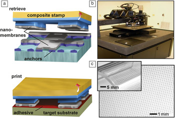
Nanomaterials, or even ultrathin, fully formed devices,Reference Chung, Kim, Kim, Wells, Jo, Ahmed, Jung, Won, Bower and Rogers64 generated using the schemes shown in Figure 1, can be integrated onto substrates of choice in a controlled, deterministic fashion by the techniques of transfer printing.Reference Meitl, Zhu, Kumar, Lee, Feng, Huang, Adesida, Nuzzo and Rogers65, Reference Feng, Meitl, Bowen, Huang, Nuzzo and Rogers66 An important feature of this process is that it exploits the known, lithographically defined positions and orientations of undercut-etched nanostructures, each anchored at its corners to the underlying wafer. Retrieval from these pre-determined sites, followed by release onto other substrates, can be accomplished with polydimethylsiloxane (PDMS) stamps. (Figure 2a) The procedure involves switching the strength of adhesion between these structures and PDMS from strong to weak states by exploiting viscoelastic and/or geometric effects.Reference Meitl, Zhu, Kumar, Lee, Feng, Huang, Adesida, Nuzzo and Rogers65–Reference Kim, Wu, Carlson, Jin, Kovalsky, Glass, Liu, Ahmed, Elgan, Chen, Ferreira, Sitti, Huang and Rogers68 Advanced implementations allow printing of many millions of structures per hour, in ambient conditions, with yields exceeding 99.99% and sub-micron positioning and overlay accuracy. A picture of an automated printing system with these and other capabilities appears in Figure 2b.Reference Yoon, Jo, Chun, Jung, Kim, Meitl, Menard, Li, Coleman, Paik and Rogers63Figure 2c shows images of an array of GaAs platelets printed with this tool onto a piece of plastic.Reference Park, Xiong, Kim, Elvikis, Meitl, Kim, Wu, Yoon, Yu, Liu, Huang, Hwang, Ferreira, Li, Choquette and Rogers23 Materials with thicknesses spanning the sub-nanometer level to tens of microns, and with lateral dimensions ranging from the nanometer to centimeter scale, can be manipulated in a similar fashion.Reference Chung, Kim, Kim, Wells, Jo, Ahmed, Jung, Won, Bower and Rogers64, Reference Kang, Kocabas, Kim, Cao, Meitl, Khang and Rogers69, Reference Unarunotai, Koepke, Tsai, Du, Chialvo, Murata, Haasch, Petrov, Mason, Shim, Lyding and Rogers70
Transfer printing provides a high speed, scalable method for deterministic assembly of semiconductor nanomaterials into organized layouts. (a) Schematic illustration of the printing process. (b) Image of an automated transfer printing tool, composed of a collection of precision, computer-controlled motion stages, and a high resolution imaging system for overlay registration. (c) Image of an array of GaAs membranes (250 × 250 μm) transfer printed onto a plate of glass and a thin, flexible sheet of plastic (inset). Reproduced with permission from Reference Reference Park, Xiong, Kim, Elvikis, Meitl, Kim, Wu, Yoon, Yu, Liu, Huang, Hwang, Ferreira, Li, Choquette and Rogers23. ©2009, American Association for the Advancement of Science.

Unconventional designs and stretchable electronics
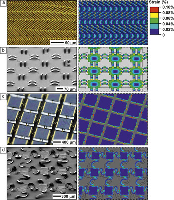
Interconnected assemblies of nanomaterials printed onto elastomeric substrates can yield stretchable electronic/optoelectronic devices.Reference Khang, Jiang, Huang and Rogers17–Reference Choi, Song, Khang, Jiang, Huang and Rogers19 Here, analytical and computational mechanics models help to define layouts that minimize strains in the semiconductors and other electronic materials, most of which fracture at strains of only ∼1%, or less.Reference Jiang, Khang, Song, Sun, Huang and Rogers52, Reference Song, Jiang, Choi, Khang, Huang and Rogers53 Some simple geometric routes to this goal are shown in Figure 3, presented as pairs of experimental images (left) and mechanics modeling of the associated strain distributions (right). The first example results from bonding a silicon nanomembrane to a bi-axially prestrained (∼4%) slab of rubber (Figure 3a)Reference Choi, Song, Khang, Jiang, Huang and Rogers19 to enable controlled buckling upon release of this strain. Compressive stress associated with release of the pre-strain causes non-linear buckling instabilities that create “wavy” configurations with “herringbone” layouts in the membrane. When a hard/soft materials construct of this type is stretched by amounts that do not exceed the pre-strain, the wavy structures change in shape to accommodate overall deformations in ways that involve minimal strains in the membrane. The elastomer support provides the overall restoring force. The maximum strain in the film εfilm is related to the pre-strain εpre byReference Jiang, Khang, Song, Sun, Huang and Rogers52, Reference Song, Jiang, Choi, Khang, Huang and Rogers53

Experimental images (left) and mechanics modeling (right) of four different classes of structures with controlled buckling for high performance stretchable electronics. (a) A silicon nanomembrane uniformly bonded to an elastomeric substrate adopts a “wavy,” herringbone morphology. Reproduced with permission from Reference Reference Choi, Song, Khang, Jiang, Huang and Rogers19. ©2007, American Chemical Society. (b) A similar membrane structured into a mesh layout and selectively bonded only at the nodes takes a form that involves suspended, arc-shaped bridges (interconnects). This design offers enhanced ranges of stretchability compared to the case in (a). (c) Exploiting elastomer substrates with features of surface relief matched to the nodes of the mesh structures improves the mechanics to enable both high areal coverage and a large range of stretchability. Reproduced with permission from Reference Reference Lee, Wu, Shi, Yoon, Park, Li, Liu, Huang and Rogers74. ©2011, John Wiley & Sons, Inc. (d) Advanced version of the structure in (b), where the interconnect bridges have non-coplanar serpentine shapes. Reproduced with permission from Reference Reference Kim, Song, Choi, Kim, Kim, Liu, Huang, Hwang, Zhang and Rogers21. ©2008, National Academy of Sciences.

where 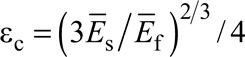 is the critical buckling strain and is very small, εc ∼ 0.036%, for the silicon film and PDMS substrate;
 and
 are the plane-strain moduli of the film and substrate, respectively. The strain in the film εfilm is reduced by 3x and 9x for εpre = 1% and 10%, respectively. Whitesides et al.Reference Bowden, Brittain, Evans, Hutchinson and Whitesides26 first reported this kind of geometry by direct evaporation of thin films of gold on PDMS. Subsequent efforts demonstrated the ability to use these and other related structures of gold on PDMS to achieve stretchable interconnects with remarkable levels of deformability (e.g., 200% stretchability) through combined effects of changes in geometry according to Equation 1 and motion of micro/nanocracks in the films.Reference Lacour, Jones, Suo and Wagner27–Reference Lacour, Chan, Wagner, Li and Suo29
An improvement on this approach involves (1) structuring of the membrane into an open mesh geometry and (2) selectively bonding the resulting mesh to the elastomer only at the nodes.Reference Ko, Stoykovich, Song, Malyarchuk, Choi, Yu, Geddes, Xiao, Wang, Huang and Rogers71, Reference Ko, Shin, Wang, Stoykovich, Lee, Kim, Ha, Huang, Hwang and Rogers72Figure 3b shows the result for a silicon nanomembrane patterned into an array of rectangular nodes (i.e., islands) connected by pairs of straight bridges that delaminate from the substrate to adopt arch-shaped structures upon release of the pre-strain. Under deformation, these non-coplanar bridges move in response to applied strains (for strains less than the pre-strain), thereby providing a certain level of mechanical isolation for the islands. The maximum strains in the bridges, εbridge, and islands, εisland, are related to εpre byReference Ko, Stoykovich, Song, Malyarchuk, Choi, Yu, Geddes, Xiao, Wang, Huang and Rogers71, Reference Song, Huang, Xiao, Wang, Hwang, Ko, Kim, Stoykovich and Rogers73

where L bridge is the bridge length, H bridge and H island are the bridge and island thicknesses, respectively, and E bridge and  are the Young’s modulus of the bridge and plane-strain modulus of the island, respectively. This strategy is most effective when the bridge thickness is much smaller than the bridge length, and the sizes of the islands are small compared to their separations. For H bridge= 50 nm and L bridge = 20 μm,Reference Song, Huang, Xiao, Wang, Hwang, Ko, Kim, Stoykovich and Rogers73 the strain in the bridge εbridge is reduced by 6x, 21x, and 90x for εpre = 1%, 10%, and 100%, respectively, and εbridge can be further reduced for thin and long bridges. The strain in the island εisland is the same as εbridge for islands and bridges having the same elastic modulus and thickness; and εisland can be further reduced as the island elastic modulus and thickness increase.
Some applications, such as those in stretchable photovoltaics, image sensors, and display/lighting modules, benefit from layouts that have high areal coverages of device islands. Such requirements can be addressed with a design modification that involves thin elastomer substrates with raised features of relief with lateral dimensions that match the sizes and layouts of the islands.Reference Song, Huang, Xiao, Wang, Hwang, Ko, Kim, Stoykovich and Rogers73 In this configuration, strains induced by deformations localize, almost entirely, to the recessed regions between the islands, corresponding to the positions of arc-shaped interconnects that buckle downward. Here, the maximum strains in the bridges and islands are related to εpre byReference Lee, Wu, Shi, Yoon, Park, Li, Liu, Huang and Rogers74

where L island and L trench are the length of the island and length of the trench between islands, respectively. For H bridge= 50 nm and L island= L trench= 20 μm, which gives 25% areal coverage of device islands, the strain in the bridge εbridge is reduced by 230x for εpre =100%. For the same total length L island+ L trench= 40 μm but a much smaller length of the trench L trench = 5 μm (i.e., L island = 35 μm), the areal coverage of device islands increases to 77%, and the strain in the bridge εbridge is reduced by 150x for the same pre-strain εpre =100%. An example of this appears in Figure 3c.Reference Lee, Wu, Shi, Yoon, Park, Li, Liu, Huang and Rogers74
Extreme stretchability (>100%) can be accomplished by replacing the straight bridge interconnects with those that have serpentine shapes, as in Figure 3d.Reference Kim, Song, Choi, Kim, Kim, Liu, Huang, Hwang, Zhang and Rogers21, Reference Kim, Bae, Kim, Cheng, Kim, Kim, Li, Wu, Kim, Hong, Huang, Pop and Rogers75 Here, the applied strain can significantly exceed the pre-strain. For an applied strain ε = 106%, the maximum strain in the serpentine bridges is only 0.35% (i.e., a reduction of strain by 300x).Reference Kim, Bae, Kim, Cheng, Kim, Kim, Li, Wu, Kim, Hong, Huang, Pop and Rogers75 As in the other examples, strong and weak bonding at the sites of the islands and interconnects, respectively, leads to non-coplanar layouts optimally suited for accommodating strain. Coplanar schemes have been explored by other groups using fabrication and integration strategies that are different than, but complementary to, those discussed here.Reference Brosteaux, Axisa, Gonzalez and Vanfleteren30–Reference Kim, Son and Ziaie33, Reference Gray, Tien and Chen76 In all cases, practical applications demand encapsulants for mechanical protection and environmental barriers over the entire area. As demonstrated in systematic experimentalReference Kim, Liu, Kim, Wu, Song, Kim, Huang, Hwang, Zhang and Rogers77 and modeling studies, low modulus materials that provide minimal constraints on the motions of the interconnects are desirable. The stretchability in this case can be determined analytically as a function of the pre-strain and the elastic modulus of the encapsulation layer.Reference Wu, Liu, Song, Huang, Hwang, Zhang and Rogers78 We note that for any design, the behavior depends strongly on the detailed geometries and materials.
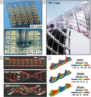
These simple concepts in materials, assembly/integration, and mechanics immediately enable diverse classes of stretchable electronic and optoelectronic devices. Figure 4 provides some examples. A system that exploits the mechanics of Figure 3a appears in Figure 4a.Reference Kim, Ahn, Choi, Kim, Kim, Song, Huang, Liu, Lu and Rogers20 Here, an ultrathin (∼1.7 μm), complementary metal oxide silicon (CMOS) circuit that uses silicon nanomembranes as active materials in a neutral mechanical plane layout bonds in a “wavy” configuration to an underlying elastomer. When mildly stretched, the amplitudes and wavelengths of the waves reduce and increase, respectively, in a manner that avoids significant strains in the devices. Although full-area coverage of circuit elements is possible with this design, the range of stretchability is modest (i.e., 20% or less). Figure 4b displays an example using the scheme of Figure 3c, which retains the coverage capability but expands stretching to dimensional changes of tens of percent.Reference Lee, Wu, Shi, Yoon, Park, Li, Liu, Huang and Rogers74 Serpentine interconnects further improve the mechanics, as demonstrated with an array of ultrathin (∼2 μm), microscale inorganic light-emitting diodes (μ-ILEDs) on a rubberband, in Figure 4c.Reference Kim, Kim, Xiao, Kim, Park, Panilaitis, Ghaffari, Yao, Li, Liu, Malyarchuk, Kim, Le, Nuzzo, Kaplan, Omenetto, Huang, Kang and Rogers24 Mechanics modeling (Figure 4d) show shear strains approaching 50% for the case of twisting by 720 degrees. Related devices show ranges of stretchability that approach the fracture limits of the PDMS substrates (i.e., ∼200%) when the maximum strain in the devices is only 1%.
Examples of stretchable silicon circuits, AlInGaP light-emitting diodes and GaAs photovoltaics. (a) Two-dimensional wavy complementary metal oxide silicon (CMOS) circuits, in as-fabricated (top) and deformed (bottom) configurations. Reproduced with permission from Reference Reference Kim, Ahn, Choi, Kim, Kim, Song, Huang, Liu, Lu and Rogers20. ©2008, American Association for the Advancement of Science. (b) An array of GaAs photovoltaic microcells on a structured elastomer substrate. Reproduced with permission from Reference Reference Lee, Wu, Shi, Yoon, Park, Li, Liu, Huang and Rogers74. ©2011, John Wiley & Sons, Inc. (c) Array of GaAs microscale inorganic light-emitting diodes (μ-ILEDs) in a flat state and twisted by 360° and 720°. (d) Strain distributions in the twisted substrates, calculated by 3D finite element modeling for the case of the 720° twist. Reproduced with permission from Reference Reference Kim, Kim, Xiao, Kim, Park, Panilaitis, Ghaffari, Yao, Li, Liu, Malyarchuk, Kim, Le, Nuzzo, Kaplan, Omenetto, Huang, Kang and Rogers24. ©2010, Nature Publishing Group.

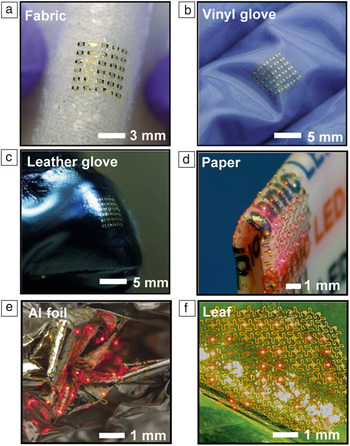
In addition to stretchability, the mechanics enables mounting of devices on nearly any class of substrate, flat or curved. Integration can be further facilitated by elastomeric planarization and adhesive layers that provide some mechanical decoupling of deformations in the underlying substrate from those in the mounted circuit. Figure 5 shows, as examples, electronic and optoelectronic devices integrated into substrates ranging from fabric (Figure 5a), vinyl (Figure 5b), leather (Figure 5c), and paper (Figure 5d) to sheets of aluminum foil (Figure 5e) and leaves from a tree (Figure 5f).Reference Kim, Kim, Wu, Liu, Song, Kim, Huang, Hwang and Rogers22, Reference Kim, Kim, Xiao, Kim, Park, Panilaitis, Ghaffari, Yao, Li, Liu, Malyarchuk, Kim, Le, Nuzzo, Kaplan, Omenetto, Huang, Kang and Rogers24 Some of these instances have clearly envisioned uses, such as in “instrumented” surgical gloves (Figure 5b) or paper-based diagnostic devices (Figure 5d); others are purely exploratory (Figure 5f), as demonstrators for unusual engineering options that suggest opportunities in biointegration, as discussed subsequently.
Examples of stretchable electronics/optoelectronics integrated onto diverse substrates, facilitated by the use of thin, strain-isolating adhesives. (a) Silicon CMOS circuits on a piece of fabric (a), and on vinyl (b) and leather (c) gloves. Interconnected array of microscale inorganic light-emitting diodes (μ-ILEDs) on a piece of folded paper (d), a sheet of aluminum foil (e), and a leaf (f). (a–c) Reproduced with permission from Reference Reference Kim, Kim, Wu, Liu, Song, Kim, Huang, Hwang and Rogers22. ©2009, John Wiley & Sons, Inc. (d–f) Reproduced with permission from Reference Reference Kim, Kim, Xiao, Kim, Park, Panilaitis, Ghaffari, Yao, Li, Liu, Malyarchuk, Kim, Le, Nuzzo, Kaplan, Omenetto, Huang, Kang and Rogers24. ©2010, Nature Publishing Group.

Bioinspired cameras
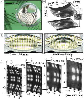
Regarding system-level device examples, we focus on two classes of technology that are not well-addressed by other forms of electronics: digital cameras with bioinspired, hemispherical layouts, and biointegrated devices for clinical use in cardiology, neurology, and other related areas of medicine.Reference Kim, Viventi, Amsden, Xiao, Vigeland, Kim, Blanco, Panilaitis, Frechette, Contreras, Kaplan, Omenetto, Huang, Hwang, Zakin, Litt and Rogers42–Reference Kim, Lu, Ma, Kim, Kim, Wang, Wu, Won, Tao, Islam, Yu, Kim, Chowdhury, Ying, Xu, Li, Chung, Keum, McCormick, Liu, Zhang, Omenetto, Huang, Coleman and Rogers45, Reference Ko, Stoykovich, Song, Malyarchuk, Choi, Yu, Geddes, Xiao, Wang, Huang and Rogers71, Reference Shin, Jung, Malyarchuk, Song, Wang, Ko, Huang, Ha and Rogers79–Reference Jung, Xiao, Malyarchuk, Lu, Li, Liu, Yoon, Huang and Rogers81 Corresponding to the first area, Figure 6a shows an electronic “eyeball” camera that incorporates a hemispherically curved photodetector array with the size and shape of the human eye.Reference Ko, Stoykovich, Song, Malyarchuk, Choi, Yu, Geddes, Xiao, Wang, Huang and Rogers71 The fabrication starts with the formation of a planar, interconnected array of silicon photodiodes in a mesh geometry to exploit the mechanics of Figure 3b. Controlled compressive deformation using a shaped, thin elastomer stamp accomplishes a planar to hemispherical geometry transformation and transfer to the concave surface of a glass support. Mounting the resulting component on a printed circuit board connects it to external data acquisition hardware; coupling a simple, plano-convex lens fixed in a transparent hemispherical shell completes the camera. The fields of view, levels of aberration, and illumination uniformity that are possible with this hemispherical design all exceed those achievable with conventional, flat photodetector arrays when similarly simple optics are used.Reference Rim, Catrysse, Dinyari, Huang and Peumans34, Reference Malyarchuk, Jung, Rogers, Shin and Ha82Figure 6b presents a picture captured with this camera, rendered in the hemispherical geometry of the detector (top), and as a planar projection (bottom); the actual object appears in the right inset. The key feature of this device is that the shape of the photodetector array approximately matches that of the image formed with the lens (i.e., the curved surface associated with the imaging process, known as the Petzval surface). Precise matching involves surfaces in the shape of elliptic paraboloids.Reference Jung, Shin, Malyarchuk, Ha and Rogers80, Reference Malyarchuk, Jung, Rogers, Shin and Ha82 Other published routes to similar types of layouts include expandable silicon chip arrays, connected by spiral filaments or leaf-springs, and printed organic devices.Reference Rim, Catrysse, Dinyari, Huang and Peumans34–Reference Lee and Szema37, Reference Huang and Peumans83 Although functioning cameras have been not been achieved in these cases, such procedures appear to have potential as an alternative path to devices of the type of Figure 6a–b.
(a) Image of a hemispherical electronic eye camera. (b) Picture of an eye captured using the camera shown in (a), rendered in the hemispherical geometry of the photodetector array (top), and in a planar projection (bottom). Inset shows the original picture. (c) Images of an electronic eye camera that incorporates a photodetector array with tunable curvature, in flat (left) and convex (right) states. (d) Pictures of a test pattern captured using such a tunable device, at four different zoom magnification settings (r, radius of curvature). Reproduced with permission from Reference Reference Jung, Xiao, Malyarchuk, Lu, Li, Liu, Yoon, Huang and Rogers81. ©2011, National Academy of Sciences.

A deficiency of all of these reported designs is that the detector geometries are fixed. As a result, wide-range, tunable zoom cannot be realized because the detectors cannot follow the associated changes in the Petzval surfaces. The principles of stretchable electronics, however, enable detector curvature that can be adjusted continuously to provide a level of functionality that is not found in nature (i.e., unlike imaging organs found in biology). An example of this capability (Figure 6c) uses a photodiode array with interconnects in the design of Figure 3c, supported by a thin PDMS membrane clamped at its edges by a circular fixture.Reference Jung, Xiao, Malyarchuk, Lu, Li, Liu, Yoon, Huang and Rogers81 The radius of curvature of the membrane can be precisely controlled using a simple, miniaturized hydraulic system. The associated mechanics result in an overall hemispherical shape over a wide tuning range, confirmed by measurements as well as mechanics and optics modeling.Reference Jung, Xiao, Malyarchuk, Lu, Li, Liu, Yoon, Huang and Rogers81 A quantitative understanding of the shape of the detector array and the positions of the detectors is important. The radius of the hemispherical shape can be obtained analytically in terms of the applied pressure.Reference Jung, Xiao, Malyarchuk, Lu, Li, Liu, Yoon, Huang and Rogers81d denotes the initial diameter of the membrane and z the height of the hemisphere after the applied pressure. A detector pixel at an initial radial position r, relative to the membrane center, moves to a new radius r′ and height z′ given by,

Coordinating this adjustment with the magnification setting of a tunable, fluidic imaging lens yields a hemispherical camera capable of adjustable zoom, as shown in the sequence of pictures in Figure 6d.
Biointegrated surgical tools
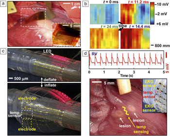
A second area of interest for system-level applications is in electronics that intimately and non-invasively laminate onto the surfaces of human tissue (internal or external) in a mode referred to as biointegration.Reference Lacour, Tsay, Wagner, Yu and Morrison38, Reference Graudejus, Yu, Jones, Morrison and Wagner39, Reference Kim, Viventi, Amsden, Xiao, Vigeland, Kim, Blanco, Panilaitis, Frechette, Contreras, Kaplan, Omenetto, Huang, Hwang, Zakin, Litt and Rogers42–Reference Kim, Lu, Ma, Kim, Kim, Wang, Wu, Won, Tao, Islam, Yu, Kim, Chowdhury, Ying, Xu, Li, Chung, Keum, McCormick, Liu, Zhang, Omenetto, Huang, Coleman and Rogers45 Traditional devices rely on interfaces consisting of small numbers of rigid point contacts, each with separate cables that connect to remotely located rigid electronic systems.Reference Campbell, Jones, Huber, Horch and Normann84, Reference Ives, Mirsattari and Jones85 The principles of stretchable electronics, by contrast, enable devices that are themselves tissue-like in their physical properties (i.e., thin, soft, curvilinear), with the ability to follow the motions of the body without any significant mechanical or mass loading effects. These characteristics enable conformable adhesion with electrical, thermal, optical, and chemical access, and robust binding without irritation.Reference Kim, Lu, Ma, Kim, Kim, Wang, Wu, Won, Tao, Islam, Yu, Kim, Chowdhury, Ying, Xu, Li, Chung, Keum, McCormick, Liu, Zhang, Omenetto, Huang, Coleman and Rogers45 Such devices can provide thousands or millions of interface points, with local electronics for advanced processing, monitoring, stimulating, or other functions, along with multiplexed readout to minimize the number of wire connections.Reference Viventi, Kim, Moss, Kim, Blanco, Annetta, Hicks, Xiao, Huang, Callans, Rogers and Litt43 In one example of a device that offers extreme flexibility, shown in Figure 7a, a sheet of silicon electronics, consisting of more than 2000 nanomembrane transistors, laminates onto the epicardial surface (i.e., the outer layer of the heart), much like a piece of plastic wrap, to perform high speed mapping of cardiac electrophysiology.Reference Viventi, Kim, Moss, Kim, Blanco, Annetta, Hicks, Xiao, Huang, Callans, Rogers and Litt43 Here, electrocardiograms (ECGs) measured by each node in the sensor array are collected by data acquisition systems and converted into color maps in real-time. Figure 7b shows a representation of a time sequence of electrophysiological maps collected with a typical device from the healthy, beating heart of a live porcine animal model. High speed multiplexing transistors and local amplification ICs at each sensor location enable this operation. This technology provides much higher resolution, with much shorter data collection times than existing clinical approaches, all of which involve manual positioning of single-point electrode probes at different locations across the heart for mapping in a point-by-point fashion. Measurements of this type represent critical steps of open-heart surgical procedures that involve locating, and then removing, regions of the tissue that are responsible for certain forms of arrhythmias. Technologies that can improve this process are, therefore, clinically valuable.
(a) Image of an electrophysiological (EP) sensor array conformally laminated onto the epicardial surface of a porcine animal model. The inset provides a magnified view. (b) Mapping results at four different times (t), where the measured surface potential is displayed as a color map. Reproduced with permission from Reference Reference Viventi, Kim, Moss, Kim, Blanco, Annetta, Hicks, Xiao, Huang, Callans, Rogers and Litt43. ©2010, American Association for the Advancement of Science. (c) A multifunctional “instrumented” balloon catheter in its deflated (top) and inflated (bottom) states. The device includes EP and rf ablation electrodes, temperature sensors, pressure sensors, and arrays of microscale inorganic light-emitting diodes (μ-ILEDs). (d) Electrocardiogram recorded by a pair of EP electrodes positioned on the right ventricle (RV) of a rabbit heart (top) and an image of lesions created by rf ablation (bottom). The inset shows EP and rf ablation electrodes and a temperature sensor. Reproduced with permission from Reference Reference Kim, Lu, Ghaffari, Kim, Lee, Xu, Wu, Kim, Song, Liu, Viventi, de Graff, Elolampi, Mansour, Slepian, Hwang, Moss, Won, Huang, Litt and Rogers44. ©2011, Nature Publishing Group.

Another mode of operation involves endocardial access, using devices that insert into the heart remotely through arteries or veins. The concepts of stretchable electronics can address this circumstance as well through integration of circuits and integrated sensors onto the surfaces of otherwise conventional catheter balloons. In this approach, device functionality on a deflated catheter is delivered to the interior of the heart via an artery or vein. Inflation then softly presses the deformable membrane of the balloon against the endocardial surface in a configuration where the surgeon can perform a range of sensing and therapeutic operations. An example of such a multifunctional, instrumented balloon device appears in Figure 7c, where the functionality ranges from ECG mapping to temperature and tactile sensing, to flow monitoring, tissue ablation, and LED-based activation of photosensitive drugs.Reference Kim, Lu, Ghaffari, Kim, Lee, Xu, Wu, Kim, Song, Liu, Viventi, de Graff, Elolampi, Mansour, Slepian, Hwang, Moss, Won, Huang, Litt and Rogers44 The images show the balloon in deflated (top) and inflated (bottom) states. ECG traces recorded from the right ventricle of a porcine model appear in Figure 7d (top frame). One of the most common procedures to eliminate aberrant tissue uses radio frequency (rf) energy to induce lesions on the surface of heart and into the depth of the tissue by controlled amounts (Figure 7d, bottom frame). The process relies mainly on Joule heating associated with the current induced by rf ablation electrodes. The applied power and time, the geometry of the electrodes, and their degree of contact with the tissue determine the lesion size and depth. In situ temperature, flow, and physical contact monitoring during ablation, coupled with quantitative models for heat generation and thermal diffusion are, therefore, important for executing this type of therapy. All of the necessary functionality can be integrated directly with the balloon, using the concepts of Figure 3d, as illustrated in Figure 7c–d. Such tools have the potential to reduce risk and improve effectiveness in cardiac surgeries.
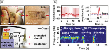
In a most recent and advanced demonstration of the concepts of biointegrated devices, electronics have been achieved with physical properties, ranging from modulus to degree of stretchability, areal mass density, thickness, and flexural rigidity, all matched to the epidermis. Devices in this format can laminate onto the surface of the skin, much like a temporary transfer tattoo, to provide various types of healthcare and non-healthcare related functions.Reference Kim, Lu, Ma, Kim, Kim, Wang, Wu, Won, Tao, Islam, Yu, Kim, Chowdhury, Ying, Xu, Li, Chung, Keum, McCormick, Liu, Zhang, Omenetto, Huang, Coleman and Rogers45 An image of a demonstration platform for this type of epidermal electronic system (EES) appears in Figure 8a; the structure includes antennas, wireless power coils, silicon nanomembrane metal oxide semiconductor field-effect transistors (MOSFETs) and diodes, strain and temperature gauges, along with rf inductors, capacitors, and oscillators. The mechanics designs, which represent advanced versions of the layout shown in Figure 3d,Reference Kim, Song, Choi, Kim, Kim, Liu, Huang, Hwang, Zhang and Rogers21 and substrate materials yield effective moduli in the range of ∼100 kPa and thicknesses of ∼30 μm (Figure 8a).Reference Kim, Lu, Ma, Kim, Kim, Wang, Wu, Won, Tao, Islam, Yu, Kim, Chowdhury, Ying, Xu, Li, Chung, Keum, McCormick, Liu, Zhang, Omenetto, Huang, Coleman and Rogers45 With these properties, simple lamination, without straps or glue layers, leads to conformal contact with the skin to yield robust adhesion even under significant deformation (Figure 8a). The bottom frame in Figure 8a shows a collapsed EES after peeling a device away from the skin; the inset shows a cross-sectional schematic view of the system and the low modulus (∼50 kPa) substrate, which is based on silicone elastomer. This contact also yields low-impedance coupling of electrodes for electrophysiological measurements, without the use of conductive gels or penetrating pins. Figure 8b presents measurement results for ECG (top) and electroencephalography (EEG; bottom) recorded with EES mounted on the chest and forehead, respectively, to monitor activity of the heart and brain, respectively. The ECG measurement electrodes use local amplification to yield data with clear QRS signatures (Q, R, and S waves) and signal-to-noise ratios that compare favorably to those obtained with conventional bulk electrodes and conductive gels. Likewise, the EEG traces exhibit characteristic alpha rhythms when the subject’s eyes are closed. With eyes open, these rhythms disappear, as expected.Reference Goldman, Stern, Engel and Cohen86 Data in these and other cases can contain sufficient information for human-machine interfaces, as recently demonstrated through a simple computer game controller based on EES measurements of muscle activity near the throat.Reference Kim, Lu, Ma, Kim, Kim, Wang, Wu, Won, Tao, Islam, Yu, Kim, Chowdhury, Ying, Xu, Li, Chung, Keum, McCormick, Liu, Zhang, Omenetto, Huang, Coleman and Rogers45
(a) Images of an epidermal electronic system (EES) mounted on human skin, in compressed (left) and stretched (right) states. The EES collapses under its own weight after detachment from the skin (bottom). The inset shows a schematic cross-sectional layout, highlighting the thin construction and the neutral mechanical plane (NMP) design of the polyimide (PI) and device. (b) Electrocardiogram recorded from the chest using an EES (left) and magnified view (right) that shows clear Q, R, and S waveforms. The bottom frame shows spectrographs of alpha rhythm recordings with eyes closed and open for the first 10 and subsequent 10 seconds, respectively. Reproduced with permission from Reference Reference Kim, Lu, Ma, Kim, Kim, Wang, Wu, Won, Tao, Islam, Yu, Kim, Chowdhury, Ying, Xu, Li, Chung, Keum, McCormick, Liu, Zhang, Omenetto, Huang, Coleman and Rogers45. ©2011, American Association for the Advancement of Science.

Conclusions
The field of stretchable electronics is evolving rapidly, driven mainly by advances in materials and assembly techniques. The development path relies critically on quantitative mechanics design, at a level of importance that is comparable to circuit design in conventional electronics. An emerging baseline of capabilities now enables innovative and realistic engineering efforts, some of which are yielding sophisticated system-level demonstrators in important areas of application that cannot be addressed with any other approach. A valuable perspective on this field is that dominant trends in the semiconductor industry are, in an unexpected way, coincident with demands associated with approaches such as those in Figure 2. In particular, the drive toward smaller and thinner devices to improve operating speeds and levels of integration in conventional ICs has immediate and direct benefits in stretchable electronics because these same geometries lead to favorable mechanical properties. Such synergies greatly enhance the prospects not only for biointegrated electronicsReference Kim, Kim, Xiao, Kim, Park, Panilaitis, Ghaffari, Yao, Li, Liu, Malyarchuk, Kim, Le, Nuzzo, Kaplan, Omenetto, Huang, Kang and Rogers24, Reference Lacour, Tsay, Wagner, Yu and Morrison38–Reference Sekitani, Zschieschang, Klauk and Someya40, Reference Kim, Lu, Ghaffari, Kim, Lee, Xu, Wu, Kim, Song, Liu, Viventi, de Graff, Elolampi, Mansour, Slepian, Hwang, Moss, Won, Huang, Litt and Rogers44, Reference Kim, Lu, Ma, Kim, Kim, Wang, Wu, Won, Tao, Islam, Yu, Kim, Chowdhury, Ying, Xu, Li, Chung, Keum, McCormick, Liu, Zhang, Omenetto, Huang, Coleman and Rogers45 and bioinspired device design,Reference Lee and Szema37, Reference Shin, Jung, Malyarchuk, Song, Wang, Ko, Huang, Ha and Rogers79–Reference Jung, Shin, Malyarchuk, Ha and Rogers80 as described here, but also for many other classes of stretchable, curvilinear technologies in portable photovoltaics,Reference Lee, Wu, Shi, Yoon, Park, Li, Liu, Huang and Rogers74 conformal thermoelectric,Reference Leonov, Torfs, Vullers and Hoof87 curvilinear active antennas,Reference Pryce, Aydin, Kelaita, Briggs and Atwater88 solid-state lighting systems,Reference Park, Xiong, Kim, Elvikis, Meitl, Kim, Wu, Yoon, Yu, Liu, Huang, Hwang, Ferreira, Li, Choquette and Rogers23, Reference Kim, Kim, Xiao, Kim, Park, Panilaitis, Ghaffari, Yao, Li, Liu, Malyarchuk, Kim, Le, Nuzzo, Kaplan, Omenetto, Huang, Kang and Rogers24 energy harvesters,Reference Qi, Kim, Nguyen, Lisko, Purohit and McAlpine41, Reference Feng, Yang, Liu, Wang, Dagdeviren, Liu, Carlson, Li, Huang and Rogers89 and others. At the same time, many compelling opportunities for continued basic research follow from the unusual and extreme materials heterogeneity inherent in these systems. The topics range from synthesis and physics of semiconductor nanomaterials, to soft adhesion and self-assembly, to micro/nanomechanics and fracture science, to heat transfer and energy conversion processes, to bio-compatible materials and interfaces in biotic/abiotic systems. These combined attributes in science and technology suggest that the field of stretchable electronics will remain a fertile, expanding area for research and development for many years to come.
Acknowledgments
This material is based upon work, the main components of which were supported by the Department of Defense, the National Science Foundation, and the Department of Energy. N.L. acknowledges support from a Beckman Institute postdoctoral fellowship. D.K. acknowledges support from a Global Frontier Research Center for Advanced Soft Electronics.