I. INTRODUCTION
The continual development of Microwave Integrated Circuits (MIC)/Monolithic Microwave Integrated Circuits (MMIC)/Microelectromechanical systems (MEMS) circuits and subsystems mandates the development of topologies for microwave and millimeter-wave systems using planar lines. Microstrip and Coplanar waveguide (CPW) are the most commonly used transmission lines. The CPW transmission lines are preferred where rapid characterization, ease of implementation for hybrid connections, minimization of substrate thickness, and radiation effects are to be considered. Most packages use microstrip connectors which necessitates the incorporation of transitions. This demands implementation of etching techniques in the ground plane or via hole for keeping the ground plane at the same potential. This leads to increased complexity as it requires wafer thinning and backside processing along with extensive design and process optimization for selecting the dimensions and distribution of vias.
This problem can be alleviated by introducing uniform conductor backing at the backside of the wafer [Reference Tien, Tzuang, Peng and Chang1]. This reduces dispersion, improves mechanical strength, provides convenient DC biasing, eliminates vias, reduces parasitic inductance, and heat sink [Reference Jackson2]. The circuit can be viewed and analyzed as a system of three coupled slot lines. The major problems with this assembly include leakage of power into surface waves, unexpected cross talk, and unwanted coupling. This is due to the undesired microstrip mode setting up beneath the substrate [Reference Shigesawa, Tsuji and Oliver3]. This can be circumvented by modifying the ground plane width so as to eliminate microstrip and odd mode wave propagation. Resulting CPW mode has to be propagated and should be transformed into microstrip mode or vice versa by reducing mismatch through transition. Reported transitions so far with via and via-less topologies lack compactness, possesses narrower bandwidth, and realized on thinner substrate. [Reference Braucher, Robertson, East and Katehi4] The topology presented by Singh et al. [Reference Singh and Pal5] uses transitions from finite ground-conductor backed-CPW (FG-CBCPW) to microstrip with improved characteristics but provides narrow bandwidth. Zheng et al. [Reference Zheng, Papapolymerou and Tenzeris6] proposed topology on silicon with wider bandwidth but could not achieve good return loss characteristics. This article is the extension of the work carried out by Zheng and proposes a modified structure to achieve better characteristics in wider bandwidth on thicker substrates. Method of moments (MoM) was used to optimize the design and validation of the experimental results.
II. TRANSITION CIRCUIT DESIGN
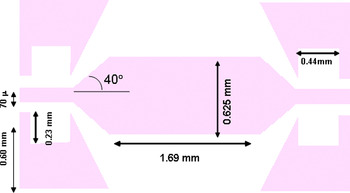
The structure consists of FG-CB-CPW section, conductor backed CPW-to microstrip transition section, and a microstrip section. In the intermediate section, the width of the CPW signal line is gradually increased to match the width of the microstrip line. At the same time, the gap between the ground planes and the signal line is widened to retain 50 Ω characteristics impedance along with minimal reflections. Transition angle is kept around 40° (400 µm), the ground plane width <λ/2 (GW ≈ 600 µm), and the CPW length around 0.13 λ (L ≈ 500 µm). Ground plane widths are optimized so that parallel plate and higher order modes can be avoided. Matched CPW configuration of G/W/G having dimensions of 40/70/40 µm is chosen to facilitate testing. High-resistivity silicon substrate (ɛ r = 11.7) with ρ > 8 kΩ cm with standard Complementary metal-oxide semiconductor (CMOS) oxide stack and nitride are used for simulation. The designed circuit is realized on 25 mils alumina substrate (Fig. 1).
Via-less FG-CB-CPW to microstrip transition.

Finite ground plane width provides riddance from unwanted parallel-plate modes that are triggered in the substrate between the coplanar lines and the ground plane.
III. SIMULATIONS AND EXPERIMENTAL RESULTS
Full-wave simulations for various combinations of geometrical parameters were performed using MoM techniques to reduce the insertion loss and to optimize the design in terms of size and operating bandwidth. Fabrication of the same device is carried out on alumina substrate. Measurement was performed using Agilent 8361 vector network analyzer attached with cascade probe station.
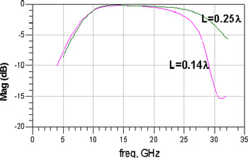
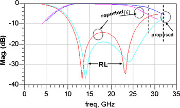
Figure 2 shows the comparison of simulated result for transition with different CPW lengths. The need for optimization of length can be seen for better bandwidth performance of the topology. The simulated performance (keeping the reported substrate thickness) of the proposed topology is compared with the suggested topology by Zheng et al. [Reference Zheng, Papapolymerou and Tenzeris6] in Fig. 3. As evident from the figure, return and insertion losses are better in the proposed topology. Also electrical performances of reported topology degrade on thicker substrates and needs extensive optimization.
Simulated insertion loss versus frequency for different length sections.

Simulated results comparison of proposed versus reported topology.

The role of the transition angle as shown in Fig. 1 is also studied. As the angle decreases, the transition between the conductor backed CPW (CB-CPW) to microstrip becomes smoother resulting in reduced insertion loss. An optimum value of 40° is chosen to compensate for the other effects. The design on silicon was replicated on 25 mils alumina substrate using standard lithography techniques. The reduction of substrate thickness will further enhance circuit performance by eliminating the undesired mode associated with thicker substrate. The cut-off frequency and other electrical performances can be enhanced by reducing the substrate thickness from the designed 675 µm.
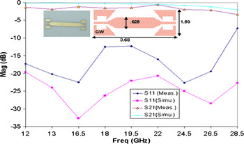
The result demonstrates bandwidth of >100% with maximum insertion loss of 1.5 dB and return loss better than 10 dB on 25 mil alumina substrate. Insertion loss variations, as shown in Fig. 4, are attributed to the losses associated with connectors and calibration-related errors. Discrepancy in return loss can be mitigated by eliminating assembly losses as well as keeping tight fabrication tolerances. Results clearly demonstrate the robustness of the circuit and same design can be replicated on various substrates, with nearby permittivity and thickness, without carrying out optimization.
Comparison of results on alumina substrate.

IV. CONCLUSION
In this article, a novel FG-CB CPW to microstrip transition was presented which can be easily incorporated in other technologies also. Proposed transitions find wide range of applications ranging from packaging to characterization due to its ease of implementation and compatibility with RF systems. The simulations and measurements showed wide band performance up to 28 GHz on 25 mils substrate with maximum loss of 2 dB which can be further improved by proper calibration and maintaining tight fabrication tolerances. This is the first time a transition on thicker substrate has been reported which caters for more than 100% bandwidth. This transition will find extensive application in MMIC-, MIC-, and MEMS-related devices for applications such as vertically integrated circuits requiring the flexibility to use combination of planar technologies.
 Kamaljeet Singh received master degree in microwaves from Delhi University in 1999 and received his Ph.D. degree in physics in 2010. He joined ISRO Satellite Center, Bangalore in 1999 where he worked in receiver division. From august 2006 onwards he is working in RF MEMS area at Semi-Conductor Laboratory, Chandigarh. His current research interests are in design of RF-MEMS and passive circuits for communication systems.
 K. Nagachenchaiah received degree in electronics and communication engineering from Andhra University and masters in computation and control engineering from IIT Kharagpur. He joined Space Applications Centre, Ahmedabad in 1974 and was involved in the design and development of various optical infrared remote sensors for aircraft and spacecraft platforms, ground-based instruments, and sensor test facilities. He has been honoured with various prestigious awards for his pioneer work in spacecraft technology. He is a distinguished scientist and actively involved in developmental activities related to RF-MEMS at SCL.