I. INTRODUCTION
As consequence of the increasing availability of nanomaterials, new classes of functional materials have entered the R&D landscape. The use of materials based on carbon nanotubes (CNT) has risen to become one of the most emblematic examples as they appear to be a promising building block for a large variety of nanotechnologies. Carbon nanotubes are cylinder-like structures made of rolled-up graphene sheets. Actually, they are one of the most-studied nanomaterials, owing to their high strength [Reference Overney, Zhong and Tomanek1], good electrical conductivity [Reference Yao, Postma, Balents and Dekker2], and excellent thermal conductivity [Reference Che, çagin and Goddard3]. Important applications include CNT-based composite polymer to improve conductive properties [Reference Flahaut, Peigney, Laurent, Marlière, Chastel and Rousset4] or enhance microwave performances such as those to alleviate the problem of electrical charging in dielectrics used for electrostatic actuation of RF-MEMS [Reference Bordas5] and in composite doped polymers in order to synthesize broadband microwave absorbing or shielding materials [Reference Pacchini, Idda, Dubuc, Flahaut and Grenier6]. Hence, the motivation to create the layout or topology of the CNT network will depend on the application, and so, for instance, a sensor based on CNTs should essentially be formed with single-walled carbon nanotubes (SWNTs) for semiconducting properties and with minimal percolation path [Reference Yun, Soo, Joondong, Shin and Park7]. On the other hand, interconnects or electrodes materials would require higher density and metallic properties of CNTs by using essentially the multi-walled carbon nanotubes (MWNTs) to maximize current transport capacity [Reference Hellstrom, Lee and Bao8]. It has been recently reported that MWNTs were successfully printed using a commercial desktop inkjet printer [Reference Kordas9]. However, the MWNTs exhibit essentially conducting properties in comparison with double-walled carbon nanotubes (DWNTs) that present semiconducting and conducting properties. The latter can be implemented in electronic devices with tunability properties.
On the other hand, inkjet printing technology is experiencing an increasingly central role in large consumer electronics manufacturing as selective transfer process. Recently, its use has been broadened to prototyping of circuits in microwave range [Reference Li, Rongwei, Daniela, Wong and Manos10]. Inkjet printing of DWNTs has been demonstrated to yield good control on pattern linewidth and uniformity of the printed pattern at low manufacturing costs. Current and future electronics systems, and in particular, radio-frequency (RF) ones, demand multiple functionalities while guaranteeing miniaturization, reliability, and temperature stability.
At this date, only a few preliminary studies have been reported on MWNTs-based inkjet printing and characterizations of such material as conductive pattern at low and especially at high frequency [Reference Gaggliardi11, Reference Seong12].
The development carried out to obtain thin film layers endowed with enhanced functionalities such as the tunability of conductive properties in the specific case of inkjet-printed DWNTs layer is herein presented. DWNT ink has been investigated in order to obtain a good dispersion of DWNTs in solution suitable for inkjet printing, and monitor the long-term stability. The electrical characteristics of the networks of DWNTs have been evaluated at DC, low, and high frequency.
II. EXPERIMENTAL SETUP AND SAMPLE PREPARATION
A) DWNT ink preparation
The DWNTs are prepared by catalytic chemical vapor deposition synthesis as described earlier [Reference Kordas9]. That the samples obtained contain typically ca. 80% of DWNT, together with 15% of SWNT, and 5% triple-walled CNT.
Stable suspensions of DWNT in ethylene glycol were prepared with functionalized DWNT. Functionalization was obtained by the oxidation of DWNTs at 130°C (24 h) in HNO3 3 M. After oxidation, the functionalized DWNTs were dried at 80°C in air, overnight. The suspension of DWNTs or “DWNTs ink” was prepared by adding 1 mg of oxidized DWNT to 10 ml of ethylene glycol. The advantage of ethylene glycol is its high boiling point (198°C), which prevents drying after the ejection nozzle, and therefore, creating uniform DWNTs networks. The suspension was homogenized by tip sonication for 1 h (three times 20 min to avoid overheating), with the tip sonicator operated at 30%.
B) Tests structures fabrication
In this experiment, inkjet printing is carried out by means of an ALTATECH Semiconductor printer equipped with a single inkjet head (Micro Fab) compatible with the available DWNTs ink. Based on previous studies [Reference Conedera, Yoboue, Mesnilgrente, Fabre and Menini13–Reference Sheng15], the jetting conditions, such as, surface tension of the ink, jetting speed, particle size, substrate surface condition, humidity, and environment temperature have been investigated in order to generate uniform ink droplets.
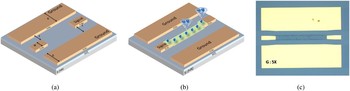
Figure 1(a) represents a coplanar waveguide (CPW), in which electrodes contacts have been fabricated by the evaporation of Ti/Au (500 Å/5000 Å) on a 1 µm silicon dioxide (SiO2) deposited by plasma-enhanced chemical vapor deposition and high resistivity silicon substrate (HRS). HRS was used, because it provides a very smooth reference surface, guarantees satisfactory RF performances, and is widely used in microwave and millimeter-wave applications due to its compatibility with the RF-integrated circuit process.
(a) CPW test structure realized onto silicon dioxide and silicon substrate (HRS), (b) inkjet printing process, and (c) microscope picture of the test structure with DWNT network.

In order to carry out the electrical characterization, a CPW test vehicle is used to host the printed layer of DWNTs. The size width (W: 90 µm) and the gap (S: 65 µm) between the signal line and the ground plane (G: 700 µm) are defined to obtain 50 Ω impedance lines. In order to fabricate a 400 µm of line length, whose width is equal or smaller than the drop diameter, a surface treatment is used. The process allows increasing the contact angle (θ), hence, confining the hydrophobic area. A contact angle of 110° is obtained by using a solution composed of 2% octadecyltrichorosilanein trichloroethylene. The next step in the deposition consists of the inkjet printing and patterning of DWNTs suspension on hydrophobic area, as shown in Fig. 1(b), in order to form the transmission line. To study the electrical parameters of the networks of DWNTs, the number of overwrites was investigated (from 1 to 17 overwrites). After deposition with 17 overwrites, the DWNT networks demonstrate a good homogeneous deposition pattern, as shown in Fig. 1(c).
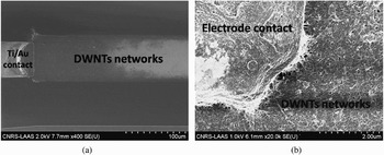
The SEM images (Figs 2(a) and 2(b)) show good contact with the electrode and line of DWNTs. After 10 overwrites, the networks are denser and fill the void unoccupied by DWNTs.
(a) SEM image of DWNT network deposited, and (b) SEM close up of DWNTs on electrode contact.

III. CHARACTERIZATION OF DWNT PATTERNS
A) DC characterization of DWNT patterns
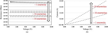
Electrical resistance of DWNTs patterns were measured at room temperature using an Agilent 4142B modular DC source controlled by a computer. The results were obtained on the test structures presented in Fig. 1 and repeated on several different samples. Different densities were characterized, started by one overwrite up to 17 overwrites. The DC results showing the variation of the electrical resistance and I–V curves are displayed in Figs 3(a) and 3(b). These curves are symmetric with respect to the applied voltage so that only the sweep over the positive range 0–10 V is illustrated.
(a) Variation graph of DWNTs networks resistance, and (b) and I–V curve of the DWNTs networks.

As mentioned above, repetitive printing makes a dense network formation of DWNTs and the resistance value of this DWNTs networks follows a reverse proportionality with respect to the number of overwrites. The resistance value decreases from 500 MΩ for single overwrite and down to 8 kΩ for 17 printing. Therefore, for an increasing density of DWNTs networks, equivalent to 10 printings, the resistance could be reduced by three orders of magnitudes. The resistivity is likely sensitive at the uniformity of DWNTs deposited, and the high resistivity value is due to poor DWNTs networks on the substrate.
From the near-zero bias results, a little non-linearity of 5% can be observed for these tested structures. This deviation can be likely associated to a tunneling mechanism phenomenon between the adjacent DWNTs. Sheng et al. [Reference Sheng15] have studied the electrical conductivity of disordered material and proposed the thermally activated voltage fluctuation across the insulating gaps as the dominating factor in determining the temperature and field dependences of the conductivity.
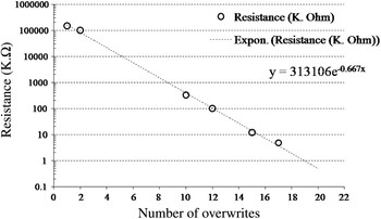
This deposition technique allows a wide range of resistance in the function of the number of overwrites. These measurement values are represented in Fig. 4. The variance resistance follows the exponential behavior because of the better percolation of the deposited DWNTs.
Variation graph of resistance versus the number of overwrites.

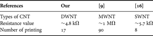
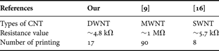
Compared to other similar works (see Table 1), an advantage of the DWNT networks presented here is the very low value of resistance attained for a much smaller number of overwrites. This can be attributed to the properties of the DWNTs which present a higher conductivity in comparison with SWNTs and the deposition technique with inkjet printing.
Summary of reported properties of CNT deposited by inkjet printing.
B) Low-frequency characterization of DWNT patterns
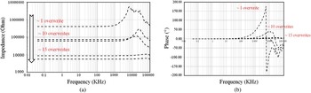
The measurements are performed with an Agilent 4294A impedance analyzer from 10 Hz to 100 MHz. The impedance and the phase dispersion curve were given in Figs 5(a) and 5(b), respectively. The measurements show a typical RLC circuit behavior. Depending on the length of the network (400 µm) and essentially on the density of DWNTs, the structures show an ohmic conductance (ϕ ≈ 0°) up to 1 MHz for 10 overwrites and over the entire considered frequency range for 15 and 17 overwrites. At higher frequencies (above 1 MHz for the 12 overwriting), the charge transport seems to be dominated by reactive (inductive and capacitive) components. At this point, the most likely explanation is that the material presents an inductive behavior caused by the interaction of single DWNTs. At lowest density (one overwrite), the inductive behavior is increased by the resonance peak at 10 MHz caused due to various reasons. Primary, the connection between different structures of nanotubes (SWNTs and DWNTs) and different properties (semiconductor or conductor) can lead to an inductive behavior. Moreover, the network of nanotubes can be considered as a network randomly oriented and connected with unoccupied and occupied area on the surface. The network is presented as some individual components. The DWNTs can form a tiny coil which would explain the inductive behavior. Kordas et al. and Song et al. described the same behavior in the function of CNT-density [Reference Kordas9–Reference Song, Kim, Yoon, Choi and Han18].
(a) Variation graph of impedance in function of frequency, and (b) and phase for different number of overwrites.

The comparison with higher-density samples shows that the overall inductive behavior due to the conducting DWNTs is masked and the ohmic transport seems to dominate. The resonance peak should be further investigated at low and high frequencies.
C) Microwave measurements
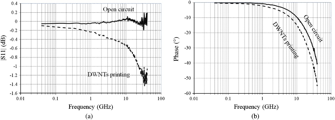
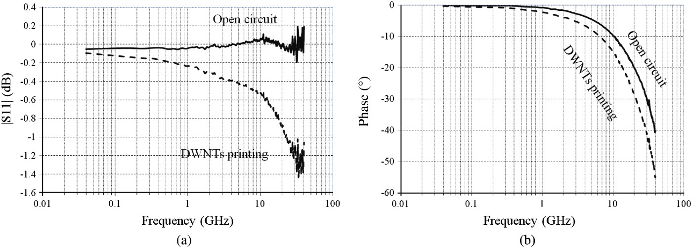
The RF behavior of these DWNT-based networks has been studied through scattering parameter measurements in the range 40 MHz to 40 GHz, by using a vector network analyzer coupled to an on-wafer probe station setup. Several test structures (as those in Fig. 1) have been characterized and the measured S-parameters showed good repeatability. The reflection data (|S 11|) of one of the test structures is plotted in Figs 6(a) and 6(b) and compared with the reference open structure. The layout of the open structure is identical to the active structure except that no DWNTs are deposited on the substrate.
S-parameters data of the DWNT network (17 overwrites) in dashed line and open circuit in continuous line measured from 0.4 to 40 GHz: (a) amplitude of |S 11| in dB, and (b) phase of |S 11| in degree.
From the measured S-parameter data, the wave propagation constant γ and characteristic impedance Z can be extracted using the theory presented in [Reference Bianco and Parodi19]. First, the devices are considered as a symmetric two-port network so that |S 11| = |S 22| and |S 21| = |S 12|, and the propagation constant is extracted using the following relationship for a lossy transmission line:

And the characteristic impedance Z can be represented as follows:
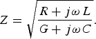
If γ and Z are known, the R, L, G, and C values can be obtained by combining (1) and (2).
R represents the series resistance per unit length; L represents the total self-inductance of the two conductors per unit length; the shunt capacitance per unit length C is due to the finite thickness of the two conductors, and the shunt conductance G models dielectric loss in the material between the conductors per unit length. These distributed transmission parameters explain the RF signal propagation constant and the impedance of characteristics in the frequency domain.
Figures 6(a) and 6(b) show the amplitude and the phase of the input reflection |S 11| data obtained from the high density of DWNT networks (17 overwrites) that measured from 0.04 to 40 GHz. In this density of DWNTs, we have said that the transmission line is essentially ohmic.
For comparison, the measurements of the open samples are also displayed. By comparing the data from the open-circuit samples, a capacitive effect caused by the very small gap between the electrodes can be noticed.
The input reflection magnitudes |S 11| of the network of DWNTs decreases from 0.15 dB at few gigahertz to less than 1.4 dB at 40 GHz, which indicates that the CNT transmit a much larger signal than the open structure.
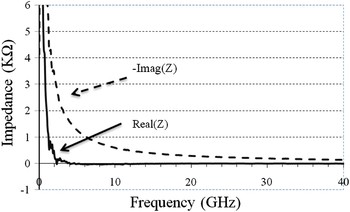
Figure 7 shows the magnitude of the real and imaginary parts of DWNTs’ line impedance as a function of frequency, obtained from the average data. The magnitude of both the real and imaginary parts decreases from 5.47 kΩ at 0.5 GHz to 1.6 Ω at 40 GHz. The imaginary part remains negative, which means RC > LG according to (2). The impedance of DWNT networks displays a capacitive character.
Real and imaginary parts of the DWNTs dynamic impedance Z with respect to the frequency from 0.04 to 40 GHz.

Note that the total contribution to the transmission is not only from the DWNT network itself, but also from the housing CPW structure. At high frequency, both the capacitance of the DWNTs and the parasitic capacitance between the IN/OUT electrodes contribute to the transmission.
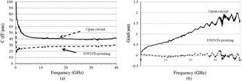
Figure 8 shows C and G values extracted as described in this section. In Fig. 8(a), the capacitance C rapidly decreases from 185 to 41 fF/µm. Figure 8(b) shows that G increases from 0.1 to 1.6 mS/µm. It is usually assumed that the dielectric loss is negligible at lower frequencies, while conductive losses prevail. One reason behind this is that the frequency-dependent shunt conductance could be associated to the substrate skin effect, where the time-varying magnetic flux penetrating into the silicon substrate leads to frequency-dependent fields.
Equivalent transmission line parameters extracted from the averaged measured data with respect to the frequency: (a) capacitance per unit length, and (b) shunt capacitance per unit length.

IV. CONCLUSIONS
In this paper, the DC and RF characteristics of DWNT networks printing by the inkjet process for potential application in the RF transmission line have been presented. The electrical characterizations highlighted a dependency of the measured resistance from the number of overwrites. Its value could be reduced from 150 MΩ to 8 kΩ from 1 to 17 overwrites, respectively.
At low frequency, we observed that the impedance was proportional to the number of overwrites and presented ohmic characteristics in wide bandwidth for high density of DWNTs. In low density, the line of DWNTs demonstrated a resonance peak at 10 MHz.
By using of S-parameters and Z measurements from 0.04 to 40 GHz, the transmission parameters (G, C) were extracted. The conductance of DWNTs networks increases significantly as the frequency increases. The capacitance decreases with increasing frequency and the dielectric loss increases. This is one of the first experimental results that support the frequency dependence of DWNT networks printed by inkjet at high frequency. Further experimental and theoretical investigations are still needed in order to well understand the transmission mechanism of DWNT networks in the microwave frequency range.
ACKNOWLEDGEMENTS
This work has been partially supported by the French National Agency (ANR) in the frame of its technological Research NANO-INNOV/RT program (NANOCOMM, project N°.ANR-09-NIRT-004) and the region Midi-Pyrénées. Moreover, we thank Norbert. Fabre and the TEAM group of LAAS-CNRS for their contribution.
 Sébastien Pacchini was born in Bastia in 1979. He received his Ph.D. degree from the CNRS/LAAS laboratory (Laboratoire d'Analyse et d'Architecture des Systèmes du Centre National de Recherche Scientifique) and the University of Paul Sabatier, Toulouse, France, in 2008. His studies have demonstrated the potentialities of carbon nanotubes into microwave applications. The work has been carried out in collaboration with the LPICM laboratory (Laboratory of the Polytechnic in Paris), CIRIMAT laboratory, and the French Space Agency (CNES) in Toulouse. He has authored or coauthored over 13 papers in refereed journals and conference proceeding. From January 2009, he has joined the Micro and Nanosystems for Wireless Communication research group in LAAS-CNRS and he is very implicate in the study of novel nanomaterial for microwave application. He works in collaboration with university, industry, and research partners in national and international projects of CNT and ferroelectric material (BST).
 Emmanuel Flahaut works as a CNRS researcher at the CIRIMAT (Inter-University Centre for Research and Engineering of Materials) at the University Paul Sabatier in Toulouse, France. He received his Ph.D. in 1999 from the University of Toulouse (catalytic chemical vapor deposition (CCVD) synthesis of carbon nanotubes (CNT) and the investigation of CNT-containing nanocomposite ceramics) and his Habilitation in 2007. He has developed a synthesis route allowing the gram-scale synthesis of double-walled CNT (DWCNT) with ca. 80% selectivity associated to a good purity. He was a post-doctoral research assistant at Oxford University in the group of Pr Malcolm Green where he worked on the filling of CNT with 1D-crystals. His main research fields are the CCVD synthesis and functionalization of CNT (DWCNT in particular), for various applications (interconnections in nanoelectronics, composite materials, sensors). In collaboration with biologists (toxicologists, ecotoxicologists), Dr. E. Flahaut is working on the human health issues related to CNT as well as the study of their environmental impact (he is leading a French program on this topic). He is author or coauthor of 106 articles in international peer-reviewed journals and has currently been advisor or co-advisor of nine Ph.D. students.
 Norbert Fabre received the engineer diploma in 1982 from the Conservatoire National des Arts et Métiers of Toulouse. He works at LAAS laboratory (Laboratory for Analysis and Architecture of Systems) of CNRS since 1971. In 2005, he was awarded by the Cristal of CNRS. He has managed the Technology Service (TEAM) of the LAAS during 20 years up to 2006. Now, his research interests are inkjet printing technology and alternatives technologies.
 Conédéra Véronique, 49ans, engineer of research, worked in the field of the hybrid circuits of 1983–1990, and integrated LAAS CNRS in 1990. She develops, on the one hand, the techniques of implementation of MEMS by Inkjet and micromachining of silicon surface, and on the other hand, the implementation of layers containing organic materials and polymers: resin moulds strong thickness, technology of sol gel, for example.
 Fabien Mesnilgrente received in 2006 a two-year diploma from a University Institute of Technology in Chemistry at the University of Paul Sabatier, Toulouse, France. Since April 2007, he has been working as an assistant engineer at the LAAS (Laboratoire d'Analyse et d'Architectures des Systèmes) specially in the TEAM department (Techniques et Equipements Appliqués à la Microélectronique). His main research interests are ink formulation, surface treatment, and inkjet printing applied to microsystems.
 Fabio Coccetti received the M.S. degree in electrical engineering from the University of Perugia, Perugia, Italy and the Ph.D. title in high frequency engineering at the Lehrstuhl für Hochfrequenztechnik at the TUM in Munich Germany, in 1999 and 2004, respectively. In 2000, he spent seven months as a visiting scientist at the Radiation Lab at University of Michigan, USA. Since September 2004, he has been working at the Laboratoire d'Analyse et d'Architectures des Systèmes (LAAS-CNRS) as a research scientist in the microsystems and nanosystems for the wireless communications group. He was hired from 2008 as R&D project manager in NOVAMEMS. His research interests include optimization of numerical techniques, multiphysics, design, and modeling of reconfigurable circuits for microwave and millimeter-wave applications with focus on RF-MEMS components. He is the member of the IEEE society, vice-chair of the MTT-S TC-25 on RF-Nanotechnology, and cofounder of the Topical Group on RF-MEMS within the European Microwave Association (EUMA).
 Mircea Dragoman was born in Bucharest, Romania, 1955. He received the M.Sc. and Ph.D. degrees from Polytechnical Institute of Bucharest, Romania in 1980 and 1991, respectively. He is a principal researcher with the National Research Institute for Microtechnology, Bucharest, Romania. He was as a visiting professor with Univ. Duisburg, Mannheim, Frankfurt, and Darmstadt, all located Germany, Tor Vergata – Rome, Italy, Univ. Saint-Etienne, and Toulouse, France. He is the author of more than 200 papers in the area of nanoelectronics, microwave and millimeter waves, terahertz, RF-MEMS, optics, and optoelectronics. He is the coauthor of the following books: Advanced Optoelectronic Devices (Springer, 1999), Optical Characterization of Solids (Springer, 2002), Quantum–Classical Analogies (Springer, 2003), and Nanoelectronics: Principles and Devices (Artech House, 2005 and 2009). His current research interests are graphene and carbon nanotube nanodevices, RF-NEMS, and terahertz electronics. He pioneers the research in the area of carbon nanotubes and graphene devices for microwave and millimeter-wave applications. I am the recipient of the 1991 Alexander von Humboldt Fellowship, and the 1999 Romanian Academy Prize “Gh. Cartianu”.
 Robert Plana was born on March 1964 In Toulouse. He received his Ph.D. in 1993 at LAAS-CNRS and Paul Sabatier University on the noise modeling and characterization of advanced microwave devices (HEMT, PHEMT, and HBT) that includes the reliability. In 1993, as an associate professor at LAAS-CNRS, he started a new research area concerning the investigation of millimeter-wave capabilities of silicon-based technologies. More precisely, he has focused on the microwave and millimeter-wave properties of SiGe devices and their capabilities for low noise circuits. In 1995, he started a new project concerning the improvement of the passives on silicon through the use of MEMS technologies. In 1999, he was involved with SiGe Semi-conductor in Ottawa where he was working on the low-power and low-noise-integrated circuits for RF applications. In the same year, he received a special award from CNRS for his work on silicon-based technologies for millimeter-wave communications. In 2000, he was a professor at Paul Sabatier University and Institut Universitaire de France and he started a research team at LAAS-CNRS in the field of microsystem and nanosystem for RF and millimeter-wave communications. His main interests are on the technology, design, modeling, test, characterization, and reliability of RF MEMS for low-noise and high-power millimeter-wave applications and the development of the MEMS IC concept for smart microsystems. He has built a network of excellence in Europe in this field “AMICOM” regrouping 25 research groups. He has authored and coauthored more than 300 international journals and conferences. In 2004, he was appointed as Deputy Director of the Information and Communication Department at the CNRS Headquarter. From January 2005 to January 2006, he was appointed director of the Information and Communication Department at CNRS. Since 2006, he is heading a research group at LAAS-CNRS in the field of microsystem and nanosystem for wireless communications. From November 2007 to November 2009, he joined the “French Research Agency” where he was the project officer of the National Nanotechnology Initiative. Since November 2009, he has been appointed as head of the department “Physic, Mathematics, Nanosciences & Nanotechnology, Information and Communication Technology” at the Ministry of research in charge of defining the French strategic for research and innovation.