I. INTRODUCTION
An increased interest in millimeter-wave (mmWave) and THz imaging for security applications has recently created a demand for integrated receiver front-ends, which can be used in phased- or focal-plane array (FPA) configurations. For imaging arrays, the number of channels or pixels present in the system is a critical factor, since it determines the resolution, unless mechanical scanning is used.
In a multi-pixel imaging system, the size, cost, and power consumption of each channel need to be optimized. Integration with the signal processing back-end electronics is also important to reduce the number of interconnects. Although III–V-based semiconductors provide more gain and lower noise at mmWave frequencies than silicon devices, Si/SiGe BiCMOS technology offers the advantage of more compact circuits with higher degree of integration. As an example, a monolithic integrated phased array has been demonstrated at 77 GHz in SiGe [Reference Babakhani, Guan, Komijani, Natarajan and Hajimiri1]. The performance disadvantage at 94 GHz with respect to III–V technologies has also been reduced with recent SiGe HBT device technology showing cut-off frequencies of 300 GHz [Reference Chevalier2] and above.
One front-end architecture capable of meeting the requirements of a monolithic multi-pixel FPA is a subharmonic mixer equipped with a low-noise amplifier (LNA) and implemented in a fully differential circuit topology. Subharmonic downconversion facilitates local-oscillator (LO) generation and distribution to multiple pixels, while the differential architecture reduces problems with cross-talk and non-constant ground potential in a multi-channel receiver. The cross-talk reduction is particularly important when antenna elements are implemented in close proximity to the receiver circuit [Reference Öjefors, Sönmez, Chartier, Schick, Rydberg and Schumacher3].
A differential implementation of an mmWave LNA in SiGe device technology has been presented at 77 GHz [Reference Chartier, Schleicher, Korndorfer, Glisic, Fischer and Schumacher4]. As transmission-line stubs were used in this design for the interstage tuning, a relatively large area was needed. However, it has been shown that spiral inductors can be used as a more compact alternative even at mmWave frequencies, with single-ended amplifier implementations available up to 140 GHz [Reference Laskin, Chevalier, Chantre, Sautreuil and Voinigescu5].
Subharmonic mixing has been demonstrated at 122 GHz in a SiGe:C process [Reference Müller, Thiel, Irion and Ruoss6]. Two cascaded mixer cores were used where the RF signal was successively multiplied by an I and Q-component of the LO signal. The die area, however, was 0.75 mm2 without pads, primarily due to the area consumption of a 90° transmission-line hybrid used to generate the necessary LO phase shift. More compact solutions, as described in this paper, are based on conventional lumped RC polyphase networks and have previously been demonstrated primarily at lower frequencies, e.g. up to 60 GHz in [Reference Svitek and Raman7–Reference Parsa and Razavi9].
In this paper we elaborate on the successful first-pass design of the compact 94-GHz subharmonic downconversion front-end previously presented in [Reference Öjefors and Pfeiffer10]. The circuit consists of an integrated LNA and subharmonic mixer and is implemented in a f max = 220 GHz SiGe HBT device technology. Lumped passive elements are used throughout the design to limit the area requirements of the front-end to 0.1 mm2 per pixel (excl. pads). Section 2 describes the proposed imaging architecture, while the circuit design of the individual blocks of the front-end is presented in Section 3. The implementation and modeling of the lumped passives are detailed in Section 4. Experimental results of the characterization of a single-ended and differential implementation of the LNA, a stand-alone mixer as well as the integrated downconverter are presented and discussed in Section 5.
II. MULTI-PIXEL IMAGING FRONT-END ARCHITECTURE
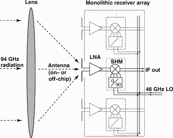
The intended multi-pixel front-end architecture is depicted in Fig. 1. In an FPA application, a lens is used to project the image of the object onto the array. Each pixel consists of an on- or off-chip antenna, an LNA, and a subharmonic mixer consisting of a modified Gilbert mixer with two cascaded switching cores. Although power- and space-consuming, the LNA in front of each mixer is needed in order to suppress the relatively high noise figure of an active mixer. In the case of zero- or near-zero-IF operation, significant front-end gain is also required to overcome the 1/f noise in the baseband or low-IF signal processing circuits.
Architecture of a subharmonic monolithic focal-plane array.

The subharmonic mixing is achieved by successive multiplication of the RF signal with the in-phase (I) and quadrature component (Q) of the LO signal in the two mixer cores and can mathematically be expressed as

which is identical to mixing of the RF signal with twice the LO frequency. Hence, this type of subharmonic mixing is not based on the use of higher-order non-linearities in the devices. The rejection of noise and unwanted signals close to the LO frequency is dependant on the phase accuracy of the generated quadrature LO signals. However, a frequency selective LNA, which provides high attenuation and low noise-output power at half of its operating frequency, is normally used in front of the subharmonic mixer. Hence, the requirements on the quadrature accuracy for suppression of the fundamental mixing products are not strict since very little signal power reaches the input port of the mixer at the LO frequency.
The subharmonic architecture has the advantage that the LO signal can be generated and distributed at half the operating frequency. By the use of a differential circuit topology, balanced on- or off-chip antennas, such as folded dipole antennas, can be connected directly to the receiver input without the need for on-chip baluns.
Another advantage of the combined use of subharmonic mixing with differential architecture is that neither the LO fundamental nor its harmonics fall into the receive band. Provided that quadrature (I/Q) mixers are used, zero-IF or near zero-IF downconversion can thus be implemented without the DC-offset or blocking problems typically caused by LO self-mixing.
The main disadvantages of the proposed subharmonic architecture over a fundamental one is the increased complexity and decreased noise and linearity performance caused by the introduction of a second mixing-quad in the mixer core. The LO power also needs to be increased in order to power the second mixing quad as well as to overcome the losses of the polyphase network.
III. CIRCUIT DESIGN
In the following sections the details of the LNA, mixer, downconverter, and integration are presented. The circuits were designed for the 0.25 µm SiGe:C BiCMOS technology (SG25H1) from IHP Microelectronics [Reference Heinemann11] featuring transistors with f max of 220 GHz.
A) Pseudo-differential 94-GHz LNA
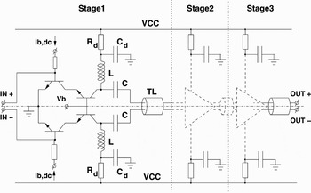
The low-noise amplifier block consists of three differential cascode stages as illustrated in Fig. 2. Although having higher noise figure than a common-emitter stage, the cascode configuration is used to guarantee that each stage provides a positive gain of 6 dB at the operating frequency of 94 GHz, which is close to half f max of the transistors. Relatively small devices (0.2 × 0.8 µm2) biased at their peak f t current density are used in the design. The use of larger transistors and emitter degeneration for simultaneous noise- and impedance-matching should however yield a minor improvement of the noise figure. Three identical stages with LC-interstage impedance matching are implemented and mirrored along the virtual ground symmetry line to form a pseudo-differential amplifier. No common-mode rejection is obtained with this amplifier architecture.
Simplified schematic of the pseudo-differential three-stage LNA. The circuit is mirrored around the virtual-ground symmetry line.

Each stage of the amplifier uses a lumped element spiral inductor L (0.3 nH) and metal–insulator–metal (MIM) capacitor C (6 fF) in an LC tank to match their output impedance to the 100 Ω differential impedance of the interstage transmission lines. With the selected device size, the input impedance as well as optimum noise-figure source resistance is close to the 100-Ω differential system impedance. Hence, the amplifier stages are not equipped with any input impedance-matching networks.
To suppress interstage cross-talk through the VCC-supply rails, a filter network consisting of the resistor Rd = 50 Ω and capacitance Cd = 80 fF is used to connect each stage to VCC. Such supply-filtering networks have been shown to yield improved isolation between on-chip building blocks and stages [Reference Sönmez, Chartier, Trasser and Schumacher12].
The simulated gain of the differential three-stage amplifier is 18 dB, with an input 1-dB compression point of −23 dBm. A relatively high noise figure of 11.3 dB is obtained in the simulation due to the use of small devices. Incorporation in the simulation of an optimum-noise impedance-matching network at the amplifier input yielded noise-figure improvements of less than 1 dB and was thus omitted. By the use of a state-of-the-art device technology and an optimized low-noise design, it is expected that a noise figure less than 7 dB could be obtained.
The three-stage cascode amplifier draws 11 mA from a 3.3-V supply. To simplify design and testing, each stage of the LNA uses separate current mirrors, which increases the total current consumption of the LNA to 28 mA. However, by the use of an optimized and shared biasing network, the total current consumption can be reduced to less than 15 mA.
B) Subharmonic mixer
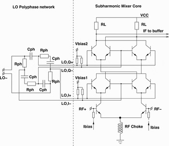
The subharmonic mixer, shown in Fig. 3, is based on a Gilbert mixer with two cascaded switching quads, each fed with the LO 90° out-of-phase through the help of an RC polyphase network.
Schematic of the subharmonic mixer and polyphase network. Biasing and the output buffer is excluded.

A conventional RC polyphase filter is used to generate the required LO and LO signals at the LO frequency of 46 GHz. Although lossy, the lumped element polyphase network is significantly more compact than the 90° hybrid used in [Reference Müller, Thiel, Irion and Ruoss6]. In the simulation, 8 dBm LO drive power is required for maximum conversion gain. Most of the LO power is consumed by the 50-Ω resistors in the polyphase network. A higher impedance network can be implemented in order to reduce the necessary LO drive power for the required voltage swing at the mixer-quad bases. Increased impedance of the polyphase network would however make wide-band quadrature generation and impedance matching more difficult as the network becomes sensitive to loading effects. The losses in the LO path can also be reduced by the use of a lumped LC network for the quadrature generation. A suitable quadrature all-pass filter implementation [Reference Koh and Rebeiz13] would require an on-chip area of 0.4 mm.
A broadband IF bandwidth of up to 10 GHz was achieved by using 200-Ω load resistors and a differential emitter follower buffer. The simulated conversion gain and 1-dB input compression point were 5 and −8 dBm, respectively. If desired, a higher conversion gain over a reduced IF bandwidth may be obtained by the use of larger collector load resistors or a tuned output network.
To enable 3.3-V operation of the mixer, despite the use of three stacked transistors and resistive collector loads, the tail current source in the RF stage of the mixer was replaced by a spiral inductor. This inductor acts as an RF choke and improves the rejection of common-mode signal components by the mixer. The total current consumption of the mixer is 17 mA, of which the majority is consumed by the common-emitter IF output buffer. This buffer is only required to drive the external measurement equipment in a 50-Ω characterization environment. Less than 7 mA from a 3.3-V supply is required to power the mixer core.
IV. LAYOUT AND PASSIVES
The inductors and transmission lines were designed for the five-layer aluminum back-end provided by the IHP SG25H1 process technology [Reference Heinemann11].
A) LNA tank spiral inductors
The implementation of the lumped inductances in the LNA tank network is critical since modeling errors can lead to significant de-tuning of the LNA. Spiral inductors in silicon technology have traditionally been considered as lossy and difficult to model due to the interaction with the substrate. However, at mmWave frequencies the substrate coupling is reduced by the small inductor area required as well as the availability of a thick back-end oxide in modern process technology. Here, a stacked metal layer design with the inductor turns in multiple layers [Reference Gordon, Yao and Voinigescu14] is used to further minimize the area requirements and substrate coupling.
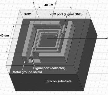
In Fig. 4 the stacked two-and-a-half-turn LNA tank inductor is depicted. It is implemented as separate square turns in the two topmost metal layers of the back-end. Each turn has a 25 µm side length and is connected to the other turn by a via contact. The inductor provides an equivalent of 0.25 nH inductance to signal ground (VCC) at 94 GHz. To minimize parasitic coupling to other parts of the circuit, the spiral inductor is enclosed by a grounded metal shield wall equipped with substrate contacts. Although the inductance, and hence also the quality factor, is reduced by induced currents in the metal shield walls, the use of side shields has been shown to yield up to 20 dB increased isolation between adjacent inductors [Reference Mikkelsen, Jensen and Larsen15].
HFSS 3D EM-model of LNA tank spiral inductor with turns stacked in two metal layers.

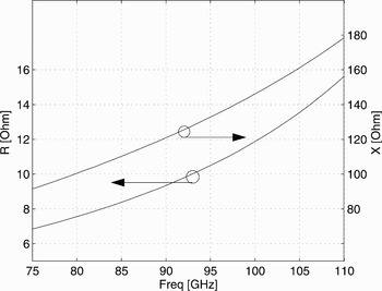
The tank inductor has been designed and modeled using the EM-simulation tool HFSS. The simulation results are presented in Fig. 5 for the 75–110 GHz frequency range.
HFSS simulation of inductor resistance R and reactance X at the collector node of the tank circuit with the other port connected to the decoupled VCC signal ground.

At 94 GHz the simulated quality factor is 12. A strong frequency dependence of the losses is caused by the 140-GHz self-resonance of the inductor. For circuit design purposes, a simple one-port model (VCC port ac-grounded) was fitted to the S-parameters obtained through the EM simulations. The model consists of an inductance L = 0.15 nH, series resistance Rs = 5 Ohm, and parallel capacitance Cp = 6 fF to ground. Over the 75–110 GHz frequency range of interest for the LNA design, this model provides good agreement with the EM-simulation results.
B) Shielded transmission lines
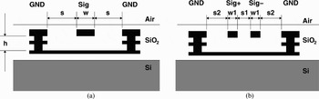
Although lumped inductors are used in the impedance-matching circuits, low-loss transmission lines with well-defined impedances are required for the interstage signal paths as well as on-chip routing to the pads. In Fig. 6(a) a shielded microstrip line based on previous implementations [Reference Goren16] of transmission lines in silicon process back-ends is shown. The signal conductor is drawn in the top interconnect metal layer available in the back-end, while the ground plane is implemented in a deeper metal layer, thus fully shielding the signal line from the lossy silicon substrate. Side ground shields, formed by stacked vias and conductor stripes, provide confinement of the fields generated by the microstrip line and limit coupling to adjacent circuits.
(a) Shielded microstrip transmission line Si/SiGe BiCMOS process backend. (b) Differential coplanar stripline (CPS)/coupled-microstrip version of the same transmission line used for interstage signal paths.

Microstrip transmission lines with 50 Ω line are realized with a signal conductor width of w = 8 µm, distance to side shields s = 11 µm, and dielectric thickness h = 6 µm. At 94 GHz, the measured de-embedded loss of this single-ended line was 0.87 dB/mm with an effective dielectric constant of ɛ r = 3.25. The loss figures show reasonable agreement with published values for similar process technologies [Reference Zwick, Tretiakov and Goren17].
For the differential interstage signal a differential transmission line (Fig. 6(b)) has been derived from a shielded microstrip line. It provides a hybrid CPS and microstrip mode with a 100 Ω odd-mode (differential) impedance and 51 Ω even-mode (common mode) impedance. As no characterization data are available for this line, HFSS simulations were used for the design yielding a signal conductor width w1 = 2 µm, gap s1 = 4 µm, and side shield distance s2 = 8 µm. The simulated loss at 94 GHz of the differential transmission line is 1.25 dB/mm and the effective dielectric constant is equal to 3.9.
C) Baluns and test sites
In the intended application, the differential front-end circuits are interfaced directly to a balanced (dipole) antenna, which can reside either on- or off-chip. Test sites with baluns at the RF and LO ports were designed (Fig. 7) to facilitate characterization in a single-ended wafer probing environment.
Test site with on-chip baluns for characterization in a single-ended wafer-probe environment of the integrated downconverter.

The baluns were implemented as tuned transformers with windings in adjacent metal layers. The 94-GHz balun layout consists of one square turn for each port interleaved with the other winding, while the 46-GHz balun is equipped with two interleaved turns per winding. Both baluns feature 2-µm line width and inter-line spacing as well as outside dimensions of 50 × 50 µm. The associated losses of the RF balun were extracted from back-to-back test structures and found to be 3.5 dB.
In addition to the differential circuits, a single-ended version of the pseudo-differential LNA was implemented by dividing the circuit in half. This break-out circuit was used in order to be able to characterize the LNA without the inaccuracies of the on-chip baluns.
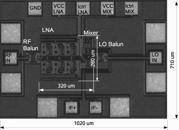
A micrograph of the single-channel downconverter test site is shown in Fig. 8. Similar test sites were provided for the LNA and subharmonic mixer, respectively.
Downconverter micrograph with auxiliary 94-GHz RF test-balun (left), LNA, mixer, and 46 GHz auxiliary LO test-balun (right). The size of the downconverter core is 320 × 260 µm2.

V. CHARACTERIZATION RESULTS
The LNA and subharmonic mixer circuits have been characterized individually well as in the intended integrated configuration.
A) LNA characterization
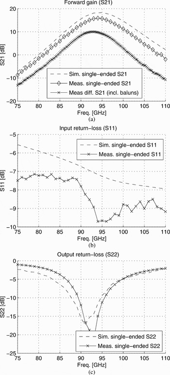
The measured small-signal gain as well as input and output return loss is shown in Fig. 9 together with the simulation results. A maximum gain of 16 dB (simulated 18 dB) is obtained at 94 GHz. Since the input of the LNA is not impedance matched, a relatively high return-loss (S11) level of −9 dBm is measured.
Measured and simulated gain (a), input return-loss (b), and output return-loss (c) of the single-ended version of the LNA. The measured gain of the pseudo-differential LNA including balun losses at the input and output is included in (a).

The measured differential amplifier gain is 10 dB including the losses of the input and output balun (2 × 3.5 dB) and is hence in agreement with the single-ended LNA results.
No noise figure measurements were performed due to the non-availability of a suitable calibrated noise-measurement setup.
B) Mixer characterization
The simulated and measured mixer conversion gain is shown in Fig. 10 versus the 46-GHz LO-drive level at the input of the polyphase network. The measurement used a −25 dBm RF input signal at 94 GHz.
Measured (circles) and harmonic balance (HB) simulation (line) mixer conversion gain as a function of LO power. RF input level −25 dBm.

The available power at the input to the polyphase network was estimated from the LO generator power, cable losses, and LO test-balun losses. Sufficient power was not available during the characterization to obtain maximum conversion gain, due to an 8-dB insertion loss in the cables and the auxiliary LO test balun. Hence, the conversion gain was limited to 3 dB, which is in agreement with simulations for this LO drive level.
C) Downconverter characterization
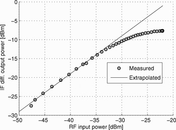
The downconverter has been evaluated using the test circuit shown in Fig. 7 and 0-dBm LO drive power. Figure 11 presents the 2-GHz output power versus the 94-GHz input power.
Measured differential IF output signal as a function of the 94-GHz RF input power to the downconverter with an estimated 46-GHz LO level of 0 dBm at the input of the polyphase network.

A small-signal conversion gain of 20 dB is obtained at 94 GHz, which corresponds to the measured 17-dB gain of the LNA and 3-dB conversion gain of the mixer. The 1-dB compression point is reached at an input level of −31 dBm.
The system noise figure was calculated from the mixer conversion gain G, and the quiescent input (N 0) and output (P 0) noise spectral densities were calculated as follows:

where N 0 is −174 dBm/Hz and P 0 = −137 dBm/Hz for a 2-GHz IF signal, respectively. All noise spectral densities were measured with a spectrum analyzer. With a measured conversion gain of G = 20 dB, the single-side-band (SSB) system noise figure is 17 dB. The measured output noise level was however close to the noise floor of the available spectrum analyzer, which can cause an overestimation of the system noise. The anticipated error is up to 3 dB. Based on the 11.3-dB simulated noise figure of the LNA the expected SSB cascaded system noise figure for a low-IF system (where the mirror frequency falls within the LNA bandwidth) should be close to 15 dB, thus corresponding to a 12 dB DSB noise figure in a zero-IF (with an additional quadrature mixer core) or high-IF superheterodyne configuration.
VI. CONCLUSION
A subharmonic monolithic downconverter with 20-dB conversion gain at 94 GHz has been implemented in the SiGe:C process technology. The full down converter requires a die area of only 0.1 mm2 (excluding pads), due to the use of lumped passive elements, and is hence suitable for compact highly integrated multi-pixel imaging front-ends. Although the system noise figure of the implemented circuit is high compared to III–V downconverters, enhancements by the use of state-of-the-art SiGe device technology as well as an improved LNA design is anticipated to significantly reduce the noise figure. The presented front-end architecture is suitable for zero-IF and broad-band operation (if extended with quadrature down-conversion) due to its large IF bandwidth and the absence of significant LO-self-mixing.
ACKNOWLEDGEMENT
This work was partly supported by the European Commission through the European Young Investigator Award.
 Erik Öjefors received his M.Sc. degree in engineering physics and his Ph.D. degree in microwave technology from Uppsala University, Sweden, in 2000 and 2006, respectively. In 2007 he joined the Institute of High-Frequency and Quantum Electronics at the University of Siegen, Germany. Since 2008, he is with the Institute for High-frequency and Communication Technology at the University of Wuppertal, Germany. He was the co-recipient of the 2007 IEEE AP-S R.W.P. King Award and the 2008 EuMIC Best Paper Award.
 Johannes Borngräber was born in Frankfurt (Oder), Germany, in 1955. He received his M.Sc. degree in mathematics from the Humboldt University in Berlin in 1981. Since 1983, he has been with Innovations for High Performance Microelectronics (IHP), Frankfurt (Oder), Germany. He worked in the Electron Beam Lithography group and in the circuit design team. Now he is responsible for measurement of integrated microwave and millimeter-wave circuits.
 Falk Korndörfer was born in Plauen, Germany, in 1975. He received the diploma degree from the Chemnitz University of Technology, Chemnitz, Germany, in 2002. He was a Research Scientist with the Chemnitz University of Technology until the end of 2003. Since 2004, he has been with Innovations for High Performance Microelectronics (IHP), Frankfurt (Oder), Germany, where he is responsible for characterization and measurement of integrated microwave and millimeter-wave devices and circuits, and for the modeling of passive MMIC elements.
 Ullrich R. Pfeiffer received the diploma degree in physics and the Ph.D. in physics from the University of Heidelberg, Germany, in 1996 and 1999, respectively. In 1997 he worked as a research fellow at the Rutherford Appleton Laboratory, Oxfordshire England. In 2000 his research was based on real-time electronics for a particle physics experiment at the European Organization for Nuclear Research (CERN), Switzerland. From 2001 to 2006 he was with the IBM T.J. Watson Research Center where his research involved RF circuit design, power amplifier design at 60 and 77 GHz, high-frequency modeling and packaging for millimeter-wave communication systems. In 2007 he received a European Young Investigator Award and led the THz electronics group at the Institute of High-Frequency and Quantum Electronics at the University of Siegen, Germany. Since 2008 he holds the High-frequency and Communication Technology chair at the University of Wuppertal, Germany. Dr. Pfeiffer is a member of the German Physical Society (DPG). He was the co-recipient of the 2004 and 2006 Lewis Winner Award for Outstanding Paper at the IEEE International Solid-State Circuit Conference, the co-recipient of the 2006 IBM Pat Goldberg Memorial Best Paper Award, and the 2008 EuMIC Best Paper Award.