I. INTRODUCTION
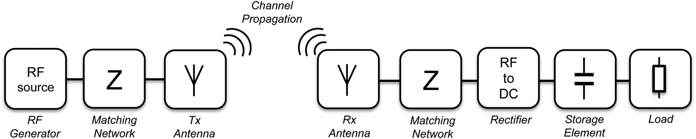
Today's society is evolving toward creating smart environments where a multitude of sensors and devices are interacting to deliver an abundance of useful information. Essential to the implementation of this Internet of things (IOT) is the design of energy efficient solutions aiming toward a low-carbon emission, namely green, society. Within this context, the energy harvesting appears as an alternative to provide systems with self-sustained operation. Many electronic devices operate in conditions where it is costly, inconvenient, or impossible to replace the battery. Examples include sensors for health monitoring of patients [Reference Paing1, Reference Bernhard, Hietpas, George, Kuchima and Reis2], aircraft or building structural monitoring [Reference Walsh, Rondineau, Jankovic, Zhao and Popovic3, Reference Zhao4], sensors in natural, industrial or hazardous environments, etc. The scavenging of natural ambient energy requires some specific conditions such as: daylight for solar energy [Reference Lin5], breeze for wind energy or motion for kinetic energy [Reference Paradiso and Starner6] to name a few. As consequences the exploitation of natural source does not fit with many cases of applications. On the other hand, the electromagnetic (EM) [Reference Foster7], or radio-frequency (RF), energy is a human-made source that is not dependent of weather conditions nor the daytime. It is so very attractive for wireless powering of remote devices. Furthermore, the ever growing commercial and personal wireless installations opens up to a 24 h a day available energy in the vicinity of any human activity areas. The schematic of a general wireless RF power transmission (WPT) system is shown in Fig. 1. We talk here about far-field RF energy transmission [Reference Le, Mayaram and Fiez8], which is different from near-field RF energy transmission [Reference Hirai, Kim and Kawamura9]. This later including inductive, capacitive, or resonant coupling is a close contact transmission and is not relevant for remote devices. In Fig. 1, the receiver antenna collects the EM energy radiated by an RF source, and converts it into an RF signal. This RF signal is transferred to the rectifier by an impedance matching network, to be converted into DC power, which is further accumulated in a storage element. The main purpose in the deployment of WPT systems is the development of compact and efficient solutions. Most of the challenges concern the implementation of harvesting modules, especially the antenna as its design defines the scavenging capability and the size of the RF harvester. At low frequency the transfer of energy is efficient, but the antenna footprint is large. To address the trade-off between the efficiency of the WPT and the size of the modules, the frequency band located in the 433 MHz–6 GHz frequency spectrums are preferred.
Schematic of a wireless RF power transmission (WPT) system.

Over the last decade the research effort has focused on the development of WPT systems according two scenarios: the RF energy scavenging [Reference Nishimoto, Kawahara and Asami10] and the RF energy transfer [Reference Shinohara11]. The two RF energy scavenging is an opportunistic collection of the RF ambient energy from the surrounding communication traffic. To improve the harvesting capability the scavenging RF harvesters are of wide-band type [Reference Pinuela, Mitcheson and Lucyszyn12] and cover popular standards such as: digital television (DTV) (470–610 MHz), global system for mobile communication (GSM) 900, GSM1800, third-generation cell-phone technology (3G) (2.1 GHz), and WiFi (2.4 GHz). Unfortunately these standards dedicated to convey wireless communications do not radiate a large RF power. As consequences the collected energy is weak, unpredictable, and out of control. The RF energy scavenging remains a promising solution in the future as the increase of communication traffic could make it more reliable, and consistent with IOT applications. The second concept, namely RF energy transfer, assumes an identified source that is dedicated to perform the WPT. The amount of transmitted power is controlled by the source and the collected energy is larger than in the scavenging approach. The licence-free industry–science–medical (ISM) frequency bands located at 0.9, 2.4, and 5.8 GHz are usually exploited to support such a WPT scenario. Today the RF energy transfer in ISM bands is not only promising, it becomes a reality as some pioneer companies propose some full kits: Powercast Corporation, AnSem, and MicroChip to name a few. However, there is still a lot of work to make the RF energy transfer an appropriate, low cost, and easy-to-use solution for remote powering. One of the most critical point concerns the harvesting capability of the RF modules. So far the commercial kits referenced above only explore the 900 MHz ISM allocations to perform the WPT. This work proposes to demonstrate the interest of a concurrent harvesting at 915 MHz and 2.44 GHz. The design and implementation of a modified four-stage doubler RF-to-DC converter, including a concurrent matching network, is first presented. Section III details the design of two types of multi-band antenna. The comparison between a single frequency and a multi-band WPT is exposed and the demonstration of the remote powering of a clock is reported as a case of application. To conclude a comparison of our results with the state of the art is exposed.
II. CONCURRENT RF-TO-DC CONVERTER
The RF identification (RFID) applications are the most popular systems exploiting the principle of RF energy transport. In passive RFID applications, the reader transmits the RF power to the tag, and also sets up the communication. The RF-to-DC converter is designed to yield a maximum of power efficiency to the tag. Most of the time the reader and the tag are in line of sight and close to each other, these conditions improve the transmission of RF energy, the amount of power available at the tag antenna is large, typically between −15 and −20 dBm. In RF, the energy harvesting scenario is different. The distance between the RF source and the RF harvester ranges from 0.5 to 10 m. The amount of collectable power is low, from −10 to −25 dBm, and the remote powering is difficult. The RF harvesters are supposed to collect and to store the energy during a long period of time. Once the level of stored energy is large enough, it can be released to the application. For these reasons a rectifier dedicated to RF energy harvesting is first designed to yield a maximum of sensitive to increase its scavenging time and capability.
A) Rectifier architecture
The rectifier architecture is based on voltage multipliers to provide an adequate output DC voltage. The architecture of the RF-to-DC converter, reported in Fig. 2, includes a matching network based on an L-section, and an N-stage voltage multiplier based on Schottky diodes from Avago (surface zero bias schottky detector diodes (HSMS)285). The choice of the Schottky diode is very important in the design of the rectifier. A key parameter is its threshold voltage V TH. When only low power levels are available in the environment, the amplitude of the incident signal may be close to or even below this voltage. Below this voltage value, the diode will no longer conduct and the losses become predominant. For commercially off-the-shelf (COTS) devices the two Schottky diodes performing the best conversion efficiency in a 2.4 GHz range are HSMS-2850 from Avago and SMS-7630 from Skyworks [Reference Hemour and Wu13].
Architecture of the RF-to-DC converter.
Focusing on the sensitivity, the RF-to-DC converter is designed to maximize the rectified voltage for an input power close to −20 dBm. The optimum number of stage is fixed to four according [Reference Taris, Fadel, Oyhenart and Vigneras14]. The footprint of each voltage doubler imposes the micro-strip line network. The micro-strip lines namely “junction” is set to minimum length, the micro-strip lines “access” are used as an additional degree to tune the input-matching network. Indeed, the L section in combination with the micro-strip distributed network is equivalent to a T section (Fig. 3). Many combinations of Z 1, Z 2, and Z 3 can achieve input matching at 900 MHz or 2.4 GHz. Some of them are very close for each frequency, so we choose one that allows a return loss (< −10 dB at least) both at 900 MHz and 2.4 GHz.
Topology of the input-matching network.
The equivalent narrow band model of the matching network is proposed for each frequency (Fig. 4). At 915 MHz, the voltage multiplier, including the rectification stages and the micro-strip line network, is modeled with a shunt capacitor (5 pF) and a shunt resistor of 270 Ω (Fig. 4(a)). The stub (Fig. 3) is equivalent to an inductor (Fig. 4(a)), which compensates the shunt capacitor. The input micro-strip line, (Fig. 3), is a quarter wave impedance transformer, (Fig. 4(a)) it converts the 270 Ω into 50 Ω. At 2.44 GHz the micro-strip line network distributing the RF signal to the voltage doublers (Fig. 3), becomes inductive (Fig. 4(b). The stub is equivalent to a shunt capacitor of 120 fF, its effect is negligible. The impedance transformation is actually performed by the input micro-strip line, which is modeled by a shunt capacitor (0,6 pF) and a series inductor of 5.6 nH.
Equivalent model of the RF-to-DC converter, 915 MHz (a), 2.44 GHz (b).
To study the impact of the power on the diode, and input matching behavior the return loss of the four-stage rectifier has been measured and plotted (Fig. 5) for various input power P rf at 9000 MHz.
Measured S 11 of a four-stage voltage multiplier with a L section at 900 MHz for various input power P rf.
As illustrated in Fig. 5, the input return loss is not strongly affected by the input power if P rf < −15 dBm. The RF harvesters developed in this work are dedicated to collect power from −15 to −25 dBm. Over this range the diode model can be considered as stable, and the slight frequency shift is still covered by the antenna bandwidth.
B) Rectifier characterization
The power efficiency and the power sensitivity are two conversion characteristics of importance in RF harvesters. However, the RF harvester operating at the low-power level accumulates the energy in a storage element, to further release it to the application. In such accumulation mode, the power sensitivity becomes more important than the power efficiency.
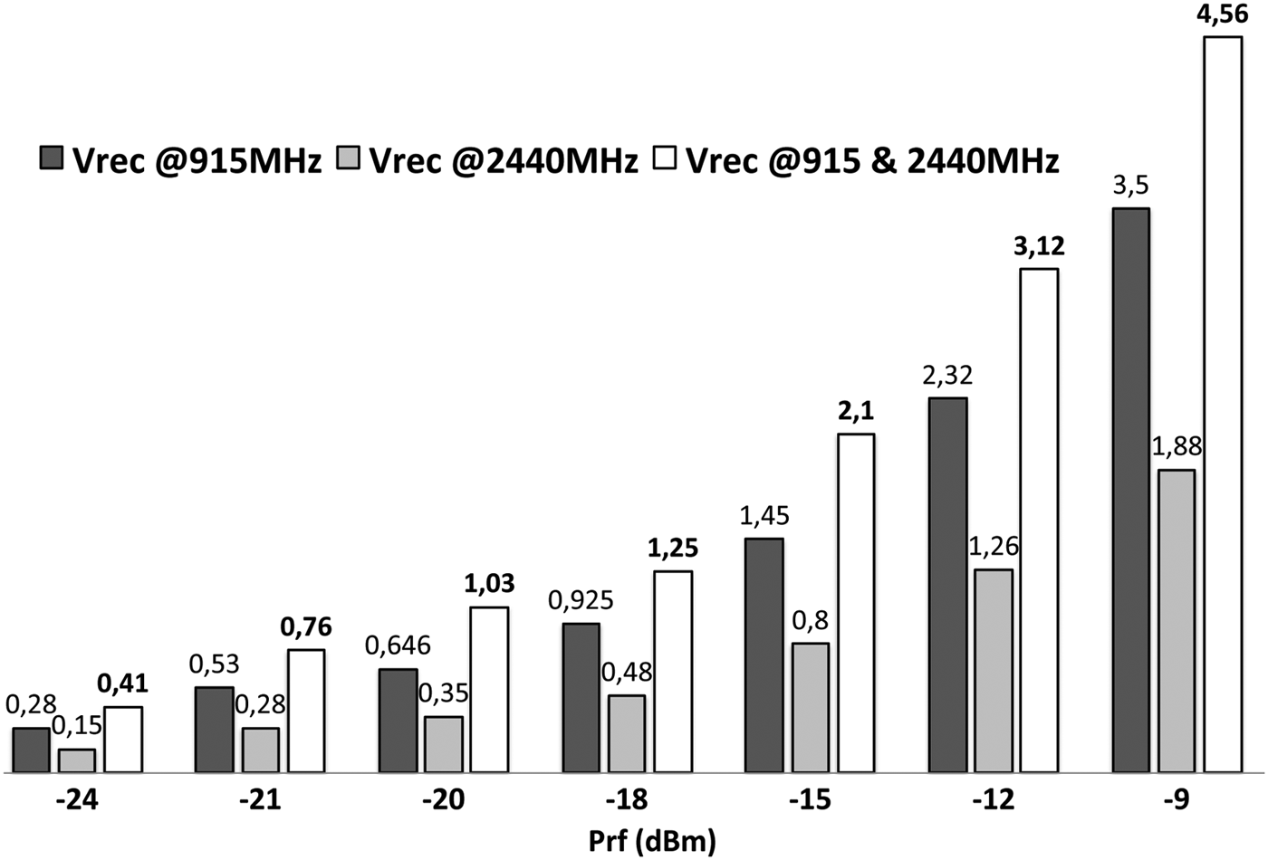
For the characterization the rectifier is not connected to a load. The load represents the equivalent impedance of the application (clock, sensor) to power. The effectiveness of RF–DC conversion of the rectenna and its DC ouput voltage varies depending on the load value. The rectifier is first characterized in a single tone mode, 915 MHz and 2.44 GHz, respectively, and then in a dual-band mode. Measurements of the unloaded rectified voltage versus various input power P rf are reported in Fig. 6.
Unloaded rectified voltage for various inpout power.
To compare the results of the two considered tones, the target is fixed to a value of 1 V. In a single tone mode, the required P rf to rectify 1 V is close to −18 dBm at 915 MHz, and would be larger than −15 dBm at 2.44 GHz. In a dual-band mode, the circuit only needs a power P rf of −20 dBm at each frequency. The dual-band rectification significantly improves the power sensitivity. The reverse breakdown voltage of the HSMS285 Schottky diode limits the input power to −9 dBm, for which V rec is 4.56 V.
III. ANTENNA DESIGN
To meet the low-cost constraints, the RF energy harvester will be implemented on a single low-cost substrate, an FR4 printed circuit board (PCB). For the antenna, there are more efficient substrates with a higher permittivity to reduce the size of the antenna or a lower losses but their cost is much higher than the improved performance. These powerful substrates fail to build low-cost energy harvesters. This section exposes the design of two dual-band antennas implemented on a 1.6 mm FR4 printed circuit board. The fabrication uses a mechanical etching process with a 200 µm resolution. We have chosen two complementary antenna topologies with a directional and omnidirectional radiation pattern.
A) Dual-band patch antenna
Emitting and receiving antennas do not usually meet the same constraints. Mobile devices such as smartphones and tablets use compact antennas (ifa, pifa, etc.) to address the trade-off between performance and size. Base stations can afford large efficient radiating elements (omnidirectional or directional antennas depending on the application). For energy harvesting purpose, micro-strip patch antennas are commonly used [Reference Shrestha, Noh and Choi15–Reference Hasan and Giri17]. A rectangular micro-strip patch antenna (RMPA) is first developed to suit with both low-cost technology of implementation and co-integration with the rectifier. Based on the cavity-model approximation, the resonant frequencies of the RMPA for the TMmn mode is described in (1).
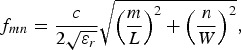 $${f_{mn}} = \displaystyle{c \over {2\sqrt {{\varepsilon _r}}}} \sqrt {{{\left( {\displaystyle{m \over L}} \right)}^2} + {{\left( {\displaystyle{n \over W}} \right)}^2}}, $$
where W and L are the patch dimensions, c = 3.108 m/s.
The antenna dimensions, 68 cm2 (8.8 × 7.8 cm2), as described in Fig. 7(a) are dependent to the frequency bands and the feed location is selected to only excite the fundamental modes TM01 and TM10. Those modes permit to obtain a large aspect ratio (W/L = 2,7) but reduce the performance of the RMPA. On the other hand, TM01 and TM30 modes require an aspect ratio close to one but offer beneficial radiation patterns for our application. The RMPA is fed by a probe whose position (x,y) adjusts the matching both at 915 MHz and 2.44 GHz. This two operating bands of the proposed antenna are on cross-polarization planes. The geometric parameters of RMPA have been optimized with an approximate model, the transmission line (TL) model [Reference Visser18], and with a full wave method. Details of the two approaches have been studied in [Reference Berges, Fadel, Oyhenart, Vigneras and Taris19]. The return loss of the RMPA is better at 915 MHz than 2.44 GHz because the maximum impedance of TM30 mode is 31 Ω [Reference Berges, Fadel, Oyhenart, Vigneras and Taris19]. The TM30 mode does not achieve 50 Ω because it is not a fundamental mode. This antenna has a maximum gain of 1.3 dB at 915 MHz (Fig. 7(b)) and 2.5 dB at 2.44 GHz (Fig. 7(c)). This two operating bands of the proposed antenna are on cross-polarization planes.
Layout of the RMPA antenna (a), radiation pattern at 915 MHz (b) and at 2.44 GHz (c). Solid and dashed lines correspond to the E- and H-planes, respectively.
The realized gains of the dual-band patch antenna are lower than the classical patch antenna because the radiating efficiency is low, 60% for the TM01 mode and 30% for the TM30 mode. The FR4 substrate has a loss tangent of 0.02. The radiation efficiency of the dual-band patch antenna is highly dependent of the substrate losses.
B) Multi-band arm dipole antenna
The second antenna is a multi-band dipole type composed of three arms. Its dimension is about 23 cm2 (11.1 × 2.1 cm2), Fig. 8(a). Each arm is designed to work at one band of frequency. The longer one is for the 915 MHz, the middle one, not useful in our case, is for the 1.4 GHz, and the last one, the smaller, is dedicated to 2.4 GHz [Reference Lu, Guo and Huang20].
Layout of the multi-band arms dipole antenna (a), radiation pattern at 915 MHz (b), and at 2.44 GHz (c). Solid and dashed lines correspond to the E- and H-planes, respectively.
All the geometric parameters have been optimized with a full-wave method in order to be matched both at 915/ 2440 MHz. On Fig. 6(b) and 6(c), the radiation pattern is plotted for the elevation plane (orthogonal to substrate) of the simulated antenna. The maximum gain is 0.5 dB at 915 MHz and 3.4 dB at 2.44 GHz at 90°, on the substrate plane. The radiation efficiency is 99% at 915 MHz and 95% at 2.44 GHz.
It is interesting to compare the characteristics and performances of the two types of antennas. Although the radiation efficiency of the dipole antenna is better than the patch antenna, the antenna gains are similar because the high directivity of the RMPA antenna compensates the low values of radiation efficiency. When there are no cost constraints, it is interesting to use high-performance substrates for the design of RMPA antennas because they improve the radiation efficiency and consequently antenna gain.
Moreover, the integration of the antenna with the rectifier will not be made in the same way. Considering the patch antenna, the rectifier can be integrated on the ground plane allowing a more compact solution. The dipole antenna, which is ground plane free, is less sensitive to the surrounding environment in our case. The performance of the dipole antenna and especially the radiation efficiency are very weakly dependent of the substrate characteristics. The design of a dipole antenna can be easily reused with other material such as Kapton®, paper, Plexiglas to name a few.
IV. WIRELESS POWER TRANSMISSION
This part presents the measurement results of the assembled RF harvesters in the context of wireless power transfer. The two dual-band harvesters are realized with COTS devices such as HSMS diodes and capacitors. Those elements are reported by heat treating. The RF-to-DC converter board, including the matching network and the rectifier, is reported on the backside and connected to the radiation part, on the front side, through a via (Fig. 9(a)). The dipole antenna is connected to the rectifier circuit using SMA connector (Fig. 9(b)).
Dual-band RF harvesters based on patch antenna (a) and arms dipole antenna (b).
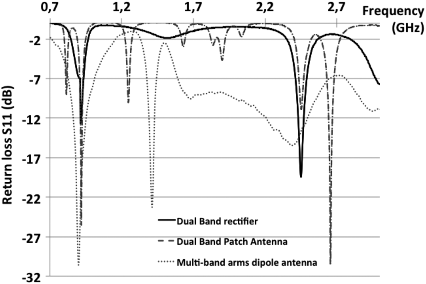
For the dual-band RF harvester based on patch antenna, the return loss, S 11, is measured for an input power of −20 dBm with a HP8720 network analyzer. The patch antenna, the rectifier and the dipole antenna are centered at 915 MHz and 2.44 GHz with a low return loss (S11 < −15 dB), Fig. 10. The return loss of the RMPA antenna is better at 915 MHz than 2.44 GHz because the maximum impedance of TM30 mode is 31 Ω (Figs 6 and 7 of [Reference Sim, Shuttleworth, Alexander and Grieve16]). The TM30 mode does not achieve 50 Ω because it is not a fundamental mode.
Measured return loss S 11 of the dual-band rectifier, patch, and arms dipole antenna.
A) Remote powering and power efficiency
The rectenna is connected to a clock, which mimics a low power application. The remote powering of this clock is performed in a furnished room of the lab according the schematic of Fig. 11. The distance between the source and the antenna is fixed to 2 m. The clock is turned on for different scenarios of transmitted power. For each combination of power proposed in Fig. 12, the RF power is first measured with a calibrated antenna and a power meter. Then, the rectenna is measured and P eff is the ration between the power delivered to the load (here the clock) and the power available at the antenna.
Schematic and picture of the scene of remote powering of a clock.
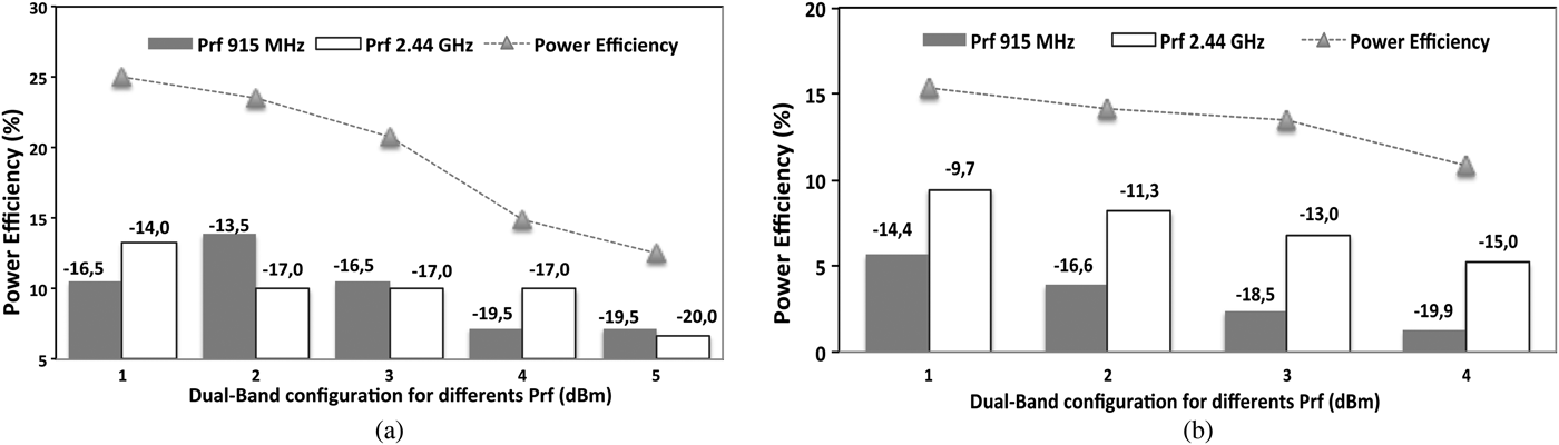
Power efficiency of the dual-band RF harvester based on the patch (a) and the arms dipole (b) antenna.
The power efficiency of the patch and the dipole rectenna is worked out from these experiments and reported in Fig. 12. The power efficiency η is defined as the ratio between the DC power delivered to the clock and the RF power collected by the antenna.
The minimum power required to turn on the clock with the patch-based harvester, Fig. 10(a), is a two-tone signal featuring: −19.5 dBm at 915 MHz and −20 dBm at 2.44 GHz. At this point, the power efficiency is 12.5%, which corresponds to a DC output power of 2.7 µW/1 V.
A maximum efficiency of 24% occurs for a combined power of −16.5 dBm at 915 MHz and −14 dBm at 2.44 GHz. The harvester is able to deliver a DC ouput power of 15 µW. The harvester based on the arm dipole antenna needs a minimum power of −19.9 dBm at 915 MHz and −15 dBm at 2.44 GHz at the antenna to turn on the clock. For these conditions of remote powering, the efficiency of the harvester is 11%. It delivers a DC power of 3.8 µW/1.15 V. The maximum power efficiency, 15.5%, yields for an input power of −14.4 dBm at 915 MHz and −9.7 dBm at 2.44 GHz, the DC output power is 21 µW.
This scenario of remote powering figures out that the harvester based on the patch antenna exhibits a better power efficiency than the harvester combined with the dipole element. This difference is due to the antenna gains. Referring to Figs 7 and 8, the gain of the patch antenna is larger (+0.8 dB) at 915 MHz and lower (−0.9 dB) at 2.44 GHz than the dipole element. However, the rectifier, referenced in [Reference Sim, Shuttleworth, Alexander and Grieve16], achieves a power efficiency of 17% at 915 MHz and only 5% at 2.44 GHz for an input signal of −15 dBm. As consequences the patch-based harvester is able to extract more power from a 915 MHz signal than the dipole-based harvester can do at 2.44 GHz. For this reason the overall efficiency of the patch harvester is better.
B) Power sensitivity
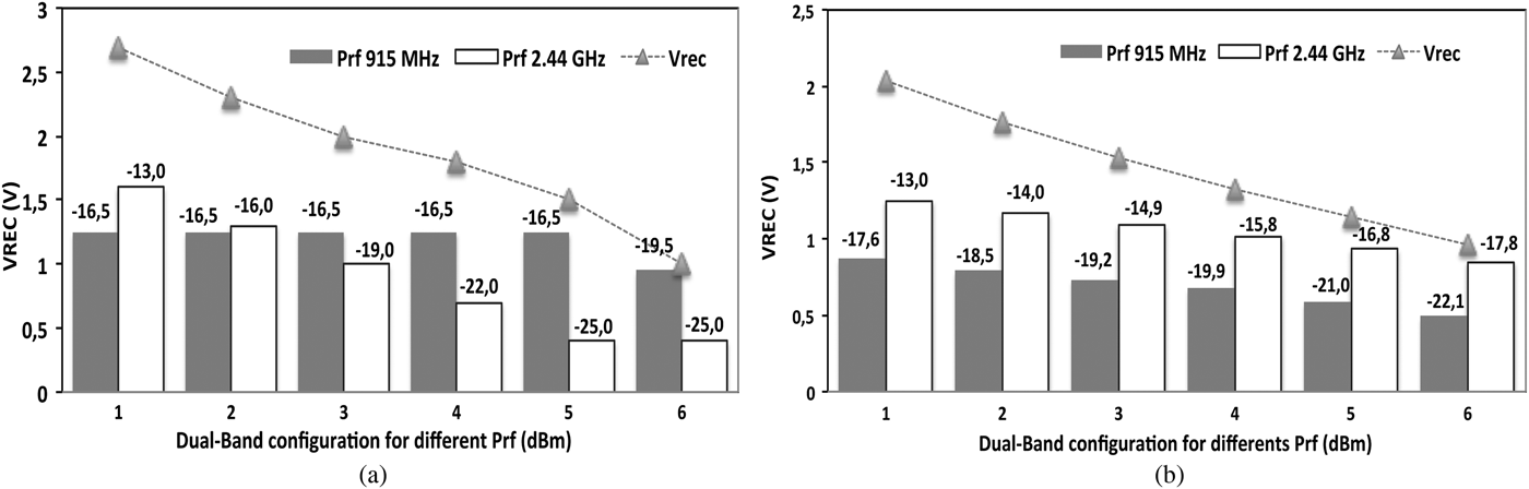
The power sensitivity is measured with the same scenario of Fig. 11 but the clock is disconnected. The output voltage is reported for different combination of collectable power at the antenna in a dual-band configuration.
To rectify a 1 V DC voltage, the patch-based harvester, Fig. 13(a), requires a two dual-band configuration: −19.5 dBm at 915 MHz and −25 dBm at 2.44 GHz, which is equivalent to an input power of −18.4 dBm (or 14 µW). For the same purpose the dipole-based harvester, Fig. 13(b), needs a dual-tone of −22.1 dBm at 915 MHz and −17.8 dBm at 2.44 GHz. The equivalent input power of this two-tone signal is −16.5 dBm (or 22 µW). The patch-based harvester exhibits a better sensitivity than the dipole harvester for the same reason exposed in the part A of this section. In Fig. 6, which reports the power sensitivity of the rectifier part only, the overall sensitivity is almost the same for the dipole harvester. It is improved by 1.8 dB for the patch harvester due to the additional gain of the antenna at 915 MHz.
Rectified voltage of the RF harvester based on patch (a) and arm dipole (b) antenna.
C) Discussion and comparison with the state of the art
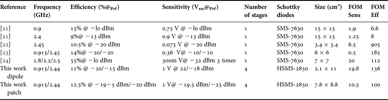
An important characteristic of a remote powered device is its size. Indeed it is expected to be as small as possible to make it unobtrusive to our closest environment. In a scenario of RF harvesting, the antenna footprint determines the compactness of a harvester operating ultra-high-frequency bands. To complete the comparison between the two harvesting modules developed in this work, two figures of merit, FOM sens and FOM eff, including the size of the antenna, are proposed in (2) and (3).
 $$FO{M_{sens}} = \displaystyle{{{V_{REC@Psens}}(V)} \over {{{({P_{sens}}({\rm \mu W})} / {100\,{\rm \mu W}}}) \times ({{{A_{ant}}({\rm c}{{\rm m}^2})} / {100\,{\rm c}{{\rm m}^2}}})}}$$
with P sens the input RF power required to provide V REC@Psens the unloaded rectified output DC voltage, and A ant the area of the antenna.
 $$FO{M_{eff}} = \displaystyle{{\eta (\% )} \over {({P_{eff}}({\rm \mu W})/100\,{\rm \mu W}) \times ({A_{ant}}({\rm c}{{\rm m}^2})/100\,{\rm c}{{\rm m}^2})}}$$
with P eff the input RF power required to achieve η the overall power efficiency.
FOM sens and FOM eff do not represent the same scenario of application. The FOM sens illustrates the capability of the rectenna to start collecting energy and store it in an element such as a capacitor or a battery to further release it. FOM eff demonstrates the capability of the RF harvester to yield “on time powering”: the rectenna is connected to an application and supply it on time. Both are reported in Table 1, which also includes some references of the state of the art. The ability of the proposed rectenna to simultaneously operate in two frequency bands, significantly improves the power sensitivity.
Comparison with the state of the art.
According to Table 1, the patch-based harvester exhibits the highest sensitivity to rectify 1 V with a dual-tone featuring: −19.5 dBm at 915 MHz and only −25 dBm at 2440 MHz. The FOM sens represents the trade-off between the sensitivity performances of a rectenna and the antenna area. The FOM eff rates the efficiency performances to the antenna area. For these two figures of merit, the rectenna based on the multi-arm dipole element yields the best trade-off, both for FOM sens and FOM eff, compared with the patch-based solution. This dual tone and multi-arm dipole harvester is close to the work proposed in [Reference Song, Huang, Zhou, Zhang, Yuan and Carter24] which exhibits the highest FOM sens reported so far in the literature to our knowledge.
V. CONCLUSION
The range of power collectable in a scenario of RF harvesting varies from −15 to −25 dBm. To address this purpose the rectenna proposed in this work are optimized to operate at an RF input power close to −20 dBm (or 10 µW). To further improve the ability to collect the RF energy, these rectenna, developed with Schottky diodes HSMS285 from Avago, perform a concurrent harvesting in the 915 MHz and 2.44 GHz ISM bands. The harvester including a patch antenna implemented on a 1.6 mm FR4 PCB achieves the highest sensitivity. It provides a 1 V-rectified voltage for a dual-tone excitation of −19.5 dBm at 915 MHz and −25 dBm at 2.44 GHz. For these conditions of operation the rectenna yields a power efficiency of 12.5%. To take into account the dimensions of the harvester, two figures of merit, FOM sens and FOM eff including the size of the antenna, respectively, related to the power sensitivity and the power efficiency are proposed. The rectenna developed with the arm dipole element exhibits the highest figures of merit. A case of application is proposed with the remote powering of a digital clock consuming 1 V/5 µA. The patch-based harvester turns on the device with a dual-tone excitation at the antenna of −19.5 dBm at 915 MHz and −20 dBm at 2.44 GHz. For the same scenario the harvester connected to the multi-arm dipole element needs a power of −22.1 dBm at 915 MHz and −17.8 dBm at 2.44 GHz.
ACKNOWLEDGEMENTS
The authors would like to thank the Engineering Department of the University of Bordeaux for funding support and IMS Lab for facilities.
Ludivine Fadel received the Ph.D. degree in Electrical Engineering from the University of Bordeaux, France, in 2004. She is an Associate Professor at Bordeaux University and her main research interests include wireless power transfer and energy harvesting, materials and printing technologies for RF application.
Laurent Oyhenart received the Ph.D. degree in Electrical Engineering from the University of Bordeaux, Bordeaux, France, in 2005. Currently he is an Associate Professor with the University of Bordeaux and develops his research activities in the IMS laboratory. His research interests include computational electromagnetics, photonic crystals, and antenna synthesis.
Romain Bergès is a Ph.D. student at IMS Laboratory. He received his Master from Bordeaux University in Electronic, in 2014. His current research focuses on RF Energy Harvesting.
Valérie Vigneras is a full professor in the Polytechnic Institute of Bordeaux and conducts research in the IMS Laboratory on complex structures (mixtures, structured media, and self-assembled media) both by simulation to predict or optimize their properties and by characterization before their integration in high-frequency systems (antennas, electromagnetic compatibility, and radar shieldness).
Thierry Taris is a full professor at the Bordeaux Institute of Technolgy (Bx-INP). He joined the IMS Laboratory in 2005 where his research interests are related to the radio-frequency integrated circuits in Silicon technologies.