I. INTRODUCTION
Vanadium oxide (VO2) exhibits a sharp first-order semiconductor-to-metal transition (SMT) at 68 °C, where the crystal structure changes from monoclinic to tetragonal (metal) at high temperatures. In VO2 single crystal, the typical SMT characteristics involve more than four orders of magnitude change in resistivity and a drastic drop in far infrared (IR) transmittance.Reference Morin1, Reference Nag and Haglund2 Since the phase transformation involves crystal distortions, it is envisaged that repeated thermal cycles across the transition temperature can lead to cracking of bulk VO2 crystals making them unsuitable for practical device applications. On the other hand, thin films are able to withstand these distortions; therefore, practical devices needing repeated thermal cycling can be fabricated using only thin films. However, fabrication of high-quality VO2 thin films with desirable properties requires a good control over epitaxial growth procedure, as the SMT characteristics of VO2 thin films are known to be a strong function of epitaxial characteristics, defects, microstructure, and stoichiometry.Reference Narayan and Bhosle3, Reference Griffiths and Eastwood4 Recently, high-quality VO2 thin films have been grown on c-sapphire, r-sapphire, and Si (100) substrates with yttria-stabilized zirconia (YSZ) buffer layers using the paradigm of domain epitaxy.Reference Yang, Aggarwal, Gupta, Zhou, Narayan and Narayan5, Reference Gupta, Aggarwal, Gupta, Dutta, Narayan and Narayan6 SMT properties of these films were also found to depend upon their defect content, and the properties were rationalized according to the phenomenological model presented by Narayan and Bhosle.Reference Narayan and Bhosle3 Detailed understanding of the role of defects in the modification of SMT characteristics of VO2 thin films is also important from the technological point of view since SMT properties can be tuned according to the device applications. Previous attempts to modify the SMT characteristics of VO2 thin films include proton irradiation, low-energy (few hundreds of eV) ion bombardment, and electron beam (MeV) irradiation.Reference Case7–Reference Lin, Lu, Liu, Lu and Feng10 In all of these cases, damage due to the displacement cascades is the dominant mechanism through which defects are generated in the films.Reference Nastasi, Mayer and Hirvonen11 Furthermore, the nuclear stopping is not constant throughout the film thickness for these low-energy implants and, therefore, the effects are not uniform, which renders considerable ambiguity with respect to distribution of defects and their role in producing changes in properties of VO2.
In this article, we have investigated the effect of swift heavy ion (SHI) irradiation on the SMT of epitaxial VO2 thin films. The unique advantage of SHI irradiation of materials is the production of nanometer-sized cylindrical zones, so-called ion tracks, provided the electronic energy loss crosses the threshold value. The number density of these ion tracks can be controlled by ion beam parameters such as fluence. Microstructure and defect content can be controlled by ion-irradiation parameters, such as ion type and energy, which dictate the dominant energy transfer mechanism. Under SHI irradiation, the energy loss through electronic stopping dominates and the energy is deposited uniformly into the entire thickness of the film. This energy is transferred mostly into electronic excitations, which, in turn, gets transferred to the lattice via electron–phonon coupling. This can cause extremely rapid (on the order of few picoseconds) heating and quenching in the localized regions along the ion path leading to the formation of a latent ion track. In our experiments, we have carefully chosen the energy of the ions such that electronic stopping power remains essentially constant throughout the thickness of the film.
II. EXPERIMENTS
VO2 thin films were grown epitaxially on Si (100) with cubic YSZ as an intermediate layer using pulsed laser ablation technique. The Si (100) substrates were cleaned ultrasonically in acetone and methanol. YSZ buffer layer (∼40 nm) was deposited at 650 °C for, first, 400 pulses in vacuum and then, 600 pulses in 5.4 × 10⁻⁴ Torr of oxygen pressure. Subsequently, VO2 thin films were deposited for 4500 pulses (∼225 nm) at 500 °C in 10–12 mTorr oxygen pressure. KrF excimer laser of wavelength 248 nm with pulse duration of 25 ns was used. For deposition of all layers, pulse energy density at the target was 2–3 J/cm2 and pulse rate was kept at 5 Hz. After the deposition, all samples were cooled to room temperature at a rate of ∼20 °C/min. Samples were irradiated using SHIs (200 MeV Au ions) at different fluences ranging from 1 × 10¹⁰ to 1 × 10¹³ ions/cm2. The SHI irradiation influences the structural and electrical properties of VO2 thin films by the introduction of defects in a controlled fashion with varying ion fluences. In this article, we present the effects of SHI irradiation on structural and electrical (SMT) characteristics of the VO2 thin films. The changes in SMT characteristics are shown to correlate strongly with the changes in crystalline as well as electronic structure of the VO2 thin films. The VO2/YSZ/Si(001) epitaxial heterostructures were grown using KrF pulsed excimer laser (pulse duration 25 ns) with fluence of 2–3 J/cm2 and repetition rate of 5 Hz. A complete description of deposition procedure can be found elsewhere.Reference Gupta, Aggarwal, Gupta, Dutta, Narayan and Narayan6 The SHI irradiation on these films was performed at Inter University Accelerator Center, New Delhi, India, in Materials Science beam line. The crystalline structure of the thin film heterostructure was determined using an X’Pert PRO MRD HR x-ray diffraction (XRD) system with CuKα radiation. Micro-Raman data of pristine and irradiated films were recorded with a Horiba Jobin Yvon LabRam ARAMIS using a 633-nm laser excitation at room temperature. To determine the oxidation states in the as-deposited and the irradiated VO2 films, x-ray photoelectron spectroscopy (XPS) analysis of the films was carried out in a Kratos Axis Ultra x-ray photoelectron spectrometer using Al Kα x-ray source. The values corresponding to the C 1s peak were used as a reference for the spectrum analysis. A Keithley 2400 sourcemeter was used to characterize SMT by measuring the resistance of VO2 films as a function of temperature.
III. RESULTS AND DISCUSSION
Nuclear and electronic stopping powers (S n and S e, respectively) of SHI in VO2 matrix were calculated using stopping and range of ions in matter (SRIM) simulations.Reference Ziegler, Biersack and Littmark12 For ion energies used in this study, the values of S e in VO2 were about 2009 eV/Å while S n was only ∼16 eV/Å. Nuclear stopping mechanism dominates at lower ion energies (<1 MeV), whereas the electronic stopping is the dominant energy loss mechanism at higher energies. In nuclear stopping, ions collide with the target atoms elastically and lose their energy to the target lattice causing atomic displacements, which lead to the creation of Frenkel defects (vacancy and interstitial pairs). However, electronic stopping is inelastic in nature and dense electronic excitations are induced at high ion energies. The energy stored in electronic excitations is transferred rapidly to the phonons as the electron–phonon relaxation times are less than a picosecond. These dense electronic excitations can raise the temperature to several thousands of degrees, according to thermal spike model, within a narrow cylindrical zone of a few nanometers around the ion path for short time durations.Reference Toulemonde, Constantini, Dufour, Meftah, Paumier and Studer13 The electronic excitations are also known to cause breaking of chemical bonds via Coulomb explosion, and this can lead to significant disorder in the VO2 matrix around the ion tracks.Reference Avasthi, Assmann, Notle, Mieskes, Ghosh and Mishra14 Using SRIM/transport of ions in matter calculations, it was simulated that the projected range of ions, of energies used in this study, was of the order 18 μm, which was much larger than the thickness of VO2 films (∼220 nm), and the electronic energy loss (S e) is almost constant throughout the film thickness.Reference Ziegler, Biersack and Littmark12 Therefore, the effects of electronic excitations on the structural and electronic properties of VO2 thin films are expected to be uniform across the entire thickness of the films.
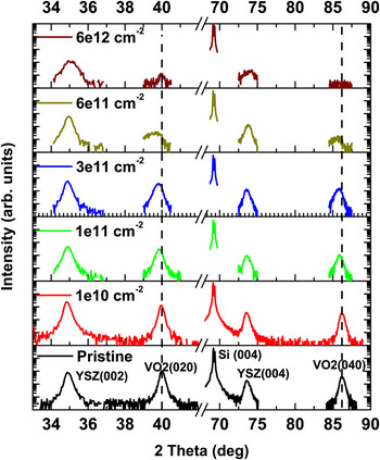
Figure 1 shows the comparison of XRD θ–2θ patterns of a typical Si/YSZ/VO2 heterostructure samples in pristine and ion-irradiated conditions with different fluences of 200 MeV Au ions. Detailed characterization, using XRD, of the epitaxial orientation of as-deposited VO2 thin films has been reported elsewhere.Reference Gupta, Aggarwal, Gupta, Dutta, Narayan and Narayan6 It can be clearly seen that as the ion fluences are increased gradually, peak intensity for VO2 peak decreases and full width at half maximum (FWHM) increases. It was also confirmed by full range 2θ scan that no other vanadium oxide phases were present. Lower intensity and higher FWHM of the VO2 (020) peaks suggest that the ion irradiation causes disordered regions in the films, which increase with ion fluence. Also, the VO2 peak for ion-irradiated films was found to shift to a lower 2θ compared to the as-deposited films. As discussed in our earlier work, as-deposited films are under compressive strain in the out-of-plane direction.Reference Gupta, Aggarwal, Gupta, Dutta, Narayan and Narayan6 Relaxation of this compressive strain is likely to occur upon SHI irradiation as SHI irradiation caused creation of defects and disordered regions, which can lead to a shift in the VO2 peak position. It was also seen that above the fluence of 6 × 10¹¹ ions/cm2, VO2 (020) peak disappears almost completely, which is due to the fact that overlapping of ion tracks (defective disordered regions) occurs above this fluence. Single-ion impact leads to a cylindrical (∼7 nm radius) disordered zone throughout the film thickness, and after the overlapping fluence (which is ∼1 × 10¹² ions/cm2), whole volume of the film is full of disordered zones. At this fluence, no pristine VO2 regions remain and the entire VO2 film becomes highly disordered or amorphous causing the near disappearance of the VO2 peak. It can also be seen from Fig. 1 that FWHM of YSZ (002) reflections also increases with increasing fluence, which confirms that ions pass through the entire thickness of VO2 films.
Comparison of x-ray diffraction patterns of a pristine Si(100)/YSZ/VO2 heterostructure and swift heavy ion (SHI)-irradiated VO2 films with 200 MeV Au ions at varying ion fluences.

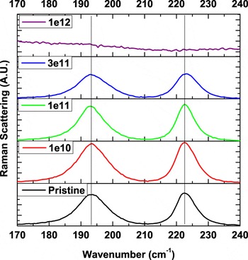
Creation of defects and disordered regions upon SHI irradiation is also evident from Raman spectra of pristine and irradiated VO2 films. Figure 2 shows, for comparison, the Raman spectra of as-deposited and irradiated VO2 films at different fluences. The spectra were calibrated using Si peak at 520.07 cm−1 as a reference. Raman spectrum of the as-deposited film shows distinct peaks at 193 and 223 cm−1, corresponding to Ag Raman mode.Reference Schilbe15 As the VO2 films are irradiated with increasing ion fluence, these peaks shift to lower frequency and FWHM increases. It is envisaged that this shift occurred due to creation of defects (presumably oxygen vacancies) in disordered ion-track regions, and FWHM increased consequently due to increasing disorder (loss of symmetry) in the films. Similar phenomenon of Raman peak shifts has been observed in PbTiO3, where increasing amount of shift to lower frequency was attributed to increasing oxygen vacancy concentration.Reference Nishida, Osada, Takeuchi, Yosiaki, Sakai, Ito, Ikariyama, Kamo, Fujisawa, Funakubo, Katoda and Yamamoto16 The idea that Raman peaks shift to lower frequency with the introduction of oxygen vacancies is also supported by the observations that Parker made in which shifts to higher frequencies for oxygen-rich VO2 were observed.Reference Parker17 Similar to XRD results, in the case of Raman spectroscopy also, it was observed that the distinct Raman peaks disappear at 1 × 10¹² ions/cm2 fluence. This confirms that the ion fluence of 1 × 1012 cm−2 is above the threshold of overlapping fluence where ion tracks overlap with each other. Therefore, for the ion-irradiated films, Raman peaks corresponding to VO2 vibrational modes disappear due to a high degree of disorder in overlapping ion tracks through the whole thickness of the VO2 film.
Raman spectra of the pristine and ion-irradiated VO2 films (with 200 MeV Au ions), shown one below the other for comparison. Silicon peak at 520.07 cm-1 was used to calibrate the spectra.

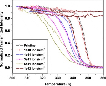
The IR transmission measurements, using an IR laser (wavelength = 1.5 μm), were also performed to further elucidate the effect of SHI on epitaxial VO2 thin films. These results are presented in Fig. 3, where % transmittance has been plotted as a function of temperature with varying ion doses. It can be clearly seen that optical switching behavior of irradiated VO2 thin films became increasingly diffused (broad) with increasing ion fluence. At overlapping fluence of 1 × 10¹² ions/cm−2, no significant change in IR transmittance was observed. Although normalized transmittance has been plotted in Fig. 3, it was observed that with increasing ion dose, transmittance of the sample under test decreased and detector’s gain had to be increased to get good signal-to-noise ratio. It is clear from Fig. 3 that controlled tailoring in SMT of VO2 can be obtained by carefully controlling the ion fluence.
Comparison of infrared transmission of as-deposited and SHI-irradiated (with 200 MeV Au ions) VO2 thin films as a function of temperature with varying ion fluences.

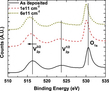
Figure 4 shows, for comparison, XPS spectra of as-deposited and ion-irradiated VO2 films. As shown in the figure, V2p3/2 peak for ion-irradiated films shifts to lower binding energy values as the ion fluence increases, signifying the increasing concentration of V3+ oxidation state of vanadium with increasing ion fluence.Reference Moshfegh and Ignatiev18, Reference Sawatzky and Post19 In the disordered regions which are created due to SHI irradiation, loss of oxygen is likely to occur which leads to a shift of spectrum toward higher binding energies. It is also envisaged that localized heating around the tracks leads to oxygen deficiencies in the films and increasing concentration of V3+ with respect to the as-deposited sample.
Comparison between x-ray photoemission spectra of as-deposited and ion-irradiated VO2 (with 200 MeV Au ions) thin films.

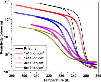
A comparison of resistivity, as a function of temperature, of as-deposited and ion-irradiated films is shown in Fig. 5. It can be clearly seen that the as-deposited VO2 films show a first-order SMT, and the resistance drops sharply by ∼3 orders of magnitude. However, ion-irradiated films start to exhibit an increasingly broad transition with increasing ion fluence. It is expected that as the number of defective sites (disordered regions/ion tracks) in the films are increased with increasing ion fluence, the amplitude of the transition will be smaller due to higher defect content. Also, as the ion fluence is increased, hysteresis width of the transition decreases as there will be increasingly more nucleation sites available for the transition to occur. It should also be noted that resistivity of the films decreases in the low-temperature (semiconducting) region as number of carriers (electrons in the case of VO2) increases with increasing concentration of V3+ arising from increasing ion fluence. Also, in the high-temperature (metallic) regions, resistivity increases with increasing ion fluence as the carrier scattering is expected to be proportional to the defect content in the VO2 thin films. For the 6 × 10¹¹ ion/cm2 fluence, transition becomes similar to that of near-amorphous films.Reference Klimov, Timofeeva, Khanin, Shadrin, Il’inskiÏ and Silva-Andrade20 This phase transition is of second-order type and less of structural nature where pairing of V atoms, unit cell doubling, and charge ordering is critical. This is similar to the Mott type, a diffused second-order transition, which would typically be expected from disordered/amorphous VO2 thin films.
Comparison between resistivity of as-deposited and ion-irradiated thin films (200 MeV Au ions) plotted against temperature (T).

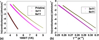
For the as-deposited films, plot of ln(conductivity) against 1/T in semiconducting phase yields an Arrhenius-type of straight line [shown in Fig. 6(a)] with activation energy ∼0.19 eV. This value is comparable to what has been reported in the literature, confirming high quality of as-deposited films.Reference Ko and Ramanathan21 An interesting point concerns the increasing deviation of ion-irradiated VO2 films from Arrhenius behavior in the semiconducting region. For ion-irradiated films, ln(conductance) against T −1/4 plot fits a straight line that suggests a “quasiamorphous” description of the resistivity of VO2 [shown in Fig. 6(b) for 3 × 10¹¹ and 6 × 10¹¹ ion/cm2 fluence].Reference Von Schulthess and Wachter22 This can be explained by taking into account the defects created upon SHI irradiation. In the present case of ion-irradiated films, SHI irradiation can induce large number of localized states, present in the bandgap, by introduction of disorder in the VO2 thin films and also the presence of V3+ ions (as seen in XPS spectra) can lead to mid-gap defect states. This leads to a variable-range hopping transport behavior in the ion-irradiated films, where ln(conductance) follows a linear relationship with T −1/4. This is in agreement with previous reports, where similar deviations from Arrhenius behavior have been observed in VO2 films upon proton irradiation where radiation-induced defect states were believed to be responsible.Reference Leone, Trione and Junga9
(a) Plot of ln(conductance) against 1/T for as-deposited film and ion-irradiated films and (b) plot of ln(conductance) against T −1/4 for ion-irradiated films at 3 × 10¹¹ and 6 × 10¹¹ ion/cm2 fluence.

IV. CONCLUSIONS
In conclusion, we have shown that controlled modifications in SMT in VO2 thin films were induced by the introduction of defects upon SHI irradiation. The ion irradiation creates disordered regions containing defects around ion tracks in epitaxial VO2 thin films. Dense electronic excitations caused by electronic stopping, the dominant energy loss mechanism at these energies, facilitate the introduction of defects in VO2 matrix. Our electrical resistivity measurements and XRD combined with XPS studies support the observation of defect-induced Mott (electronic) type of SMT in VO2 thin films. It is envisaged that the ion irradiation, where nature/extent of ion–VO2 interactions and resulting defect content can be controlled by changing the ion-irradiation parameters, provides an interesting opportunity to understand the role of defects in SMT and to design a new class of VO2-based smart sensor devices. Further studies are being conducted to understand, in detail, the nature of these defects and their influence on magnetic properties.
ACKNOWLEDGMENTS
The authors express our gratitude to Prof. Rene Lopez of the University of North Carolina at Chapel Hill for letting A.G. use his setup for infrared transmission measurements. We acknowledge the financial support from the National Science Foundation under award No. 0803663 (Division of Materials Research).