Introduction
The high-pressure high-temperature (HPHT) technique that mimics the natural formation process of diamond deep inside the earth and chemical vapor deposition (CVD) that works far from thermodynamic equilibrium below ambient pressure are synthesis routes that were discovered nearly contemporaneously in the first half of the 1950s. While the former quickly reached the level of an industrial production method, CVD of diamond was not considered a serious alternative until technologically relevant growth rates in the micron-per-hour range were shown by Japanese scientists in the 1980s (see the Introductory article in this issue and Reference 1). A large number of different methods for the activation of the gas phase in the CVD process were subsequently developed. They facilitated an easy overcoming of the inherent size limitations of the HPHT technique (∼1 cm) and provided a variety of polycrystalline diamond layers differing in grain size, texture, impurity content, resistivity, and transparency.
Polycrystalline diamond has been established in various demanding applications (heat spreaders, infrared and microwave windows, and wear resistant coatings). In several applications, however, the polycrystalline nature prevents diamond devices from achieving the ultimate performance levels expected from single crystal diamond (SCD) parameters. As a consequence, electronic devices suffer from drastically reduced charge carrier mobilityReference Nebel, Nebel and Ristein2 and detectors from incomplete charge collection.Reference Isberg, Hammersberg, Twitchen and Whitehead3
The fundamental feasibility of high-quality SCD synthesized by CVD has already been demonstrated convincingly. In homoepitaxial samples of diamond grown on HPHT crystals, mobility values of holes and electrons are close to the theoretical limit,Reference Isberg, Hammersberg, Johansson, Wikström, Twitchen, Whitehead, Coe and Scarsbrook4,Reference Nesladek, Bogdan, Deferme, Tranchant and Bergonzo5 and a charge collection efficiency approaching unity can be achieved.Reference Berdermann, Pomorski, de Boer, Ciobanu, Dunst, Grah, Kiš, Koenig, Lange, Lohmann, Lovrincic, Moritz, Morse, Mueller, Pucci, Schreck, Rahman and Traeger6 In order to profit from these outstanding results, technology for the reproducible manufacturing of SCD with appropriate size and structural quality is required. This article describes the different approaches that are currently being undertaken to reach this goal.
In the first part of this article, the issue of high rate homoepitaxial growth is addressed. Basically, several different activation methods have the potential for deposition rates of several 10 µm/h.Reference Bachmann and Davies7 Here, we focus on microwave plasma-assisted chemical vapor deposition (MPACVD) as the most prominent method that combines excellent film purity with high growth rates that are homogeneous over acceptable areas. Furthermore, tiling as a powerful concept to increase the lateral size is described. Heteroepitaxy provides a completely different approach to synthesize SCD on scalable substrates. In the second part of the article, after a brief survey of explored substrate materials, we concentrate on iridium, describing the characteristics of the nucleation process on this unique template material, and the specific defect structures inherent to heteroepitaxial diamond. Finally, present and potential future applications are discussed.
Homoepitaxial deposition of SCD by MPACVD
The first report of homoepitaxial SCD synthesis was by Kamo et al.Reference Kamo, Yurimoto and Sato8 in 1988. Typical for the early MPACVD experiments was a low microwave power density plasma (<5 W/cm3) operating in the 20–100 Torr pressure regime. To guarantee an acceptable crystal quality, CH4 concentrations <1% were chosen, which resulted in growth rates ≤1 µm/h. Attempts toward an increase in growth rate by simply adding more CH4 (e.g., 5%) led to the formation of defects (e.g., by deposition of sp Reference Nebel, Nebel and Ristein2 carbon) by secondary nucleation and by twinning. Teraji reviewed these early studies in 2006.Reference Teraji9
Increasing deposition rates while maintaining a high crystalline quality was a basic challenge in the subsequent years. Since CVD growth on {100} crystal faces yields the lowest density in structural defects, nearly all experimental work in homoepitaxy was concentrated on (001)-oriented substrates. The initial communications that revealed the feasibility of SCD with rates of 50–150 µm/h by MPACVD were reported in the mid-1990s and early 2000s.Reference McCauley and Vohra10,Reference Yan, Vohra, Mao and Hemley11 The key to this progress was the successful operation at high microwave discharge power density and high gas pressure (100–400 Torr) combined with the development of corresponding reactor technologies.Reference Williams and Jackman12–Reference Liang, Yan, Meng, Lai, Krasnicki, Mao and Hemley29 The introduction of 915 MHz microwave reactors with their higher wavelength as compared to the common 2.45 GHz systems facilitated a corresponding increase in the maximum size of the plasma discharge. This development marked an important step toward upscaling the high pressure processes to larger areas. The processes that take place in this new process regime have been explored in detail.Reference Sternschulte, Bauer, Schreck and Stritzker15,Reference Yamada, Chayahara, Mokuno, Soda, Horino and Fujimori19,Reference Silva, Achard, Brinza, Bonnin, Hassouni, Anthonis, De Corte and Barjon30,Reference Harris and Goodwin31
The common features of diamond growth by MPACVD include (1) a microwave discharge that heats the H2/CH4 feed gas mixtures to 2500–4000 K, thereby producing the appropriate growth radicals (i.e., H and CH3 ),Reference Harris and Goodwin31 (2) the presence of these growth species in the boundary layer above the substrate, and (3) a growth surface that is cooled to 850–1450 K. Additional gas species such as oxygen or nitrogen in the gas mixture are frequently used. Traces of N2 (typically several 10 ppm) can dramatically increase the growth rate.Reference Müller-Sebert, Wörner, Fuchs, Wild and Koidl32 However, since it deteriorates the diamond quality (e.g., causing a reduced mobility-lifetime product),Reference Secroun, Brinza, Tardieu, Achard, Silva, Bonnin, De Corte, Anthonis, Newton, Ristein, Geithner and Gicquel33 nitrogen should be avoided during growth for electronic applications. Recently, it was reported that the power density required to sustain a microwave plasma can be reduced by the addition of chemically inert argon, an effect that is attributed to its lower heat conductivity.Reference Tallaire, Rond, Bénédic, Brinza, Achard, Silva and Gicquel34
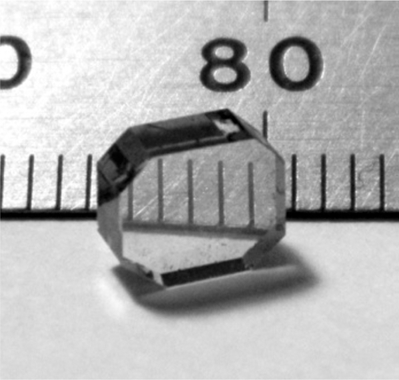
Increasing the process gas pressure from 50 to 300–400 Torr is accompanied by several fundamental changes. First, the size of the discharge (the “plasma ball”) shrinks, and the absorbed power density increases from 5–10 W/cm3 to 1000 W/cmReference Isberg, Hammersberg, Twitchen and Whitehead3.Reference Gu, Lu, Grotjohn, Schuelke and Asmussen26 Associated with this, the gas temperature and the density of radicals rises (e.g., for H and CH3 by factors of 1000 and 10, respectively).Reference Silva, Achard, Brinza, Bonnin, Hassouni, Anthonis, De Corte and Barjon30 The stronger activation of the gas phase expands the range of useful CH4/H2 compositions to 5–10%Reference Silva, Achard, Brinza, Bonnin, Hassouni, Anthonis, De Corte and Barjon30 and facilitates growth at temperatures well above 1000°C, where the fraction of free sites (dangling bonds) (i.e., potential adsorption sites for new growth species) is higher.Reference Butler, Woodin, Lettington and Steeds35 The contribution of all these processes facilitates an increase in the growth rate with process gas pressure well above the pure effect of the higher gas kinetic arrival rate at the diamond surface. Figure 1 shows an example of a SCD with physical properties comparable to natural Type IIa crystals (1–2% of all natural diamonds with almost no impurities, especially no measurable nitrogen substitution) that has been grown at high power density and pressure.
A colorless, Type IIa 1.25 carat diamond synthesized by microwave plasma-assisted chemical vapor deposition on a 7 × 7 mm2 high-pressure high-temperature seed crystal. The sample was laser cut and mechanically polished after growth. Reprinted with permission from Reference 38. © 2014 Elsevier.

Crystals with a size beyond 10 caratsReference Liang, Yan, Meng, Lai, Krasnicki, Mao and Hemley29 or with ultimate electronic properties have also been synthesized.Reference Isberg, Hammersberg, Johansson, Wikström, Twitchen, Whitehead, Coe and Scarsbrook4 In addition, high rate deposition over large areas and on multiple substrates has been demonstrated (see Figure 2).Reference Asmussen, Grotjohn, Schuelke, Becker, Yaran, King, Wicklein and Reinhard36
Microwave plasma-assisted chemical vapor deposition of single crystal diamond over 70 large 3.5 × 3.5 mm2 high-pressure high-temperature seed crystals.Reference Asmussen, Grotjohn, Schuelke, Becker, Yaran, King, Wicklein and Reinhard36 Growth conditions: 915 MHz excitation, MW power 11.5 kW, pressure 125 Torr, and 5–8% CH4/H2. The discharge diameter was >100 mm, and the substrate temperature varied between 1125°C and 1200°C across the substrate area. Reprinted with permission from Reference 36. © 2008 AIP Publishing.
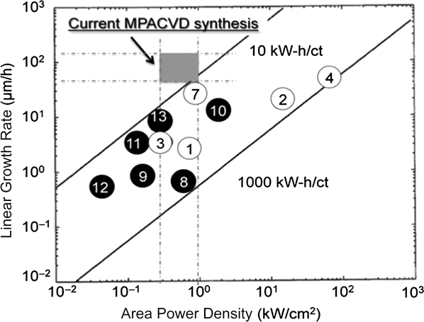
Electrical energy consumption for the activation of the plasma represents a major cost factor in SCD production. Figure 3 compares the values of power density and growth rate for different plasma reactor technologies.Reference Kuo37 The circles correspond to pre-1997 reactor technologies, while the shaded rectangular area indicates the current performance of MPACVD. Based on an energy price of 10 ct/kWh, the electrical energy cost per carat can be estimated to be ∼1 $/ct (with 1 ct = 0.2 g).
Linear growth rate and electrical-energy-efficiency/carat versus area power density for different diamond synthesis reactors.Reference Kuo37 (1) Hot filament chemical vapor deposition (CVD); (2) conventional DC; (3) enclosed DC arcjet; (4) atmospheric pressure DC arcjet; (7) RF thermal plasma; (8) magneto-microwave; (9) tubular microwave; (10) microwave plasma jet; (11) ASTeX bell jar microwave; (12) bell jar microwave (Michigan State University); and (13) high-pressure bell jar microwave (Michigan State University). The gray area indicates the region where current, state-of-the-art, high-pressure microwave plasma-assisted CVD (MPACVD) synthesis is located.
Single crystal seed recovery by laser cutting
Currently, the most commonly used seeds for homoepitaxial growth are commercially available Type Ib HPHT crystals that typically contain about 100 ppm of substitutional nitrogen. Their size ranges from 3.5 × 3.5 mm2 to 7 × 7 mm2. In order to limit production costs, reuse of seeds is imperative.
There are two principal methods of seed recovery: (1) slicing by laser cutting or (2) creation of a damaged layer using ion implantation (see following section on “cloning”). Seed recovery by laser cutting comprises the (1) separation of seed and grown material, (2) mechanical polishing of the seed’s top surface, and (3) edge trimming. As shown in Reference Reference Muehle, Becker, Schuelke and Asmussen38, the cyclic treatments (recycling of the seed crystals) do not cause measurable changes in the quality of the seed material. After ∼20 cycles, the seeds become too thin (∼250 µm) for the polishing step.
The structural quality of a SCD can surpass that of the Type Ib seed. Thus, in an alternative approach, the CVD grown crystals can be further used as seed crystals for homoepitaxy applying the same recovery procedures.Reference Lu, Gu, Grotjohn, Schuelke and Asmussen27
Cloning of diamond single crystals
A second concept that uses high-quality single crystals (typically also HPHT samples) as reusable templates for the homoepitaxial growth of SCD is often summarized under the expression “cloning of diamond substrates.”Reference Mokuno, Chayahara, Yamada and Tsubouchi39,Reference Yamada, Chayahara, Umezawa, Tsubouchi, Mokuno and Shikata40 It is comprised of (1) the creation of a thin, damaged layer buried several microns below the surface by high energy ion implantation,Reference Parikh, Hunn, McGucken, Swanson, White, Rudder, Malta, Posthill and Markunas41 (2) homoepitaxial CVD diamond growth on the implanted side of the crystal, and (3) lift-off by removal of the damaged layer.
Throughout the process, the loss in material is only ∼1 µm, and the mother crystal can be re-used to generate second and third copies, etc. Common to all these clones is an identical defect structure (e.g., threading dislocations), crystallographic off-angle and off-direction (i.e., the “DNA of a crystal”).
Homoepitaxial overgrowth of tiled substrates
Simple cloning can yield copies of identical size. However, technology calls for wafer size dimensions. A first attempt concentrated on a gradual increase in the top facet area during homoepitaxial growth by carefully tuning the growth parameters.Reference Silva, Achard, Brinza, Bonnin, Hassouni, Anthonis, De Corte and Barjon30 A second concept used side-surface growth, a method in which the lateral dimensions were increased by successively using the side faces as growth surfaces.Reference Mokuno, Chayahara, Yamada and Tsubouchi39 The third approach that facilitated the fastest increase in area was by mosaic growth.Reference Janssen and Giling42 This has recently been refined by using clones that had been produced as described before. They were arranged with high angular precision side by side, and finally the mosaic pattern was overgrown in a CVD process (see Figure 4). The identical off-axis orientation guarantees efficient bridging of the gap between the different crystals during the overgrowth.
Schema describing the different steps of the cloning and tiled growth concept. SCD, single crystal diamond. Reprinted with permission from Reference 40. © 2012 Elsevier.
After coalescence, the “copying” process can be applied to the complete monolithic diamond. In the meantime, plates with lateral dimensions of 20 × 20 mm2 and 20 × 40 mm2, which consist of four and eight clones, respectively, have been manufacturedReference Yamada, Chayahara, Mokuno, Umezawa, Shikata and Fujimori43,Reference Yamada, Chayahara, Mokuno, Tsubouchi and Shikata44 (see Figure 5).
A 40 × 20 mm2 homoepitaxial diamond sample produced by overgrowth of eight tiled clones. Reprinted with permission from Reference 44. © 2013 Elsevier.
Due to the high defect density, the connection lines cannot be used for semiconductor devices, but they may serve as “dicing lines” after fabrication of device structures in high-quality regions. Using this technique, 2-inch size diamond wafers are now available, and 3- or 4-inch wafers seem realistic in the near future.
Structural defects in homoepitaxial diamond
For the operation of diamond power semiconductor devices, crystal defects are a crucial issue. Extending the maximum output level of 1 A for current demonstration devicesReference Umezawa, Kato and Shikata45 toward 100 A operation will require a strong reduction in defect densities, especially of dislocations.
Threading dislocations in homoepitaxial SCD layers are preliminarily continuations of defects already existing in the seed crystal. In standard Type Ib crystals, their density is ∼105 cm–2. Analysis of the dislocations can be done by transmission electron microscopy (TEM), preferential etching,Reference Achard, Silva, Brinza, Bonnin, Mille, Issaoui, Kasu and Gicquel46 or synchrotron radiation x-ray topography.Reference Umezawa, Kato, Watanabe, Omer, Yamaguchi and Shikata47 These methods facilitate easy selection of very low-density HPHT seed crystals.Reference Sumiya, Toda and Satoh48
Additional dislocations can nucleate at the substrate surface (e.g., caused by the polishing treatment). Polishing damage has to be minimized, and remaining subsurface damage should be removed (e.g., by plasma etching before growth is started).Reference Friel, Clewes, Dhillon, Perkins, Twitschen and Scarsbrook49 A novel, very gentle polishing method assisted by UV light has recently been reported.50 It produces ultra-flat surfaces and thus suppresses the nucleation of new dislocations completely.
Heteroepitaxy on scalable substrates
Heteroepitaxy (i.e., the oriented growth of one crystalline material on the surface of another one) constitutes a promising alternative approach for synthesizing large-size single crystal diamond. It allows for the selection of substrate materials that are already available as standard large-size and high-crystalline-quality products. However, combining two different crystalline materials brings several new problems and challenges. For example, the substrate has to withstand the harsh diamond growth environment. The chemistry, crystal structure, and lattice parameters of the substrate and diamond have to match to an extent that facilitates a high perfection of the epitaxial alignment for the deposited layer.
Finally, heteroepitaxy on a foreign substrate involves a nucleation step. The high nucleation barrier resulting from diamond’s large surface energy represents a crucial challenge. Seeding with tiny diamond grains, a well-established technique for polycrystalline coatings on various substrates, was successfully modified to generate oriented diamond on different metal substrates (Pt(111),Reference Tachibana, Yokota, Kobashi and Shintani51 Ni(111) and Ni(001),Reference Zhu, Yang and Glass52 Co(111)53). However, this technique is difficult to control, and the crystalline quality of the obtained films was rather poor.
Currently, bias-enhanced nucleation (BEN)Reference Yugo, Kanai, Kimura and Muto54 is the most efficient process to generate epitaxial diamond islands. A negative DC voltage of typically 100–300 V is applied to the substrate. In the majority of cases, the procedure is executed during MPACVD. The microwave discharge is combined with a DC discharge that produces a localized region of higher electrical field strength in the plasma directly above the substrate, similar to the cathode fall region in a classical glow discharge.Reference Schreck, Baur and Stritzker55 As a consequence, positive ions are accelerated to energies that induce the critical processes for in situ nuclei formation at or shallowly below the surface.Reference Arnault and Girard56 Nucleation densities in the vicinity of 1011/cm2 can be obtained. By careful control of the BEN parameters, epitaxial nucleation of diamond has been achieved on various heterosubstrates such as Si,Reference Jiang, Klages, Zachai, Hartweg and Füsser57 3C-SiC,Reference Stoner and Glass58 and Ir.Reference Ohtsuka, Suzuki, Sawabe and Inuzuka59,Reference Schreck, Roll and Stritzker60 The next section focuses on Ir since it turned out to be unique in terms of the nucleation mechanisms involved and the attainable diamond crystal quality; refer to the literature for more details about heteroepitaxy on other substrates.Reference Schreck and Sussmann61–Reference Schreck, Hörmann, Roll, Bauer and Stritzker64
Oriented nucleation on iridium surfaces
BEN of diamond on Ir differs fundamentally from the corresponding process on all other surfaces. Immediately after BEN, no epitaxial diamond crystals are observable. Instead, scanning electron microscopy (SEM) images using the appropriate in-lens detector reveal pattern formation consisting of well-defined bright areas called “domains.”Reference Schreck, Bauer, Gsell, Hörmann, Bielefeldt and Stritzker65–Reference Chavanne, Barjon, Vilquin, Arabski and Arnault67 In subsequent standard growth experiments, diamond crystals only evolved from the domain areas,Reference Schreck, Bauer, Gsell, Hörmann, Bielefeldt and Stritzker65 with local area densities of 2–3 × 1011 cm–2.Reference Brescia, Schreck, Gsell, Fischer and Stritzker68 High-resolution TEM (HRTEM) and x-ray photoelectron spectroscopy (XPS) observations showed that the deposit formed by the BEN treatment consists of a closed carbon layer with thickness ranging from 1–2 nm68 to 8 nm.Reference Vaissière, Saada, Bouttemy, Etcheberry, Bergonzo and Arnault69 However, neither HRTEM nor other electron diffraction techniques could detect crystalline diamond structures in this layer. More recently, an SEM investigation demonstrated the localization of diamond nuclei before growth in the “domains” (see Figure 6).
Iridium surface observed after 30 min bias-enhanced nucleation (BEN) (left side) and after 5 min chemical vapor deposition (right side) by field emission gun SEM. Comparative image analysis underlines the correlation between nuclei locations (in blue) and diamond crystals (in green).Reference Vaissière, Saada, Bouttemy, Etcheberry, Bergonzo and Arnault69
The most meaningful proof for the presence of crystalline diamond structures in the pure nucleation layer was derived from x-ray photoelectron diffraction (XPD) measurements.Reference Kono, Shiraishi, Plusnin, Goto, Ikejima, Abukawa, Schimomura, Dai, Bernarski-Meinke and Golding70,Reference Gsell, Berner, Brugger, Schreck, Brescia, Fischer, Greber, Osterwalder and Stritzker71 The data suggest a highly defective nature of the diamond structure in the BEN layer, which can be attributed to the harsh ion bombardment during BEN. The bombardment suppresses vertical diamond growth completely,Reference Hörmann, Schreck and Stritzker72 but lateral growth seems to be possible, thus yielding a conclusive mechanism for the pattern formation (“domains”).Reference Schreck and Sussmann61
The lateral growth can also make plausible the observation that the diamond crystals that evolve from the nucleation layer after the BEN process are essentially all epitaxially oriented with a low angular spread. This excellent initial alignment of epitaxial crystals on iridium provides the basis for very efficient mechanisms causing strong further reduction in mosaic spread in the subsequent growth of thick layers.Reference Schreck, Schury, Hörmann, Roll and Stritzker73
Routes for upscaling of diamond on iridium
Bulk Ir single crystals are not a technologically relevant option due to prohibitive price and lack of availability. Instead, heteroepitaxial Ir films on MgO (001),Reference Saito, Tsuruga, Ohya, Kusakabe, Morooka, Maeda, Sawabe and Suzuki74 SrTiO3 (001),Reference Schreck, Roll and Stritzker60 Al2O3 (11–20),Reference Bednarski, Dai, Li and Golding75 or YSZ/Si (001)76,77 have been used for nucleation and growth studies of diamond on Ir. In principle, all these substrates can be used for upscaling the epitaxial crystal growth process: available wafer sizes are at least 2 inches for SrTiO3 and MgO, 8 inches for Al2O3, and 12 inches for Si. From production points of view, Si offers the important advantage of a better fit in the coefficient of thermal expansion with diamond, which results in much lower thermal stress after cool-down from growth temperature than oxide single crystals.Reference Gsell, Bauer, Goldfuß, Schreck and Stritzker76
Heteroepitaxial growth of Ir on Si requires the insertion of a buffer layer in order to avoid chemical interaction. SrTiO3 and yttria-stabilized zirconia (YSZ) turned out to be suitable candidates. In the meantime, Ir/YSZ/Si samples with (001) and (111) orientations are available in 4-inch wafer size, and epitaxial diamond films have been deposited on both of these types of substrates.Reference Fischer, Gsell, Schreck, Brescia and Stritzker77,Reference Fischer, Brescia, Gsell, Schreck, Brugger, Greber, Osterwalder and Stritzker78
Defects in heteroepitaxial diamond films
During growth, the structure of heteroepitaxial diamond layers passes through three different stages: (1) tiny oriented islands merge to form a mosaic crystal consisting of individual single crystal blocks (2). After ∼10–30 µm, the polygonized grain boundary network separating these blocks dissolves into single and clusters of dislocations (3). Prolonged growth in stage 3 up to a thickness d of ∼1 mm yields a continuous reduction in dislocation density.Reference Stehl, Fischer, Gsell, Berdermann, Rahman, Traeger, Klein and Schreck79 Mathematically, the average dislocation density follows a 1/d scaling law (see Figure 7). With values below 108 cm–2 after 1 mm growth, the dislocation density has passed through the range that is typical for standard natural Type IIa crystals (108–109 cm–2).Reference Balmer, Brandon, Clewes, Dhillon, Dodson, Friel, Inglis, Madgwick, Markham, Mollart, Perkins, Scarsbrook, Twitchen, Whitehead, Wilman and Woollard80 Provided that the 1/d behavior remains valid up to higher thicknesses, further defect reduction seems difficult by simple growth. Alternative concepts like epitaxial lateral overgrowth (ELO) may offer a new option for further improvement. Sawabe’s group has investigated a modification of the ELO concept.Reference Ando, Kamano, Suzuki and Sawabe81 They found that patterning of the BEN layer can drastically reduce the dislocation density at a very early stage of growth.
Red data points are dislocation density as deduced from the measurement of the number of etch pits formed in a CO2/H2 microwave plasma versus the crystal thickness. The blue data points were derived from plan view TEM images. Reprinted with permission from Reference 79. © 2013 AIP Publishing.
Current and potential future applications
In principle, CVD diamond grown by homoepitaxy can be applied in all areas in which natural or HPHT diamond is already employed in industry, for example as cutting tools. Using process gases with ultrahigh purity or even isotopically enriched, and very careful process control, including efficient concepts to minimize dislocation densities, CVD crystals can be grown with quality that excels even the substrates they were grown on. These crystals open the field for diamond to become a serious base material for new applications such as detectors in high energy physicsReference Berdermann, Pomorski, de Boer, Ciobanu, Dunst, Grah, Kiš, Koenig, Lange, Lohmann, Lovrincic, Moritz, Morse, Mueller, Pucci, Schreck, Rahman and Traeger6 or medical fieldsReference Mandapaka, Ghebremedhin, Patyal, Marinelli, Prestopino, Verona and Verona-Rinati82 and for the development of future high power electronicReference Umezawa, Kato and Shikata45 or quantum information processing devices.Reference Balasubramanian, Neumann, Twitchen, Markham, Kolesov, Mizuochi, Isoya, Achard, Beck, Tissler, Jacques, Hemmer, Jelezko and Wrachtrup83 Standard size (<10 mm) homoepitaxial diamond samples for use in these fields are currently commercially offered by few suppliers (e.g., E6).84 Some new companies apparently focus on the production of homoepitaxial diamond for the gem industry (IIa Technologies,85 Scio Diamond Technology Corp.86). EDP Corporation87 markets up to one-inch diamond plates produced by overgrowth of tiled clones. These are applied in cutting tools as windows in synchrotrons or as substrates for mirrors operating in ultrahigh intensity beams (see Figure 8).Reference Flanagan, Arinaga, Fukuma and Ikeda88 Applications for electronic devices and for gems are envisaged.
(a) Cutting tool with a 12.5 mm long cutting edge. The diamond blank (12.5 × 2.8 × 1.0 mm3) contained one grain boundary. (Photo courtesy of Nisshin Diamond Co. Ltd.) (b) Diamond window with a diameter of 18 mm and a thickness of 50 µm manufactured from a large mosaic crystal using a lift-off process. (c) High-power synchrotron radiation mirror (10 mm × 20 mm × 0.65 mm) consisting of two 10 mm × 10 mm diamond single crystals with 3-µm-thick Au reflective coating.Reference Flanagan, Arinaga, Fukuma and Ikeda88
The mosaic crystals discussed up until now consisted of macroscopic individual grains. In contrast, an “ideally imperfect crystal”Reference Warren89 for diffraction experiments contains tiny mosaic blocks with sizes below the primary extinction length. Diamond mosaic crystals with this structure and an angular spread of several tenths of a degree would be the ultimate material to monochromatize hot and thermal neutrons. Samples with an appropriate size of 15 × 15 mm2 and the required mosaic spread have recently been grown by heteroepitaxy on Ir/YSZ/Si.Reference Fischer, Freund, Gsell, Schreck, Courtois, Stehl, Borchert, Ofner, Skoulatos and Andersen90 Large-area heteroepitaxial diamond optimized toward minimum mosaic spread and highest purity is also an interesting candidate for tracking and timing applications in high-energy particle physics.Reference Stehl, Fischer, Gsell, Berdermann, Rahman, Traeger, Klein and Schreck79
Final remarks
Homoepitaxial and heteroepitaxial diamond deposition represent two competing approaches for the realization of large-area single crystal diamond. It is expected that both methods will yield wafer size samples several inches in diameter in the near future. Since each concept implies specific advantages and disadvantages in terms of production issues and achievable crystal quality, we surmise that their technological success may at least partially lie in different fields and applications.