I. INTRODUCTION
Radio-frequency identification (RFID) has become widely used for close by applications as: electronic keys, supply-chains management, monitoring, security, medical care, etc. [Reference Weinstein1, Reference Majidzadeh, Schmid and Leblebici2]. One of the major goals of these efforts is the improvement of the operating range, which is desired for these RFID applications. An RFID system contains readers and tags. There are three types of RFID tags, including active, semi-active, and passive RFID tags [Reference Zhu3]. The passive RFID tag, due to its low cost and small chip area, is preferred when its performance can meet the requirements of the application. However, ultrahigh frequency (UHF) RFID tag working at frequencies between 860–960 MHz and 2.4 GHz is more suitable for long-distance identification. The long-distance identification is important, for example, in warehouse monitoring and vehicle control access applications.
The passive RFID tag is powered by the RF signal radiated from a reader. The theoretical communication range d is determined from the Friis transmission equation [Reference Rao, Nikitin and Lam4, Reference Sasaki, Kotani and Ito5]:
 $$d=\displaystyle{\lambda \over {4\pi }}\sqrt {\displaystyle{{EIR{P_{reader}} \times {G_{tag}}{\eta _{rectifier}}} \over {{P_{tag}}}}}\comma \;$$
where EIRP reader is the effective isotropic radiated power of a reader, G tag is the gain of the tag antenna, λ is the free space wavelength, P tag is the practicable operating power of an RFID tag, and ηrectifier is the power conversion efficiency (PCE) of the rectifier. This equation shows that for achieving a large communication range of UHF RFIDs only an improvement in the PCE of a rectifier circuit is a unique and effective approach, indeed, EIRP reader factor is limited by regional regulations, G tag is fixed by the allowable antenna area and the P tag is fixed by the baseband signal-processing functions implemented in the tag.
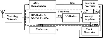
Figure 1 shows the internal structure of a passive RFID tag. It consists of an antenna and a tag IC. For very short-range distances, about 5–6 mm, an integrated multi-layer spiral inductor can be used for near-field coupling purposes. However, for long-range distances, of the order of several meters, the antenna must be designed off-chip to achieve sufficient gain and efficiency. The antenna and the NMOS rectifier must be matched in order to ensure maximum power is transferred between the two blocks. The tag IC includes three fully integrated parts: the VDD Generator circuit, the signal front-end (modulator/demodulator and the clock generator), and the digital part baseband processor. The principle of operation of the RFID tag can be described as follows. The rectifier converts the received RF power from the antenna into a sufficiently high DC voltage VR which is then further regulated by a voltage regulator to generate a stable voltage supply VDD to other blocks. The demodulator extracts the ASK signal and send it demodulated form to the baseband processor. The baseband processor manipulates the received data and then generates outputs according to the functions of the tag. Modulation is finally done by changing the effective impedance of the antenna to backscatter signals back to the reader. Usually, the rectifier used in RFID transponders consists of Schottky diodes and capacitors [Reference Balachandran and Barnett6–Reference Tran, Lee and Lee8]. Because of their small series resistance, low junction capacitance and low turn-on, Schottky diodes are widely used in rectifiers a lower loss in the substrate .To reduce the charge/discharge time and improve efficiency, they are however often not available in standard CMOS technology due to their unique device characteristics and manufacturing processes. This inevitably leads to a higher cost and thus affects their activity in rectifiers.
Passive UHF RFID tag diagram.

In this paper, we propose a new VDD generator for the UHF passive RFID tag. The block diagram of our proposed circuit is shown in Fig. 2. It consists of four sub-circuits: RF-limiter, NMOS rectifier, DC-limiter, and low-power regulator. The RF-limiter circuit limits the amplitude of the input RF voltage to prevent any damage to the rest of the circuit caused by the high-input power (breaking down of the transistors). The proposed NMOS rectifier produces a DC voltage from the amplitude of the input RF voltage. Its design is based on the use the diode-connected native NMOS transistor with ultralow-threshold voltage. Indeed the use of native NMOS transistor is less expensive and more compatible with standard CMOS technologies than Schottky diodes. The NMOS rectifier is fully integrable and takes advantage of both passive and active multiplications to reduce the required input power. The minimum required input power is −23 dBm to generate a 1.19 V supply voltage from a 50-Ω antenna at 900 MHz. Furthermore, due to the huge variety of the rectified voltage, we propose a new DC-limiter at the output of the NMOS rectifier. This DC-limiter clamps the output rectifier voltage to a narrower range. Finally, a new low-power regulator is proposed for regulating the supply voltage to a value of 1.19 V.
Block diagram of the proposed VDD generator.

The organization of this work is as follows. In Section II, theoretical analyses and design techniques of the proposed five stages NMOS rectifier RF–DC, for improving the stability and conversion efficiency, is presented. In Section III, a detailed description of the proposed RF-limiter is presented. The DC-limiter design is presented in Section IV. In Section V, the design of the low-power regulator is presented with details for low-voltage and low-power design considerations. In Section VI, the simulation results and layout of the VDD generator are presented. Finally, Section VII gives a summary and conclusion.
II. NMOS RECTIFIER
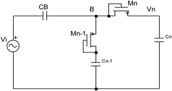
The NMOS rectifier circuit of a passive RFID tag converts the RF signal power to DC for power supply for all sub-circuits on the RFID tag. The initial unit voltage multiplying cell (UVMC) is shown in Fig. 4. The multiplying capacitor C n−1 can be seen as a DC-voltage source, and CB is an AC-coupling capacitor that conducts both input voltage V i and DC-bias voltage V n−1 on the following charging capacitor C n. Suppose V dn−1 is the voltage drop on NMOS FET M n−1, V dn for M n and VB is the DC voltage at point B, under steady-state conditions, we have
 $${V_B}={V_{n - 1}}+{V_i} - {V_{dn}}={V_n} - {V_i}+{V_{dn}}.$$
If W/L for M n and M n−1 is identical, then we have
 $${V_{dn}}={V_{dn - 1}} \Rightarrow {V_B}=\displaystyle{{{V_n}+{V_{n - 1}}} \over 2}.$$
The actual input signal for M n is V B + V i, due to the coupling capacitor CB. Suppose ΔV is the unit voltage increment, V d is the voltage drop on the transistor NMOS, namely,
 $$\Delta V={V_i} - {V_d} \Rightarrow {V_n}={V_{n - 1}}+2\Delta V.$$
If redefining a pair of native NMOS and capacitor as new UVMC, then the stage number in Fig. 3 becomes two, namely
 $${V_n}={V_{n - 2}}+2\Delta V\comma \;$$
where n = 2 K + 1, k is the number of UVMCs, equal to 1, 2, 3, … with the same Aspect ratio for all the native NMOS is the NMOS rectifier, every ΔV would be identical. Iterate the above formula, and we have
 $${V_n}={V_{n - 4}}+4\Delta V={V_{n - 6}}+6\Delta V.$$
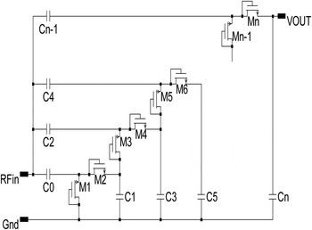
Schematic representation of the N-stage NMOS rectifier.

Initial unit voltage multiplying cell (stage).

Finally,
 $${V_n}=n\Delta V=n\lpar {V_i} - {V_d}\rpar \comma \;$$
where n is the number of native NMOS transistors and the circuit stage number. Equation (7) gives a mathematical expression for the proposed NMOS rectifier output voltage. In RFID applications, due to the lack of input power, the output voltage, and conversion efficiency of the NMOS rectifier are hence the two primary performance parameters. Be careful for the compromises that influence these parameters.
A) Matching network
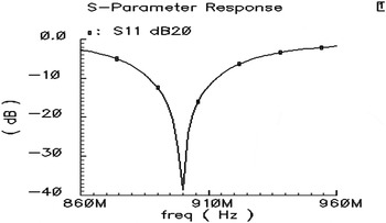
The matching network, which is usually off-chip, is used to match the tag chip's input impedance to the antenna for max power received; most of the simulations and the design work assume an antenna characteristic impedance of 50 Ω. This is based on the fact that most antennas have a standard 50-Ω characteristic impedance determined by experiments. However, for a general CMOS rectifier that has at its input capacitors linked in series, they usually carry large input impedance. Therefore, the transponder input impedance is mainly influenced by the rectifier. The S11 at the antenna is about −38.66 dB at 900 MHz which illustrates a good match, as shown in Fig. 5.
Input S11 as a function of frequency.

B) Output voltage
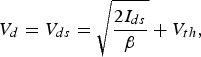
According to equation (7), the most obvious way to increase output voltage is to increase the number of stages and to minimize the voltage drop across the diodes V d. But, the increase the number of stages (UVMC) is subject to degradation of power dissipation and conversion efficiency, due to the short connection between the gate and drain of the all native NMOS transistors working in the saturation region,
 $${V_d}={V_{ds}}=\sqrt {\displaystyle{{2{I_{ds}}} \over \beta }}+{V_{th}}\comma \;$$
where β = μnCoxW/L [Reference Razavi9]. For a fixed output power, the average charging current for the CMOS rectifier is also constant. Obviously, for obtaining a higher output voltage with a constant output current I ds, a lower V d is desirable, that can be realized by a bigger W/L and/or a smaller V th.
C) Power conversion efficiency
The rectifier PCE is defined as
 $$PCE\lsqb \percnt \rsqb =\displaystyle{{{P_{out}}} \over {{P_{in}}}}=\left({1 - \displaystyle{{{p_{loss}}} \over {{p_{in}}}}} \right)\times 100\percnt \comma \;$$
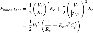
where P out is the output DC power of the rectifier and P in is the received RF input power, because of RF, the NMOS transistor in the rectifier is modeled as a channel resistance R c and a parasitic parallel capacitance C P. It has
 $${P_{nmos\comma loss}}=I_{ch}^2 {R_c}+I_{cp}^2 {R_c}\comma \;$$
where I ch and I cp are the average charging currents for R c and C P, respectively. Thus,
 $$\eqalign{{P_{nmos\comma loss}}& =\displaystyle{1 \over 2}{\left({\displaystyle{{{V_i}} \over {{R_c}}}} \right)^2}{R_c}+\displaystyle{1 \over 2}{\left({\displaystyle{{{V_i}} \over {\left\vert {{z_{cp}}} \right\vert }}} \right)^2}{R_c} \cr& =\displaystyle{1 \over 2}{V_i}^2 \left({\displaystyle{1 \over {{R_c}}}+{R_c}{\omega ^2}C_p^2 } \right).}$$
Note that P nmos,loss is smallest and PCE is largest when
 $${R_C}=\displaystyle{1 \over {gm}}=\displaystyle{{{V_{gs}} - {V_{{\rm th}}}} \over {2{I_{{\rm out}}}}}=\displaystyle{1 \over {\omega {C_P}}}.$$
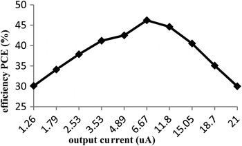
Accordingly, as shown in Fig. 6, there is a given output current that corresponds to the largest PCE.
Curve of efficiency versus output current.

III. RF-LIMITER
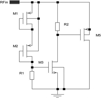
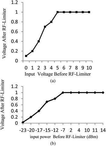
The input voltage of the RFID system can vary from several millivolts to tens of volts based on the distance between the reader and the transponder. In CMOS technology, the breakdown voltage of the MOS transistors is approximately 1–2.5 V with the 90 nm technology. The excessive voltage to the RF input of the tag could easily damage the chip structure. On the other hand, when the input voltage is large, the output voltage of the NMOS-rectifier circuit will have a large variation and the regulator design would be more challenging with the voltage overhead and the power consumption budget in hand. This shows the necessity of having an RF-clamping circuit that will limit the RF-input signal to approximately 1 V. Of course the voltage regulator can then stabilize this voltage to a desired value once the variation is limited. The schematic representation of the proposed RF-limiter circuit is shown in Fig. 7. Two diodes connected PMOS transistors are used to define the threshold voltage of the limiter. Once the input voltage exceeds the threshold voltage, M3 will be turned on. The gate voltage of M5 will approach 0 V causing VGS of M5 to approach VDD. The designed voltage clamp uses feedback to sense the input voltage at the RF port and to close the loop in such a way that the input voltage could not exceed 1 V. The M1 and M2 are low-threshold voltage PMOS transistors with a width of 0.5 µm, a length of 0.1 µm; M3 are low-threshold voltage NMOS transistors with a width of 3 µm; M5 NMOS transistors with a width of 10 µm, a length of 0.1 µm, and 14 fingers. The R1, R2 equals 1 kΩ. The voltage after using an RF-limiter circuit as a function of the amplitude of the input signal is shown in Fig. 8.
Schematic diagram of RF-limiter.

(a, b) input voltage after RF-limiter circuit.

IV. DC-LIMITER
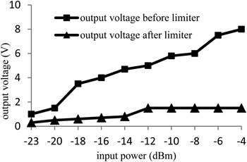
The output voltage of the NMOS rectifier depends on the RF input voltage so varies in a wide range. To limit the range of the changes in the output of the NMOS rectifier, a DC-limiter is used. During the low-power input, the limiter does not change the output of the NMOS rectifier. In the high RF energy periods, the limiter makes a bypass path for current and limits the output voltage to a certain value. The limiter bounds the rectifier output voltage variation to 1.5 V.
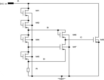
The proposed DC-limiter circuit for the NMOS rectifier is shown in Fig. 9. The circuit shown uses a specified fraction of the generated output voltage to control the gate voltage of transistor M3. This transistor acts very similar to a tunable load. The load current of the system is varied through the gate voltage that is set on the M3 transistor.
Schematic diagram of DC-limiter.

The size of the M5 is set to be larger than that of M7. This will lead to the fact that most of the current will choose the path that consists of transistor M5. This will result in the drain–source voltage of the transistor M6 to be smaller than that of the M4. Based on this analysis M7 will also work in the saturation region and therefore the voltage on node C will follow that of node B by a threshold voltage. If we neglect the substrate bias then we can safely say that the transistor M3 can be turned on when the voltage of node A goes above four threshold voltages. With the substrate bias, the turn-on voltage will even be higher. The M1, M2, M4, M6, and M7 are low-threshold voltage transistors with a 10-µm channel width and 0.1-µm channel length. The M5 is a low-threshold voltage transistor with a width of 5 µm and a length of 0.1 µm. The M3 is a low-threshold voltage transistor with a width of 25 µm, a length of 0.1 µm, and 10 fingers. The R is 10 kΩ.
As shown in Fig. 9, the voltages at nodes C and D can be described as follows:
 $$V\lpar C\rpar =V\lpar A\rpar - {V_{gs1}} - {V_{gs2}} - {V_{gs6}}=V\lpar A\rpar - 3{V_{gs1}}\comma \;$$
 $$V\lpar D\rpar =V\lpar A\rpar - {V_{gs1}} - {V_{gs2}} - {V_{gs4}} - {V_{gs5}}=V\lpar A\rpar - 4{V_{gs1}}\comma \;$$
 $$V\lpar D\rpar =I\lpar {M_1}\rpar R\comma \;$$
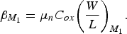
 $$I\lpar {M_1}\rpar =\displaystyle{1 \over 2}{\beta _{{M_1}}}{\lpar {V_{gs1}} - {V_{th}}\rpar ^2}\comma \;$$
where
 $${\beta _{{M_1}}}={\mu _n}{C_{ox}}{\left({\displaystyle{W \over L}} \right)_{{M_1}}}.$$
Using equations (14), (15), and (16), we can get theV gs1, which is given by
 $${V_{gs1}}={V_{th}} - \displaystyle{2 \over k}+\displaystyle{1 \over k}\sqrt {k\lsqb V\lpar A\rpar - 4{V_{th}}\rsqb +4}\comma \;$$
where k = (1/2)βM1R by equation (20) we can derive:
 $$\displaystyle{{\partial {V_{gs1}}} \over {\partial V\lpar A\rpar }}=\displaystyle{1 \over {2\sqrt {k\lsqb V\lpar A\rpar - 4{V_{th}}\rsqb +4} }}.$$
From equation (19), the resistor R acts as an attenuator besides limiting the current flow of the reference branch. Without this resistor, the gate–source voltage of M1 will be 1/4 of VA and also VC will follow VA with the ratio of l/4. Resistor R will attenuate the variation on the gate–source voltage of M1 that is caused by VA. When this attenuation is in place, VC can now follow VA with an effectively larger ratio. If we let R go toward infinity, then the gate–source voltage of M1 will remain almost constant and VC tends to follow VA. Therefore, given this analysis, once we look at this from a whole-circuit perspective, the attenuation on V gs1 looks very similar to again.
By equation (18), current of transistor M3 can be given by
 $$I\lpar {M_3}\rpar =\displaystyle{1 \over 2}{\beta _{M3}}{\left[{V\lpar A\rpar - 4{V_{th}} - \displaystyle{3 \over k}\sqrt {k\lsqb V\lpar A\rpar - 4{V_{th}}\rsqb +4}+\displaystyle{6 \over k}} \right]^2}.$$
Substitution with two limits of k, we can get
 $$I\lpar {M_3}\rpar =\displaystyle{1 \over 2}{\beta _{M3}}{\left[{\displaystyle{1 \over 4}V\lpar A\rpar - {V_{th}}} \right]^2}\comma \; \quad R=0\comma \;$$
 $$I\lpar {M_3}\rpar =\displaystyle{1 \over 2}{\beta _{M3}}{\left[{V\lpar A\rpar - 4{V_{th}}} \right]^2}\comma \; k=\displaystyle{1 \over 2}{\beta _{M1}}\comma \; \quad R=\infty.$$
After deciding the turn-on voltage of the limiter and the output voltage variation that can be tolerated, the size of transistor M3 can be found using equations (21) and (22); the sum output voltage at the output of the rectifiers before and after voltage limiter as a function of input power is shown in Fig. 10. The limiter circuit for the negative part of the rectifier is the same as for the positive one, but instead of using NMOS transistors, the effective same size PMOS transistors are used.
NMOS rectifier output voltage before and after using a DC-limiter as a function of input power.

A) Low-power regulator
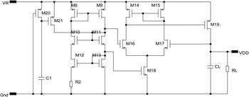
The regulator circuit comes after the DC-limiter. The regulator does two major functions. One is to regulate the output voltage to a preferred value and within a preferred range for passive UHF RFID. The other is to protect the inner circuits from breaking at high RF input power. The output of the voltage regulator will be used as the circuit's VDD voltage. The proposed regulator is shown in Fig. 11. This regulator consists of three blocks, a start-up with M20, M21, and C1. With gate connected to the earth, the M20 is always on. It leads to drain voltage of the M21 high voltage to avoid idle situation in the gates of M10 and M11, a reference voltage generator and regulator.
Schematic diagram of the low-power regulator.

Due to its passive and fully integrated characteristic, the RFID tag cannot have an external voltage reference. This means that all the reference voltages must be auto-generated, even the power supply voltage. As shown in Fig. 11, 1.2 V is generated directly by a reference self-biased voltage, instead of the conventional method for amplifying a low-precision reference voltage of the voltage pre-generated. M10–M13 build up a tow the cascade connection to increase the output resistance and all the transistors operate in the sub-threshold region of reduced power consumption.
In the threshold region in the drain–source [Reference Baker, Li and Boyce10] is almost
 $${I_{sds}}={I_{d0}}\displaystyle{W \over L}{e^{q\lpar {V_{gs}} - {V_{th}}\rpar /\lpar nkT\rpar }}.$$
If the W/L of M12 is made Q times larger than that of M13 and both have the same L, V gs of M12 and M13 can be rewritten in terms of the current I sds as
 $${V_{g{s_{12}}}}=n\displaystyle{{kT} \over q}\ln \displaystyle{{{I_{sds}}L} \over {{I_{d0}}QW}}+{V_{th}}\comma \;$$
 $${V_{g{s_{13}}}}=n\displaystyle{{kT} \over q}\ln \displaystyle{{{I_{sds}}L} \over {{I_{d0}}W}}+{V_{th}}.$$
Furthermore, we know that
 $${V_{g{s_{13}}}}={V_{g{s_{12}}}}+{I_{sds}}{R_2}.$$
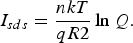
According to equations (23), (24), and (25), we have
 $${I_{sds}}=\displaystyle{{nkT} \over {qR2}}\ln Q.$$
This current is independent of the supply source DC, is smaller, than the current operation in a typical saturation region. The voltage on the drain of M11 can also be stable and independent of the power supply. Furthermore, to minimize the RF input power for the RFID tag, the voltage reference work under a power supply as low as possible is preferred, the current mirror load M8–M9 utilizes the low Vth PMOS FETs to reduce the requisite V ds voltage drops as well.
A low-power regulator is simply a differential amplifier with feedback. The feedback senses the output voltage and compares it with the V ref provided by the voltage reference of the second stage. For the differential amplifier, an NMOS amplifier is chosen with a PMOS active load. In order to achieve low-dropout regulation and ensure that M19 operates in the saturation region, the native MOS transistor with large W/L is used. CL is the loading capacitor. By multiplying of the NMOS rectifier and the regulating of a regulator, RF input of the tag is converted into a stable output, is independent the input, which can be used as the power supply for a passive UHF RFID tag with good efficiency.
V. SIMULATION RESULTS
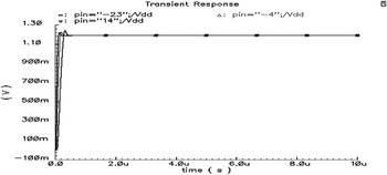
Figure 12 shows the simulation result of output voltage of proposed VDD generator with different input signals. Based on the practical design demands, the output needs to reach 1.19 V with a 1 MΩ load resistor. Our simulation shows that when input 900 MHz RF power changes from −23 to 14 dBm, the deviation of the output VDD from 1.19 V is less than 10 mV. In addition, with a −23 dBm input power, the obtainable largest conversion efficiency is still 26.96%, which is higher than the reported results in [Reference Qiang, Weining, Yin and Yude11–Reference Umeda, Yoshida, Sekine, Fujita, Suzuki and Otaka14] shown in Table 1. Considering the minimum required input power and the operating range of the different designs, Table 1 shows the efficiency of the proposed work compared to other works. These simulation results indicated that the presented novel VDD generator is capable to provide efficient, stable, and input-independent power supply for Passive UHF RFID tag.
Simulation results of the proposed VDD generator.

Comparison results.

*Normalized for 3 V generation **Normalized for 1.19 V generation *** Normalized for 4 W EIRP source.
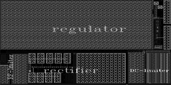
The proposed VDD generator was designed using 90 nm CMOS technology, 1 poly, 9 metal, The chip layout of the VDD generator is shown in Fig. 13, which includes the different sub-circuits such as an RF-limiter, NMOS rectifier, DC-limiter, voltage reference, and series regulator. The size of the whole chip is only 105 × 85 µm, which can be easily fitted into RFID tag. Meanwhile, it also provides a good compatibility with various digital and analog CMOS integrated circuits.
Complete proposed layout of VDD generator.

VI. CONCLUSION
This paper presents a novel VDD generator for a passive UHF RFID tag, consisting of an RF-limiter, NMOS rectifier, DC-limiter, and a regulator. Theoretical analyses and circuit simulations used for the design optimization is presented. The circuit demonstrates the capability of generating stable and input-independent DC voltages as the power supply for a UHF passive RFID tag. Using more stable and compatible MOS FET'S, the proposed circuits are hence more compatible with other CMOS circuits and can be used in a passive RFID tag.
 Smail Hassouni was born in Morocco, in 1985. He received B.S. and M.S. degrees in the Faculty of Sciences Dhar El Mehraz from Sidi Mohamed Ben Abdellah University in 2010 and 2011, respectively. Since 2011, He is currently working toward a Ph.D. degree at the same university. His interests are low-power circuit design techniques for RFID, RF front-ends for passive tags, and CMOS mixed-mode integrated circuit design.
 Hassan Qjidaa received his M.Sc. and Ph.D. degrees in Applied Physics from Claude Bernard University of Lyon France in1983 and 1987, respectively. He got the Pr. Degree in Electrical Engineering from Sidi Mohammed Ben Abdellah University, Fez, Morroco in 1999. He is now a Professor in the Department of Physics. His research interests include very-large-scale integration (VLSI) solution, image manuscripts recognition, cognitive science, image processing, computer graphics, pattern recognition, neural networks, human–machine interface, artificial intelligence, robotics, and so on.