I. INTRODUCTION
There is an increasing demand for high-data-rate wireless networks and the 60 GHz band is a good candidate for these applications. At 60 GHz band, a net data-rate of multi-gigabit per second can be achieved over short distances [Reference Smulders, Haibing and Akkermans1]. Examples of applications are wireless gigabit Ethernet [Reference Ohata2] or short-range wireless multimedia applications [Reference Smulders3]. Recently, with the emergence of low-cost CMOS technologies operating at millimeter wavelengths, fully integrated front-ends with low-directivity antennas on Silicon On Insulator (SOI) substrates have been studied intensively [Reference Barakat, Delaveaud and Ndagijimana4, Reference Barakat, Delaveaud and Ndagijimana5]. The size of such antennas is frequently smaller or of the order of 1 mm in dimension, and therefore is much smaller than modern probing devices. Thus, their radiation performance is difficult to characterize as they are perturbed by their testing environment such as radiofrequency (RF) probes, connecting bond wires and transmission lines (t-lines).
Several 3D radiation pattern measurement benches have been developed previously [Reference Zwick, Baks, Pfeiffer, Liu and Gaucher6–Reference Mohammadpour-Aghdam, Brebels, Enayati, Faraji-Dana, Vandenbosch and DeRaedt17]. The basic feeding technique uses an RF probe to have a direct contact with the on-chip antenna [Reference Zwick, Baks, Pfeiffer, Liu and Gaucher6–Reference Simons and Lee8]. However, as a standard probe device is much bigger and close to the AUT, it involves a limitation of the angular sector where measurements can be taken. Furthermore, it is metallic, which adds diffraction effects to the radiation pattern. To counteract this, a microwave absorbing material can be placed on the probe station metal surfaces. However, in view of the size of a probe, the absorber can cause even more masking effect on the radiation pattern. In [Reference Mohammadpour-Aghdam, Brebels, Enayati, Faraji-Dana, Vandenbosch and DeRaedt17], Mohammadpour-Aghdam et al. designed an antenna with contacts in the backside of the antenna's ground plane so that the RF probe did not alter the radiation pattern. However, this configuration is not applicable to most on-chip integrated antennas, which have the radiating element and the contact on the same metal layers.
One approach to improve the performance of these measurement techniques is to supply the AUT with a long feed line to extend the distance between the probe and the AUT. The feed line can be integrated into the same substrate as the AUT, as in [Reference Ranvier, Kyrö, Icheln, Luxey, Staraj and Vainikainen9, Reference Beer, Adamiuk and Zwick11], or it can be connected to the AUT via bond wires, as in [Reference Barakat18]. One advantage of using bond wires is that multiple AUTs can be connected to the same measuring apparatus. However, bond wires are difficult to handle at such high frequencies, because it is difficult to maintain a good impedance matching and the wires may trigger a parasitic radiation if they are too long. A V connector is generally used as an interface between the feed line and the instrumentation [Reference Ranvier, Kyrö, Icheln, Luxey, Staraj and Vainikainen9, Reference Barakat18], but the transition between this connector and the feed line has to be carefully controlled to guarantee a good impedance matching, and the connector can also mask a part of the desired scanning zone. Some authors have also tried to design a transition between the feed line and a waveguide in order to feed the antenna directly from a standard waveguide in the backside of the antenna, but this increases significantly the complexity of the design [Reference Yang, Chen, Huang, Wang and Wu19–Reference Hirokawa, Ando and Goto21].
This paper presents two novel techniques to feed integrated antennas with minimal parasitic scattering due to the antenna environment. The first method is based on customized RF probes that have been designed to increase the distance between the probe and the AUT. The second method is based on a t-line fabricated on a flexible substrate so that the RF connector can be located below the antenna ground plane. This article is organized as follows: Section II presents the AUT used in our measurement campaign, along with detailed simulated performances. Section III describes the measurement setup. Next, Sections IV and V present the two measurement techniques using customized RF probes or a flexible t-line, respectively. Experimental results are provided and compared to the simulation. Finally, Section VI presents the final conclusions.
II. AUT
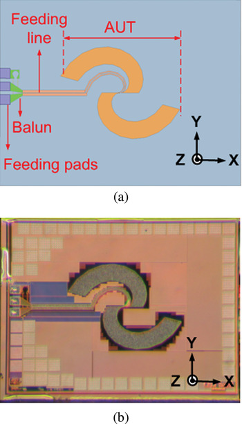
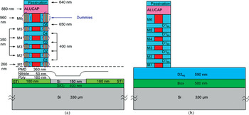
The AUT is a dual-arm Archimedean spiral integrated antenna realized on 130 nm CMOS SOI technology (Fig. 1) [Reference Barakat, Delaveaud and Ndagijimana5]. The antenna is fed through a 960 µm CoPlanar Stripline (CPS) reaching the edge of the chip, an integrated balun and the Ground-Signal-Ground pads. The two arms of the antenna are fabricated using the six (M1–M6) metal layers and the ALUCAP layer interconnected together with metal vias in the inter-metallic dielectric layers, reaching a total thickness of 5.75 µm to minimize resistive losses (Fig. 2(a)). The feeding line uses only the top (M6) metal layer and the ALUCAP layer with a total thickness of 1.84 µm in order to have a good control of its characteristic impedance. The antenna is surrounded by small dummy metallic squares in order to meet the metallic density requirements of the CMOS process. The silicon chip is 330 µm thick and glued onto a metallic plane acting as a reflector.
(a) Design of the AUT and (b) photograph of the AUT (size 2 × 1.5 × 0.33 mm3).

(a) Topology of the CMOS technology and (b) simulation model.

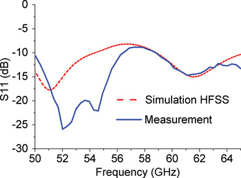
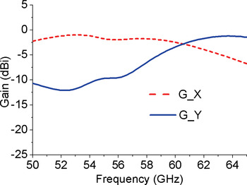
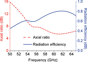
The simulation model is created using the software Ansys-HFSS (Fig. 2(b)). There are very large differences in scale between small metallic or dielectric structures and the whole chip, which can make a direct simulation of the chip impractical. Therefore, the dummies are not present in the simulation model and furthermore, some dielectric layers are merged into one equivalent layer. Figure 3 shows the simulated and measured reflection coefficient (S 11). This coefficient is measured with a standard probe (Infinity 67-A-GSG-100 supplied by CASCADE Microtech). It is a wideband antenna, operating in the 50–65 GHz range with a reflection coefficient below −8 dB for theoretical and experimental responses. A reasonable agreement between the theoretical and experimental responses is obtained, given the simplified model used to simulate the antenna with acceptable memory resources. The discrepancies below 58 GHz result from the simplification of the simulation model. Figure 4 shows the two simulated gain components as a function of frequency in the broadside direction. The maximum total gain is 0.36 dBi at 62 GHz. This AUT is elliptically polarized with an axial ratio higher than 5 dB across the bandwidth and a polarization direction rotating with frequency, i.e. the main polarization component is along X below 61 GHz and along Y above 61 GHz (Fig. 5). The simulated radiation efficiency is 81% at 62 GHz.
Simulated and measured reflection coefficient of the AUT.

Simulated gain in the broadside direction (θ = 0°) as a function of frequency.

Simulated axial ratio and radiation efficiency in the broadside direction (θ = 0°) as a function of frequency.

III. TEST BENCH
A) Radiation pattern measurement setup
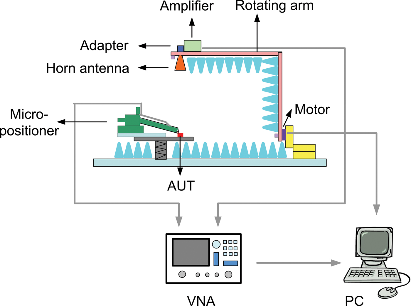
Figure 6 presents the test bench developed to measure the radiation pattern of the millimeter-wave antenna. This setup is attached on a honeycomb breadboard for isolation from external vibrations. The AUT is placed on a horizontal manually rotating chuck, while the measuring horn antenna is located at the end of a motorized rotating arm. This 20 dBi horn antenna rotates at a radius of 280 mm around the AUT. The AUT and the horn were accurately aligned using two lasers placed along the horn axis and the motor axis. The transmission coefficient (S 21) between the AUT and the horn antenna is measured by a Vector Network Analyzer (VNA) (Anritsu 37397C). The AUT is fed by a 90 cm coaxial cable and a 100 µm pitch ground–signal–ground (GSG) probe. The horn antenna is connected to a 30 dB amplifier through a waveguide-to-coaxial adapter and followed by a 90 cm flexible coaxial cable in order to ensure a smooth rotation of the arm. The rotating arm was made of Plexiglas (ɛr ≈ 3), and can be rotated in a ±120° range around the AUT. The appropriate polarization component is selected by a manual rotation of the horn antenna on the arm. Absorbing materials are used at any possible place(s) in order to minimize spurious reflections.
Schematic of the test bench.

B) Calibration
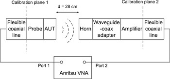
The VNA was calibrated with a Short-Open-Load-Thru (SOLT) coaxial calibration from 50 to 65 GHz. The calibration planes were set at the ends of the two flexible coaxial cables (Fig. 7). Therefore, the AUT gain has to be extracted from the measured transmission coefficient by taking into account the transmission gain/loss of each component (horn, amplifier, RF probe, and adapter) and the free space attenuation. Assuming a 0 dBi gain AUT, the transmission coefficient would be in the range of −13 to −10 dB. The average noise floor of the VNA was −85 dB. Thus, an excellent dynamic range of 73–76 dB is expected and considered as appropriate for the radiation pattern characterization.
Schematic of the measurement chain.

The radiation gain of the AUT was calculated by

where S21 is the transmission coefficient measured by the VNA, G Hom = 19.5 dBi is the gain of the horn antenna, G Amplifier = 27.5 dB is the gain of the amplifier, L Probe = 2.1 dB is the probe loss, L Adapter = 0.2 dB is the waveguide-to-coax adapter loss, λ = 5.08 mm is the wavelength and d = 28 cm is the distance between the AUT and the horn, all these numeric values are given at 59 GHz.
IV. PROBE FEED
Using an RF probe is a classical feeding technique to measure integrated antennas and circuits. Typically, a standard probe includes a 1 mm diameter coaxial line of 5–10 mm exposed length connected to a probe body of 2–3 cm. It is attached to a micro-positioner that is even bigger. One consequence of this technique is the masking effect caused by the probe body on a significant angular sector of the radiation pattern. Another consequence is the reflection and scattering effects of the waves radiated by the antenna on the body of the probe and positioner.
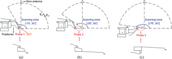
In this work, we have investigated and compared the performances of three RF probes in the V band. The first probe (Probe 1) is a standard probe (Infinity 67-A-GSG-100 supplied by CASCADE Microtech) having about 7 mm of coaxial length between the probe tip and the body (Fig. 8(a)). The two other probes are customized probes (Picoprobe 67A-GSG-100 supplied by GGB) exhibiting a 50 mm coaxial extension between the probe tip and the body. Of these two probes, one (Probe 2) has a regular connector position in the upward direction (Fig. 8(b)), while the other one (Probe 3) has a reversed connector position oriented in the downward direction (Fig. 8(c)). When using the latter probe with reversed body, we reversed the positioner as well so that the RF cable is placed underneath the AUT ground plane. These probes and their mounting configuration are represented in Fig. 8, showing also the expected scanning zone without the masking effect.
Measurement setup for the probe feed technique: (a) standard probe (Probe 1); (b) customized probe with 50 mm coaxial extension (Probe 2); and (c) customized probe with 50 mm coaxial extension and reversed connector (Probe 3).

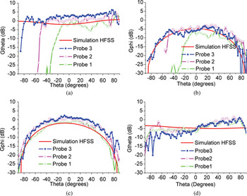
Figure 9 shows the theoretical gain radiation pattern of the AUT in the ZX and YZ planes at 59 GHz measured with the three probes. We performed each measurement several times and no significant measurement dispersion was observed. Figures 9(a) and 9(b) in the ZX plane containing the RF probe clearly show the extension of the scanning zone, i.e. angular sector with valid measurements, obtained with the customized probes, and thereby the reduction of the masked zone. Hence, the scanning zone extends approximately to [−10°, 90°], [−50°, 90°], and [−76°, 90°] with Probe 1, Probe 2, and Probe 3, respectively. Furthermore, smaller ripples and better agreement with the simulation results are obtained in the scanning zone with the customized probes. In the YZ plane, there is no masked zone, but the customized probes still managed to provide better measurement results in terms of ripple and gain level closer to the simulation.
Gain radiation patterns simulated and measured with the three RF probes: (a) ZX plane co-polarization; (b) ZX plane cross-polarization; (c) YZ plane co-polarization; and (d) YZ plane cross-polarization.

In order to analyze quantitatively the differences between the simulation and the measurements obtained with each probe in terms of a gain and ripples, we defined two figures of merit, namely the average gain error ΔḠ and the root-mean-square ripple R rms.
ΔḠ is defined as the difference between the mean values of the measured gain 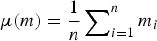 and the simulated gain
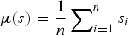 , where m i (resp. s i) are the measured (resp. simulated) gain values in the scanning zone where valid measurements are expected:

R rms is defined as the root-mean-square difference between the measured and simulated gain after removing the average gain error:
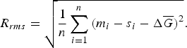
Table 1 compares the performances of the three probes for the co- and cross-polarization in the two principal planes. The coaxial extension of Probes 2 and 3 significantly reduces the masked zone in the ZX plane, and Probe 3 provides a minimum masked zone smaller than 15°, thanks to the reversed connector position. The average gain error ΔḠ is higher with Probes 2 and 3 than with Probe 1; we believe that this error is likely due to the calibration procedure rather than the probe themselves and further investigations are required to clarify this discrepancy. The ripples R rms are significantly reduced in the ZX plane, thanks to the extension of Probes 2 and 3, both for the co- and cross-polarization components, as expected. In the YZ plane, no significant difference is observed on the ripples obtained with the three probes; hence, the relative distance between the horn antenna and the probe does not change in this measurement plane, so that the fading effect is less visible.
Analysis of the measurement results with the three probes.

V. FLEXIBLE TRANSMISSION-LINE FEED
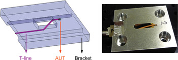
We introduce another feeding technique based on a microstrip t-line etched on a Kapton substrate. Kapton is a polyimide flexible film (ɛr = 3.4, tan δ = 0.009) which has the ability to withstand copper etching. In Fig. 10, the antenna chip is mounted on a metal bracket with a hole allowing the flexible t-line to go through the ground plane. One end of the flexible t-line is connected to the AUT, while the other end is connected to an end-launch V-band coaxial connector. This connection technique exhibits a low profile so that minor perturbations of the AUT radiation pattern are expected.
3D view and photograph of the AUT and the t-line mounted on a bracket.

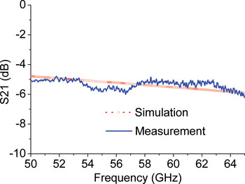
The flexible substrate is 42 mm long and 50 µm thick (Fig. 11(a)). The t-line has a width of 120 µm for 50 Ω impedances and a thickness of 18 µm copper on each side of the substrate. The other end of the t-line exhibits a microstrip-to-CPW transition to be connected to the chip pads (Ground-Signal-Ground). The contact is made using a wedge-bond technique similar to flip-chip with the two parts face-to-face as shown in Fig. 11(b). This technique avoids any bond wire suspended in the air that may produce parasitic radiation and mismatches. Furthermore, as the t-line is upside down, its parasitic radiation will not degrade with the AUT's radiation. Figure 12 shows the good agreement between the measured and simulated transmission loss of the t-line, which is close to 5.3 dB.
(a) Photograph of the flexible t-line on Kapton and (b) schematic of the connection.

Transmission coefficient of the t-line.

The gain values were calculated with the following equation taking additionally into account the t-line and connector losses:

where L Kapton ≈ 5.3 dB is the microstrip t-line loss and L Connector ≈ 1.25 dB is the connector insertion loss at 59 GHz.
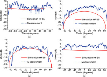
Figure 13 shows the gain measured in the ZX and YZ planes at 59 GHz. It shows that there is no more masked zone. The effective angular scanning sector achieved is [−90°, 90°], so that it is possible to cover the whole hemisphere with this method. The shape and average level of the measured co-polarization gain components in the ZX and YZ plane exhibit a good agreement with the simulation results. However, as shown in Table 2, substantial ripples are obtained, which are likely due to the scattering of the AUT radiation on the bracket. A possible solution would be to cover the bracket with a thin absorbing material. For the cross-polarization components, the gain is approximately 7 dB higher than the simulation results. The main difficulty and uncertainty in this measurement technique comes from the flip-chip connection that requires a highly accurate contact-pads alignment due to their small dimension and pitch. The dimensions of the GSG contact pads are 86 × 70 µm2 on the chip and 100 × 50 µm2 on the t-line both with a pitch of 100 µm. A small misalignment may lead to an asymmetric excitation of the two spiral arms. This uncertainty on the connection is currently under investigation, but may explain the discrepancies observed on the gain value and cross-polarization ratio.
Gain radiation patterns simulated and measured with the flexible t-line: (a) ZX plane co- polarization; (b) ZX plane cross-polarization; (c) YZ plane co-polarization; and (d) YZ plane cross-polarization.

Analysis of the measurement results with the flexible t-line feeding technique.

VI. CONCLUSION
This article presents a measurement setup for the characterization of low-directivity integrated millimeter-wave antennas. A 60 GHz spiral antenna integrated on a silicon chip is used as a test sample.
Two feeding techniques are investigated to interface the AUT and the instrumentation. The most straightforward technique is to use RF probes to directly connect to the antenna pads on the chip. In order to reduce the scattering and masking effect observed with standard probes, two customized probes have been experimented with a long coaxial extension between the probe body and the probe tips. These probes resulted in a significant improvement of the measured radiation patterns, and a good agreement with the simulations.
The second feeding technique is based on the use of a flexible t-line enabling the use of a standard V connector placed below the antenna's ground plane. The experimental results confirmed the absence of masking effect but further investigations are required to improve the accuracy of the radiation pattern.
ACKNOWLEDGEMENTS
This work was partially funded by the French National Research Agency under the project SIPCOM (ANR-08-NANO-048, programme Nanosciences – Nanotechnologies 2008).
 Yan Fu received M.S. and engineering degrees in radio frequencies electronics and optoelectronics from the Ecole Nationale Supérieure d'Electronique et de Radioélectricité de Grenoble, France, in 2008. She is currently working toward a Ph.D. degree in Joseph Fourier University (UJF). Her main research interest lies in characterization of integrated antennas at millimeter-wave frequencies.
 Laurent Dussopt received M.S. and Agrégation degrees in electrical engineering from the Ecole Normale Supérieure de Cachan, France, in 1994 and 1995, a Ph.D. degree in electrical engineering from the University of Nice-Sophia Antipolis, France, in 2000, and the “Habilitation à Diriger des Recherches” degree from the University Joseph Fourier, Grenoble, France, in 2008. From September 2000 to October 2002, he was a Research Fellow with The University of Michigan at Ann Arbor. Since 2003, he has been a Research Engineer at CEA-LETI, Grenoble, France. His research interests include reconfigurable antennas, millimeter-wave integrated antennas and antenna arrays, RF-MEMS devices and systems.
 Tan Phu Vuong (senior member IEEE) received a Ph.D. degree in Microwaves from Institut National Polytechnique (INP), Toulouse, France, in 1999 and an HDR (Habilitation à Dériger des Recherches) degree in Microwaves and Electronics from Institut Polytechnique de Grenoble (Grenoble INP), in 2007. From 2001 to 2008, he was an Associate Professor in microwave and wireless systems at the ESISAR high School for Engineers at Grenoble INP. Since 2008, he is Professor at Phelma High School for Engineers at Grenoble INP. His research interests include modeling of passive microwave and millimeter-wave integrated circuits. His current research interests include design of small antennas and printed antennas for mobile, RFID, as well as the design of passive and active millimeter-wave components.
 Fabien Ndagijimana is a Professor at Université Joseph Fourier in Grenoble, France. He received his Ph.D., specializing in Microwave and optoelectronics, in December 1990, at Institut National Polytechnique de Grenoble (INPG) in France. He then joined the faculty of Electrical Engineering ENSERG as an Associate Professor where he teaches microwave techniques and electromagnetic modeling. Since September 1997, he joined the Université Joseph Fourier of Grenoble, where he is a Professor at the Institut Universitaire de Technologie (IUT). His research activity in the Institut de Microélectronique d'Electromagnétisme et Photonique (IMEP-LAHC) focuses on the characterization and electromagnetic modeling of microwave and devices, and their integration on Silicon and SOI technologies for wireless radiofrequency applications. The actual research activity includes: integrated antennas for microwave and millimeter-wave applications, electrical characterization of associated material and substrates, and development of 3D electromagnetic simulation tools.