
Introduction
Thin films solar cells based on chalcopyrite Cu(In,Ga)Se2 (CIGS, η~21%) are great competitors to achieve the high-energy conversion efficiency of silicon devices (η~26% for a crystalline cell).[Reference Friedlmeier, Jackson, Bauer, Hariskos, Kiowski, Menner, Wuerz and Powalla1, Reference van Deelen and Frijters2] These copper-based ternary chalcogenides are among the promising materials to be applied as absorber layers in solar cells due to their low band gap,[Reference Lu, Jin, Liu, Guo, Liu, Liu, Cheng and Du3] high absorptivity coefficient into the visible and next infrared (IR) ranges,[Reference Yu, Kokenyesi, Keszler and Zunger4] high tolerance to defects and impurities and have been extensively studied during the last three decades.[Reference Ramanujam and Singh5, Reference Lee and Ebong6] However, efforts have been made about to seek new absorber materials to allow economical and scalable commercialization of chalcopyrite-based devices.
CuGaS2 is a wide band gap (2.40 eV) ternary chalcogenide,[Reference Han, Zhang, Zhang and Zeng7] isostructural to the CIGS and has relatively low toxicity.[Reference Jing, Wang, Zhu, Yao and Song8] The CuGaS2 is composed by elements more abundant than that chalcogenides based on In, Cd, Se, and Te: for example, (160 ppb) e Ga (16.9 ppm) e Se (0.05 ppm).[Reference Armaroli and Balzani9] However, the optimal band gap energy of a single band gap device was calculated to be approximately 1.4 eV according to the Shockley–Queisser limit. Although CuGaS2 has not suitable band gap to act as a light absorption layer in single junction solar cells, it is possible to modulate its band gap by intermediate band formation or lowering the band gap by metal doping. Experimental and theoretical studies have reported an increased optical absorption intensity of CuGaS2 doped with transition metals (Ti,[Reference Lv, Yang, Li, Li, Yi, Wang, Niu and Zhong10] Cr,[Reference Chen, Qin, Chen, Yang, Wang and Huang11] Ce,[Reference Xiao, Zhu, Ding, Wang, Fan and Bo12] and Fe[Reference Koskelo, Hashemi, Huotari and Hakala13]), post-transition (Sn[Reference Han, Zhang and Zeng14]), and 15 group elements (N, P, As, Sb),[Reference Han, Zhang, Zhang and Zeng7] in comparison with the undoped semiconductor.
The preparation of CuGaS2 thin films have been reported by several physical methods, for example, EBPVD (electron beam physical vapor deposition)[Reference Jeong and Park15] and MVPD (metalorganic vapor phase deposition),[Reference Kim, Park, Kim, Ok and Shim16] and spray pyrolysis.[Reference Hollingsworth, Banger, Jin, Harris, Cowen, Bohannan, Switzer, Buhro and Hepp17] These methods are relatively expensive due to the use of vacuum equipment and may present throughput limitations.
In this work, we present a solvothermal method to prepare bismuth (Bi)-doped CuGaS2 nanocrystals ink and we apply it to an all-solution-processed approach for the preparation of microcrystalline films with enhanced optical properties in comparison with the undoped semiconductor films. The low-cost deposition method is comprised by spray deposition of the chalcogenide nanocrystals ink onto the molybdenum (Mo) substrates. Besides, we also discuss the structure, composition, and optical properties of the metal-doped CuGaS2 films.
Experimental
Mo foil (0.1 mm, Sigma-Aldrich) was used as a substrate for all samples in this study. CuGaS2 and Bi-doped nanocrystals were prepared according to Chang et al.[Reference Chang, Chiu, Gao, Jheng and Tuan18] Briefly, to prepare Bi-doped chalcopyrite, CuCl (Sigma-Aldrich), Ga2(SO4)3. (Sigma-Aldrich), and Bi(NO3)3 (Sigma-Aldrich) (1:1:0.01, molar ratio Cu:Ga:Bi) were added to a three-neck flask containing oleylamine (Sigma-Aldrich). The mixture was heated up to 240 °C under vigorous stirring. Then, the reaction was started by the immediate injection of the solution of sulfur powder (Acros) in oleylamine, kept under stirring for 1 h, and allowed to cool to room temperature, afterward. The nanocrystals were washed, centrifuged, and redispersed in hexane.
Films were deposited by spraying the nanocrystals hexane solution (0.012 mg/mL) for 2 s on preheated 0.5 × 1.0 mm2 Mo foil substrates on a hotplate at 80 °C, and then it was repeated for 20 times, with intervals of 1 min for remaining solvent evaporation. Afterward, the films were annealed at 350 °C for 15 min to remove surfactant and remaining solvent, and at 500 °C for 1 h for improving crystallization under sulfur and nitrogen atmosphere to prevent decomposition of the material.
The composition and morphologies of the nanocrystals precursors and the CuGaS2 and Bi-doped CuGaS2 films were investigated by an EDAX (energy-dispersive x-ray analysis) and field-emission scanning electron microscopy (SEM-FEG, INSPECT F50) techniques. The organization at long distance of the chalcogenides was identified by x-ray diffraction (XRD) analysis performed with Cu Kα radiation (40 kV, 30 mA) using a Shimadzu model XRD 6000 diffractometer. The optical properties of the films were investigated by the UV–vis analysis measured between 300 and 2000 nm on a Cary 5 G Varian UV–vis–near-IR (NIR) spectrophotometer. X-ray photoelectron spectroscopy (XPS) measurements were performed on a Thermo Scientific K-Alpha spectrometer using monochromatic Al Kα (1486.6 eV) radiation.
Results and discussion
Bi-doped CuGaS2 nanocrystals
The ternary chalcogenides nanocrystals were prepared to be applied as building blocking to fabricate thin films using an all-solution processed method of deposition and avoid expensive techniques of vacuum.
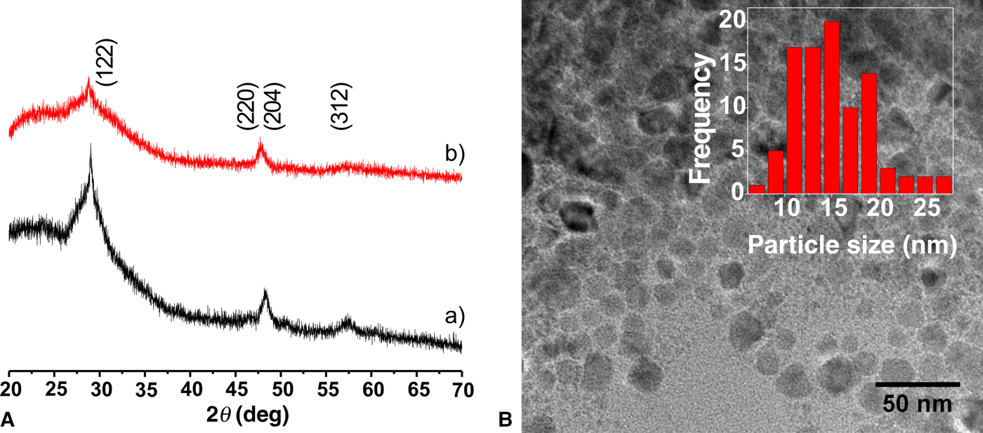
The x-ray diffractograms of the nanocrystals [Fig. 1(A)] show the main three peaks (112), (220)/(204), and (312) about 29, 48, and 57° 2θ,[Reference Chang, Chiu, Gao, Jheng and Tuan18] respectively, which correspond to the tetragonal chalcopyrite structure reported to CuGaS2 (JCPDS: 75-0103), with space group  $I\bar 42d$.[Reference Han, Zhang, Zhang and Zeng7] The broad peaks are characteristics of the nanometer-sized crystals of approximately 15 nm [Fig. 1(B)]. The peak (112) in Bi-doped CuGaS2 diffractogram shifts approximately 1° to lower 2θ degree in comparison with that for CuGaS2, which means that the incorporation of bismuth (Bi) into the chalcopyrite lattice promotes an increase of 0.3 Å in this interplanar distance. It may result from the that Bi atomic “radius” (1.48 Å) larger than that for Ga (1.22 Å).[Reference Cordero, Gómez, Platero-Prats, Revés, Echeverría, Cremades, Barragán and Alvarez19] Once identified the obtaining of Bi-doped CuGaS2 chalcopyrite nanocrystals, they were used fabricate thin films.
X-ray diffractograms of (A)—(a) CuGaS2 and (b) Bi-doped CuGaS2 nanocrystals, (B) Image of transmission electron microscopy (TEM) of Bi-doped nanocrystals, and a histogram of the distribution of particle size inset.

The effect of Bi-doped CuGaS2 on the structure and optical properties of thin films
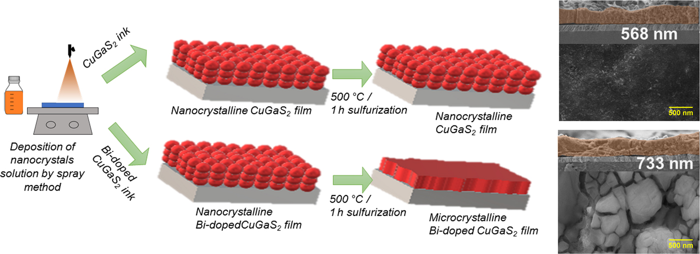
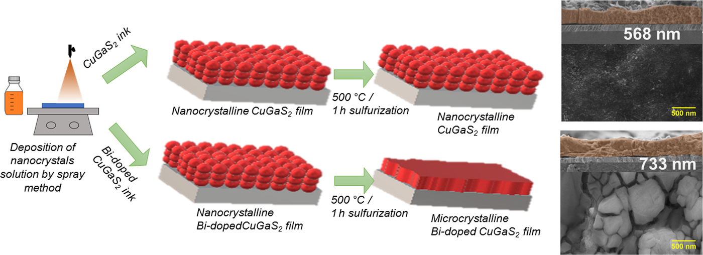
Figure 2 illustrates the procedure employed in this work to prepare microcrystalline thin films using nanocrystals as precursors. As already mentioned above in the experimental part, the CuGaS2 and Bi-doped CuGaS2 nanocrystals solution inks are spray-deposited on Mo foil, followed by annealing at 500 °C under sulfur atmosphere.
Scheme of microcrystalline bismuth-doped chalcopyrite thin-film preparation, and top view and cross-sectional SEM micrographs of CuGaS2 and Bi-doped CuGaS2 films.
An approximation of the stoichiometry of CuGaS2 and Bi-doped CuGaS2 films were determined by the energy-dispersive spectroscopy, presenting the atomic ratio equal to 1:1.02:2.13, and 1:0.96:0.04:2.10, respectively. It suggests that the composition of the Bi-doped material is CuGa0.96 Bi0.04S2.10, which is in agreement with the expected result.
Figure 2 also shows the top view and cross-sectional SEM images of the films after annealing. As observed, the film of CuGaS2 shows a surface formed by a packing of dense nanoparticles. On the other side, the films fabricated from Bi-doped CuGaS2 solution reveal a film comprised of notable grain growth, with particles size measuring from hundreds nanometer even up to approximate microns. Large grain-based films would decrease the density of deleterious grain boundaries in the direction of transport and enhance charge collection, in addition, the grain size is a parameter that determines series resistance, as well as, it would give higher conversion efficiency for solar cell applications.[Reference Guijarro, Prevot, Yu, Jeanbourquin, Bornoz, Bourée, Johnson, Le Formal and Sivula20] Bi-doped CuGaS2 crystalline film formed by larger grains present some cracks which can be attributed to a rapid solvent evaporation and during burning the long-chain surfactant.
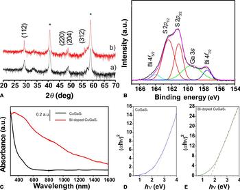
Figure 3(A) shows the diffractograms of the films prepared by spray deposition of nanocrystalline CuGaS2 and Bi-doped CuGaS2 inks. The diffractograms show two peaks at 41° and 59° 2θ attributed to the Mo substrates,[Reference Zhang, Ye, Liu, Chen, He, Liao, Han, Wang, Mei and Lau21] and the main three peaks corresponding to the chalcopyrite structure. There are no peaks related to CuBixSy, CuxS, or GaxS phases in the diffractograms confirming the purity of the films.
(A) X-ray diffractograms of the (a) CuGaS2 and (b) Bi-doped CuGaS2 films after sulfurization treatment at 500 °C, the peaks signed with * are attributed to Mo substrate. (B) X-ray photoelectron core-level spectrum for S 2p, Ga 3s, and Bi 4f, in Bi-doped CuGaS2 nanocrystals. (C) UV–vis–NIR spectra of the semiconductors. Panels (D) and (E) show the Tauc plots of CuGaS2 and Bi-doped CuGaS2 thin films.

The peaks attributed to CuGaS2 [Figs. 3(A, a)] are broader than those peaks in the diffractogram of Bi-doped CuGaS2 [Figs. 3(A, b)], which indicates that the Bi-CuGaS2 films are more crystalline than that undoped film. The crystallite size and growth were calculated using the Debye–Scherrer equation using the FWHM (full-width at half-maximum) of the (112) peak.[Reference Moreno, Ramirez and Gordillo Guzmán22] The diameter of the CuGaS2 nanocrystals was evaluated to be about 20 nm, and to Bi-doped CuGaS2 the diameters were estimated at approximately 500 nm. This result proves the coalescence of the precursors Bismuth-based nanocrystals into large grains.
In literature, it is reported many strategies to use grain growth promoters, such as Sb, Bi, and Mg, to obtain films with large crystallites originated from the coalescence of nanocrystals into large micro-sized grains during annealing. In the work reported by Guijarro et al.[Reference Guijarro, Prevot, Yu, Jeanbourquin, Bornoz, Bourée, Johnson, Le Formal and Sivula20] is reported the use of a solution of BiCl3 sprayed on the surface of CuGaS2, CuInS2, and CuGaInS2 films to promote the grain growth of the chalcopyrite particles. Although a little is known about the grain growth mechanism, it is already confirmed that microcrystalline metal-doped CuGaS2 films present significant enhancement in the carrier transport and collection of carriers. However, in this current work, we present a direct approach to deposit Bi-doped nanoparticles on the substrate, without further experimental step to metal doping the chalcogenide film. In addition, we ensure the distribution of Bi doping along all the film.
The incorporation of Bi into the chalcopyrite is confirmed by x-ray photoelectronic spectroscopy. Figure 3(B) shows a deconvoluted spectrum containing two peaks at 158.0 and 164.5 eV assigned to Bi 4f 7/2 and Bi 4f 5/2 in Bi-doped CuGaS2.[Reference Lee, Tan, Sumathi and Chai23] Additionally, the XPS spectrum shows the peaks attributed to S 2p 1/2 and S 2p 3/2 centered at 163 and 161.3 eV, attributed to the different binding with Ga and Cu, respectively, and a peak at 159 eV related to Ga 3s.[Reference Li, Zhao, Su, Hu, Yang and Zhang24]
Optical properties of CuGaS2 and Bi-doped CuGaS2 nanocrystals were analyzed using UV–vis–NIR spectroscopy. Figure 3(C) shows that the Bi-doped semiconductor film absorbs stronger in the visible and next IR region than the CuGaS2 nanocrystalline film. From the analysis of the Tauc plots [Figs. 3(D) and 3(E)], the values of the direct band gap of the chalcogenides are estimated in 2.3 eV to CuGaS2 and 1.7 eV to Bi-doped CuGaS2. The optical band gap of CuGaS2 prepared in this work coincides well with those typical tetragonal chalcopyrite reported in the literature, which is between 2.3 and 2.5 eV.[Reference Subbaramaiah and Raja25, Reference Ullah, Ullah, Bouhjar, Mollar and Marí26] The E g of Bi-doped film results in absorption at a wide range of the visible light spectrum and can increase the photon harvesting.[Reference Ullah, Ullah, Bouhjar, Mollar and Marí26] Similar results have been reported by Ti, V,[Reference Strandberg and Aguilera27] Cr,[Reference Ahsan, Kalainathan, Miyashita, Hoshii, Okada, Ahsan, Kalainathan, Miyashita, Hoshii and Characterization28] Ni,[Reference Han, Zhang and Zeng29] and Fe[Reference Aksenov, Kudo and Sato30] doping in chalcogenides. However, specifically considering to CuGaS2, there are several reports on Ti and Cr doping. Jing et al.[Reference Jing, Wang, Zhu, Yao and Song8] have shown the effect of the incorporation of Ti on the optical band gap of CuGaS2. The E g of Ti-doped CuGaS2 films reduced from 2.3 and 1.92 eV with increasing Ti concentrations. The incorporation of 2% of Cr into the mentioned chalcopyrite was reported by Chen et al.[Reference Chen, Qin, Chen, Yang, Wang and Huang11] The Cr doping resulted in a 1.85 eV band gap. Based on that, Bi doping has a more positive effect on the optical properties of the chalcogenide than the Ti and Cr, and its E g (1.7 eV) is closer to that optimal band gap energy of a single band gap device according to the Shockley–Queisser limit. According to the literature, the incorporation of metals in CuGaS2 would generate an intermediate band or decrease the band gap energy which can enhance absorption photons and allow these materials to be applied as a promising absorber layer in chalcogenides thin-film solar cells.[Reference Han, Zhang, Zhang and Zeng7, Reference Han, Zhang and Zeng29]
Conclusions
Bi-doped CuGaS2 chalcopyrite was synthesized via a simple solvothermal method producing 15.0 nm nanocrystals. The solution of these nanoparticles in hexane result in an ink which was deposited by spray onto Mo substrates. The Bi doping into CuGaS2 promoted a decreased band gap in comparison with the undoped chalcopyrite, broadening the spectral response and improving the light absorption in visible range. Moreover, the incorporation of Bi on CuGaS2 structure promoted grain growth producing microcrystalline films with particles of approximately 400 nm. The ability to improve growth control and quality of the grain structures, and the enhancement in the optical properties highlights Bi-doped CuGaS2 to be applied as an absorber layer in thin-film chalcogenides solar cells.
Acknowledgments
The authors thank Fundação de Amparo à Pesquisa no Estado de São Paulo, FAPESP (2013/07296-2, 2014/50249-8, and 2017/15144-9) for financial support to this work and Coordenação de Aperfeiçoamento de Pessoal de Nível Superior, CAPES/PNPD, for fellowship.