I. INTRODUCTION
A microstrip lowpass filter (LPF) with compact size and wide rejection band is a fundamental component in wireless communication systems to block unwanted signals and undesirable high-frequency harmonics. There are several configurations of microstrip lines that can be used as alternative structures for microstrip filter implementations [Reference Hong and Lancaster1]. Planar LPFs have been studied increasingly, because of compact size, low cost, simple structure, easy fabrication and integration. LPF design using conventional structures such as stepped impedance and open stubs are suffering from either spurious passband or poor cut off performance [Reference Karthikeyan and Kshetrimayum2]. A LPF using tapered compact microstrip resonator cell (T-CMRC) has been presented in [Reference Yousefzadeh and Hayati3], which has an ultra wide stopband, but it has a large circuit size. In [Reference Wu, Tseng and Tu4], a compact microstrip stepped impedance LPF using back-to-back C-shaped and triple C-shaped thin slots has been presented, which has wide stopband, but its frequency response is not sharp enough in the transition band and does not have good passband performance due to its significant insertion loss. A LPF using radial stub resonators is designed in [Reference Hayati, Majidifar and Sadeghi Fathabadi5] with wide and high attenuation stopband, but it has large size and a gradual transition band. A microstrip LPF that consists of reshaped rectangular dumbbell slots is designed in [Reference Mohra Ashraf6] with good insertion and return loss, but it is not compact and does not have sharp roll off and wide stopband. A LPF using circular hairpin resonators is designed in [Reference Yang, Xu, Zhao, Peng and Li7] with compact size, it does not have good insertion loss, sharp roll off and wide stopband. By cascading microstrip coupled-line hairpin unit, semi-circle defected ground structures and semi-circle stepped-impedance shunt stubs, a LPF is designed in [Reference Wei, Chen, Huang, Shi and Wang8], which suffers from large size, bad insertion and return loss and gradual transition band. A tap-connecting stepped impedance hairpin unit with two transmission zeros has been proposed for designing a LPF in [Reference Lin, Li and Mao9] that has good return loss, but it does not have compact size, good insertion loss and sharp transition band.
In this paper, a novel microstrip LPF with sharp transition band, wide stopband, good insertion loss and compact size using diamond-shaped resonator is designed. The proposed filter is simulated, fabricated and tested, where the measurement results are in good agreement with the simulation results.
II. FILTER DESIGN
The design process of the proposed filter has two steps, described below. The first step includes designing of the diamond-shaped resonator cell to achieve sharp transition band and second one designing of the suppressing cell and its addition to the proposed resonator to achieve wide stopband and eliminate the spurious harmonics.
A) Resonator design
Figure 1(a) illustrates a suitable lowpass prototype resonator for a three order elliptic function LPF with cutoff frequency 2.38 GHz and source and load impedance Z 0 = 50 Ω. The initial value of the LC circuit elements is obtained using the following equations [Reference Hong and Lancaster1]:
(a) An elliptic-function, lumped-element lowpass resonator. (b) Microstrip realization of the elliptic function lowpass resonator. (c) S-Parameters of prototype resonator.

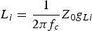 $$L_i = \displaystyle{1 \over {2\pi f_c }}Z_0 g_{Li} $$
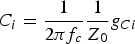 $$C_i = \displaystyle{1 \over {2\pi f_c }}\displaystyle{1 \over {Z_0 }}g_{Ci} $$
where f c is cut off frequency, Z 0 is characteristic impedance (50 Ω), g Li and g Ci are the inductive and capacitive elements, respectively. The calculated values of inductors and capacitors are as follows:
 $$L_{\rm 1} = {\rm 7}.{\rm 8}\, {\rm nH}\comma \; \, L_{\rm 2} = {\rm 1}.{\rm 54}\, {\rm nH}\comma \; \, L_{\rm 3} = {\rm 7}.{\rm 8}\, {\rm nH}\comma \; \, C_{\rm 2} = {\rm 1}.0{\rm 49}\, {\rm pF}$$
The microstrip LPF that is realized from the LC circuit is shown in Fig. 1(b). Initial physical lengths of the high and low impedance lines for realization of the desired L-C elements can be determined according to the design equations [Reference Hong and Lancaster1]:
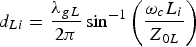 $$d_{Li} = \displaystyle{{\lambda _{gL} } \over {2\pi }}\sin ^{ - 1} \left({\displaystyle{{\omega _c L_i } \over {Z_{0L} }}} \right)$$
 $$d_{Ci} = \displaystyle{{\lambda _{gC} } \over {2\pi }}\sin ^{ - 1} \left({\omega _c Z_{0C} C_i } \right)$$
where λgL and λgC are the guided wavelength of high and low impedance lines, respectively, ωc is the angular cutoff frequency, Z 0C and Z 0L represent the impedance transmission lines with low and high impedance, respectively. The dimensions of the microstrip realization of the elliptic function lowpass resonator are: d L1 = 4 mm, d L2 = 2.2 mm, d C2 = 4.1 mm, d W1 = 0.1 mm, d W2 = 0.1 mm, and d W3 = 4.4 mm. The cutoff frequency can be specified in terms of the physical dimensions of the resonator as follows:
 $$f_C = \displaystyle{C \over {2\pi l_{Li} \sqrt {\varepsilon _{eff{\rm \lpar }L{\rm \rpar }} } }}\sin ^{ - 1} \left({\displaystyle{{\omega _c L_i } \over {Z_{0L} }}} \right)$$
 $$f_C = \displaystyle{C \over {2\pi l_{Ci} \sqrt {\varepsilon _{eff{\rm \lpar }C{\rm \rpar }} } }}\sin ^{ - 1} \left({\omega _c Z_{0C} C_i } \right)$$
where C is the speed of the light in free space, ɛ eff(L) and ɛ eff(C) are the effective dielectric constant. Figure 1(c) indicates the simulated S-Parameters of prototype resonator. As demonstrated in Fig. 1(c), the frequency response of prototype resonator has good transition band but it has bad insertion loss and return loss.
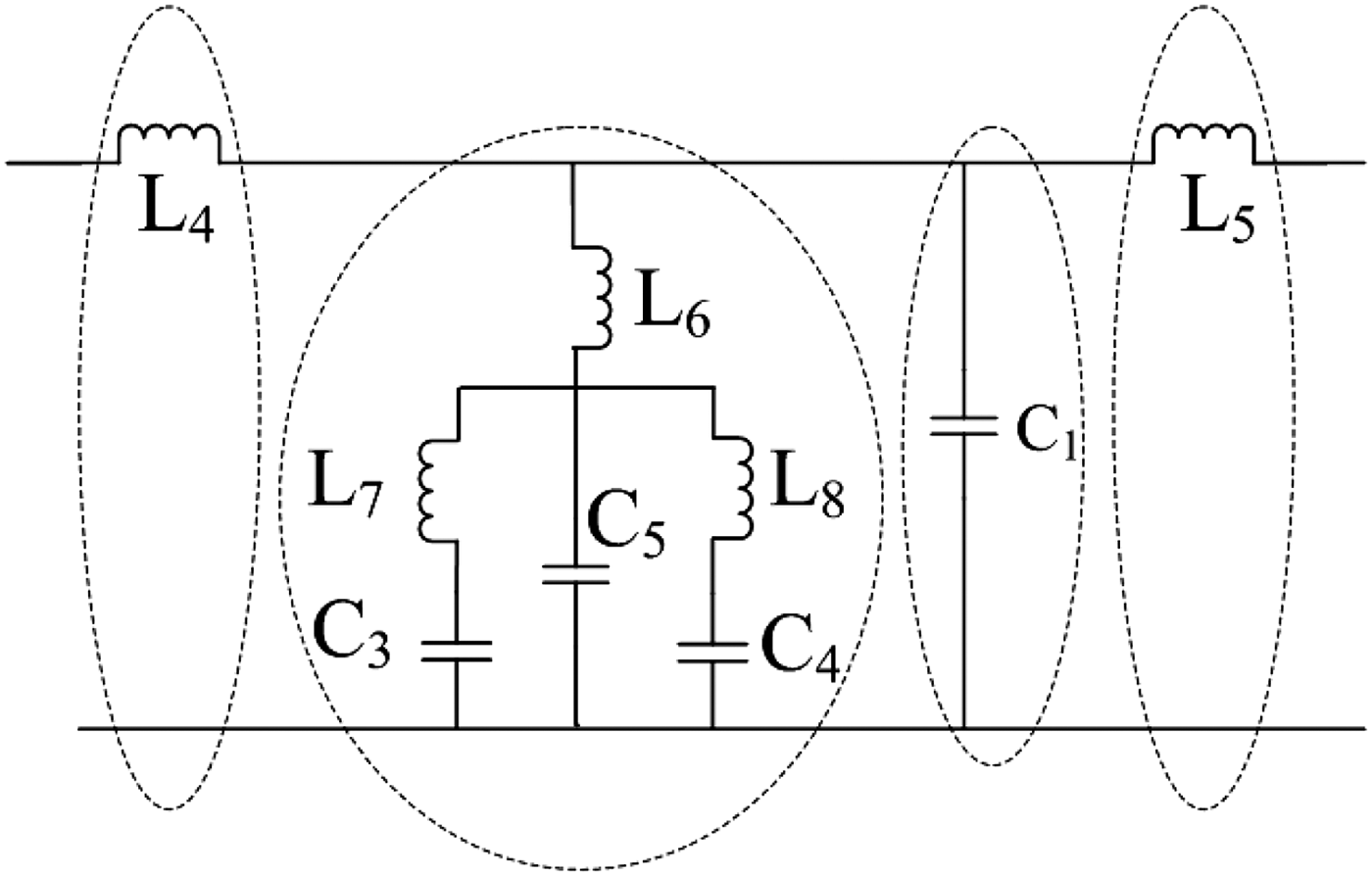
To achieve low insertion loss, good return loss and wide stopband the prototype resonator is modified to the triangular resonator with same area of the prototype resonator. Finally, to achieve sharp response, the tapered patch is loaded to the triangular resonator that creates diamond-shaped resonator as depicted in Fig. 2(a). The LC equivalent circuit of the proposed resonator is illustrated in Fig. 2(b). It shows that the triangular cell is composed of the two similar right-angled triangular patches. As illustrated in Fig. 2(b), L 7 and C 3 are the inductance and capacitance of the left triangular patch and L 8 and C 4 are the inductance and capacitance of the right triangular patch. C 5 and L 6 are the capacitance of the tapered patch and the inductance of the high transmission line, respectively. L 4 and L 5 are inductances of the transmission line between input and output ports. Also, C 1 is the capacitance created by bends with respect to the ground. Certainly to reach a suitable response, the final results are optimized by using the tune tools of an electromagnetic (EM) simulator of advanced design system (ADS) and the optimized values of the lumped-element proposed resonator are; C 1 = 120 fF, C 3 = C 4 = 0.59 pF, C 5 = 3 fF, L 4 = L 5 = 2.7 nH, L 6 = 2.2 nH, and L 7 = L 8 = 0.24 pH. Also the optimized dimensions of the proposed resonator are; L 1 = 6.3 mm, L 2 = 0.8 mm, L 3 = 0.1 mm, W 1 = 0.1 mm, W 2 = 2.2 mm, W 3 = 5.4 mm, W 4 = 0.6 mm, and L v = 4 mm. Figure 2(c) depicts the simulated S-Parameters of the proposed resonator. Also Fig. 2(d) shows the comparison between S-Parameters of prototype and proposed resonators and it is clear that the diamond-shaped resonator has the better response. In addition, as demonstrated in Fig. 2(e) the diamond resonator creates smaller transmission zero and causes sharper transition band, lower insertion loss and better return loss in comparison with the triangular resonator and these significant specifications imply the role of the tapered patch which is added to triangular resonator to propose a new microstrip resonator.
(a) Layout of proposed diamond-shaped resonator. (b) LC equivalent circuit of the proposed resonator. (c) S-Parameters of the diamond-shape. (d) Comparison between S-Parameters of prototype and proposed diamond-shaped resonators. (e) Comparison between S-Parameters of triangular and proposed resonators.
As indicated in Fig. 2(c), the −3 dB cutoff frequency of the proposed resonator is 2.34 GHz and it has one transmission zero near the passband in 3.09 GHz with the attenuation level of −52.28 dB. The insertion loss from DC to 2.13 GHz is less than 0.1 dB, which includes 91% of the passband width; also the return loss from DC to 1.7 GHz is better than 21.6 dB and the stopband width of the resonator is 7.26 GHz, from 2.67 to 9.93 GHz. Figure 3 shows that the LC circuit of proposed resonator can be divided into four networks, which are located in cascaded form, so the ABCD matrix of the proposed resonator can be obtained by [Reference Hong and Lancaster1]:
 $$\left[{\matrix{ A & B \cr C & D \cr } } \right]= \matrix{ {\matrix{ {\left[{\matrix{ 1 & {L_4 S} \cr 0 & 1 \cr } } \right]} & {\left[{\matrix{ 1 & 0 \cr Y & 1 \cr } } \right]} \cr } } & {\left[{\matrix{ 1 & 1 \cr {{1 / {C_1 s}}} & 0 \cr } } \right]} \cr } \matrix{ {\left[{\matrix{ 1 & {L_5 S} \cr 0 & 1 \cr } } \right]} \cr } $$
where in Fig. 3, L 4 = L 5 = L, L 7 = L 8 = L t, C 3 = C 4 = C t and the parameter “Y” in equation (7) is the admittance of two-port network belonging to second part in the LC circuit and can be calculated as follows:
 $$Y = \displaystyle{{C_5 \left({L_t C_t S^2 + 1} \right)+ 2C_t } \over {\left({C_5 \left({L_t C_t S^2 + 1} \right)+ 2C_t } \right)L_6 S + \left({L_t C_t S^2 + 1} \right)}} $$
Since C 5 ≪ C t; so the equation (8) is rewritten in the form of:
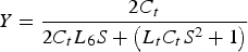 $$Y = \displaystyle{{2C_t } \over {2C_t L_6 S + \left({L_t C_t S^2 + 1} \right)}} $$
Therefore:
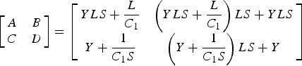 $$\left[{\matrix{ A & B \cr C & D \cr } } \right]= \left[{\matrix{ {YLS + \displaystyle{L \over {C_1 }}} & {\left({YLS + \displaystyle{L \over {C_1 }}} \right)LS + YLS} \cr {Y + \displaystyle{1 \over {C_1 S}}} & {\left({Y + \displaystyle{1 \over {C_1 S}}} \right)LS + Y} \cr } } \right]$$
Four cascaded networks of the proposed diamond-shaped resonator.
The S-Parameters based on the LC values of the proposed resonator are calculated using by the ABCD parameters as follows [Reference Hong and Lancaster1]:
 $$S_{11} = \displaystyle{{A + B/Z_0 - CZ_0 - D} \over {A + B/Z_0 + CZ_0 + D}} $$
 $$S_{21} = \displaystyle{2 \over {A + B/Z_0 + CZ_0 + D}} $$
So:
 $$S_{11} = \displaystyle{{S^2 \lpar \displaystyle{{YL^2 } \over {Z_0 }}\rpar + S\left[{YL\lpar Z_0 + \displaystyle{1 \over {Z_0 }} + 2\rpar + \displaystyle{{L^{_2 } } \over {C_1 Z_0 }}} \right]- \displaystyle{{LZ_0 } \over {C_1 }} + Y} \over {S^2 \lpar \displaystyle{{YL^2 } \over {Z_0 }}\rpar + S\left[{YL\lpar - Z_0 + \displaystyle{1 \over {Z_0 }}\rpar + \displaystyle{{L^{_2 } } \over {C_1 Z_0 }}} \right]+ \displaystyle{{L\lpar Z_0 + 2\rpar } \over {C_1 }} + Y}} $$
 $$S_{21} = \displaystyle{2 \over {S^2 \lpar \displaystyle{{YL^2 } \over {Z_0 }}\rpar + S\left[{YL\lpar - Z_0 + \displaystyle{1 \over {Z_0 }}\rpar + \displaystyle{{L^{_2 } } \over {C_1 Z_0 }}} \right]+ \displaystyle{{L\lpar Z_0 + 2\rpar } \over {C_1 }} + Y}} $$
Equations (13) and (14) show that the S-Parameters of the proposed resonator depend on C t, L and C 1, where these parameters are related to L 2,W 2 and W 3.
Figures 4(a–c) exhibit the simulated frequency response of the diamond-shaped resonator as function of L 2, W 2 and W 3, respectively. In Fig. 4(a), with increasing L 2 from 0.3 to 1.3 mm, the transmission zero move to lower frequency i.e., from 3.22 to 2.96 GHz, so the return loss changes from 18.5 to 22.9 dB, because of the increment of the capacitance of the tapered patch cell with respect to ground. (It should be mentioned although the coupling capacitance between the diamond-shaped patch cell and the transmission lines between input and output ports increases, but it has negligible effect on the proposed resonator). In Fig. 4(b), with increasing the length of W 2 from 1.2 to 3.2 mm, by increasing the inductance of the line and in order to decrease the coupling capacitance between the diamond-shaped patch cell and the transmission lines between input and output ports, the transmission zero closes to the cutoff frequency, significantly. In Fig. 4(c), with increasing W 3 from 4.4 to 6.4 mm the smaller transmission zero near the passband can be obtained, which leads to sharp frequency response. With respect to these variations and using an EM-simulator with gradient optimization tool (ADS), the optimized dimensions of the proposed resonator are obtained.
Simulated frequency response of proposed diamond-shaped resonator cell. (a) as function of L 2. (b) as function of W 2. (c) as function of W 3.
B) Suppressing cell design
To obtain a wider stopband region, we need to add a suppressing cell to the proposed resonator for eliminating high-frequency harmonics. Figure 5 shows two symmetrical C-shaped stubs as a suppressing cell, which has been added to the proposed resonator to eliminate undesirable signals in the stopband. As shown in Fig. 5, these stubs result in extra finite transmission zero within the stopband that suppress the harmonics and also extends the stopband.
Simulated frequency response of C-shaped stubs as suppressing cell.
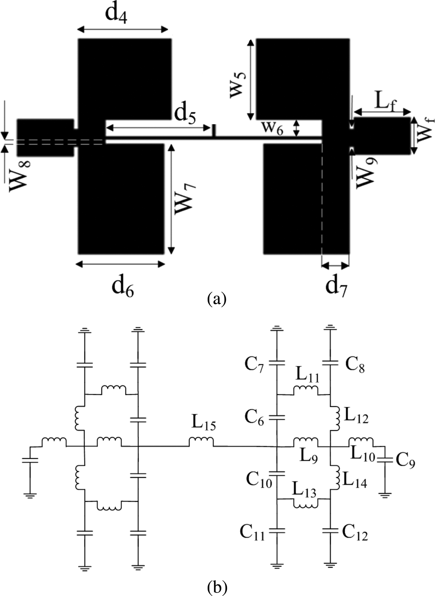
Figure 6(a) depicts the layout of the proposed suppressing cell and its L-C equivalent circuit is characterized in Fig. 6(b), which is obtained by using of methods, discussed in [Reference Hong and Lancaster1] and [Reference Hayati and Shama10]. In this LC circuit L 9 and L 15 are inductances of the transmission line between input and output ports. L 10 is inductance of the stub with widths of W 9. L 11 and L 13 depict inductances of the stubs with the length of d 4 and d 6. L 12 and L 14 are inductances of the rectangles with widths of d 4 and d 6. C 6 and C 10 illustrate the coupling capacitances between the transmission line between input/output ports and the rectangles with widths of d 4 and d 6, C 8 and C 12 are the capacitances created by bended lines with widths of W 6 and W 8, finally C 7 and C 11 are the capacitances of rectangle cells with widths of d 4 and d 6 with respect to the ground. The values of inductors and capacitors can be obtained by the equations (3) and (4). The optimized values of the lumped element circuit for C-shaped stubs are; L 9 = 1.58 nH, L 10 = 0.15 nH, L 11 = L 13 = 0.1 nH, L 12 = 0.5 nH, L 14 = 0.2 nH, L 15 = 5.6 nH, C 6 = C 10 = 10−8 fF, C 7 = 0.27 pF, C 8 = C 12 = 0.001 fF, C 9 = 17 fF, and C 11 = 0.26 pF. It is clear that the coupling effects are so negligible and can be ignored.
(a) Layout of the proposed suppressing cell L-C. (b) Equivalent circuit of the C-shaped stubs.
To improve bandwidth and sharpness, the resonator and suppressing cell section are combined. The layout of the proposed LPF is shown in Fig. 7(a). As illustrated in Fig. 7(b), the stopband width and sharpness of this LPF can be affected by the length of W 2. By increasing W 2, the coupling capacitance between the patch diamond-shaped cell and the suppressor unit will be attenuated. The optimized values are achieved using ADS software optimization tool, where W 2 is chosen as an important variable to obtain a wide stopband region. The optimized dimensions are as follows: W 5 = 3.3 mm, W 6 = 0.7 mm, W 7 = 4.5 mm, W 8 = 0.1 mm, W 9 = 0.7 mm, d 4 = 3.8 mm, d 5 = 4.4 mm, d 6 = 3.5 mm, and d 7 = 1.1 mm. Input/output ports are matched to 50 Ω using two stubs with dimensions of L f = 2.3 mm and W f = 1.5 mm. As illustrated in Fig. 7(c), the S-Parameters of LC simulation and EM simulation of the proposed LPF are in good agreement.
(a) The layout of the proposed filter, (b) simulated results of the proposed filter as function of W 2, (c) Comparison between S-Parameters of LC simulation and EM simulation of the proposed LPF.
III. MEASUREMENTS AND RESULTS
The designed LPF is fabricated on RT/Duroid 5880 substrate with the dielectric constant of 2.2, thickness of 20 mil and loss tangent of 0.0009 as illustrated in Fig. 8(a). The measurements are performed by the HP 8757A network analyzer. The simulated and measured S-Parameters of the proposed LPF are shown in Fig. 8(b), which indicates the −3 dB cutoff frequency of 2.6 GHz and the insertion loss less than 0.1 dB from DC to 2.52 GHz (96.9% of the passband region). It has one transmission zero near to the passband, which is located at 3.03 GHz with rejection level of −56.6 dB and two transmission pole that are located at 1.63 and 2.3 GHz with the attenuation levels of −47.03 and −55.94 dB, respectively. The stopband width is 17.95 GHz, from 2.89 to 20.84 GHz with the attenuation level better than −21 dB. The sharpness of frequency response is 0.288 GHz, from 2.606 to 2.894 GHz with the attenuation level of −3 and −20 dB, respectively. The physical size of the filter is 12.4 × 11.5 mm2. The group delay of the proposed LPF in the passband region is depicted in Fig. 8(c), which the maximum variation is less than 0.67 ns and it is so negligible.
(a) Photo of the fabricated LPF, (b) simulated and measured results of the proposed filter, (c) the group delay of the proposed LPF.
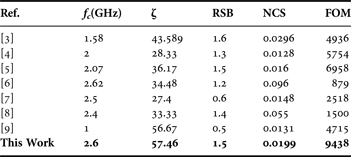
The performance of proposed LPF is compared with other published works in Table 1, where f c is −3 dB cutoff frequency and ζ is the roll-off rate that is used to evaluate the roll-off sharpness, which is defined as [Reference Wang, Xu, Zhao, Guo and Wu11]:
Performance comparison of the proposed LPF with other published works.
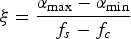 $$\xi = \displaystyle{{\alpha _{\max } - \alpha _{\min } } \over {f_s - f_c }} $$
where α max is the −20 dB attenuation point, α min is the −3 dB attenuation point, f s is the −20 dB stopband frequency and f c is the −3 dB cutoff frequency. The relative stopband bandwidth (RSB) is given by [Reference Hayati and Shama10]:
 $${\rm RSB = }\displaystyle{{{\rm stopband\lpar \!- 20}\, {\rm dB\rpar }} \over {{\rm stopband}\matrix{ {{\rm center}\matrix{ {{\rm frequency}} \cr } } \cr } }} $$
The suppression factor (SF) is based on the stopband suppression. A higher suppression degree in the stopband leads to a greater SF. For instance, if the stopband bandwidth is calculated under −20 dB restriction, then the SF is considered as 2. The normalized circuit size (NCS) is formulated as [Reference Hayati, Shama and Abbasi12]:
 $${\rm NCS} = \displaystyle{{{\rm physical}\matrix{ {{\rm size}\matrix{ {{\rm \lpar length}\matrix{ {{\rm \times }\matrix{ {{\rm width\rpar }} \cr } } \cr } } \cr } } \cr } } \over {\lambda _{\rm g} ^2 }} $$
This is used to measure the degree of miniaturization of a filter, where λ g is the guided wavelength at −3 dB cutoff frequency. The architecture factor (AF) can be identified as the circuit complexity factor, which is signed as 1 when the design is 2D and as 2 when the design is 3D. Finally, the figure-of-merit (FOM) is defined as [Reference Hayati, Shama and Abbasi12]:
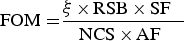 $${\rm FOM = }\displaystyle{{\xi \matrix{ {{\rm \times }\matrix{ {{\rm RSB}\matrix{ {{\rm \times }\matrix{ {{\rm SF}} \cr } } \cr } } \cr } } \cr } } \over {{\rm NCS}\matrix{ {{\rm \times }\matrix{ {{\rm AF}} \cr } } \cr } }} $$
According to Table 1, the proposed LPF has good RSB and also it has higher roll-off rate and FOM among the published works.
IV. CONCLUSION
A novel compact microstrip LPF is designed using diamond-shaped resonator. The most significant features of the proposed LPF are simple structure, wide stopband, sharp frequency response, good insertion loss, and low return loss in both stopband and passband region. The filter is simulated, fabricated, and tested. The measurement results are in good agreement with the simulation results. With the described characteristics, the proposed LPF is suitable for the modern communication systems.
Mohsen Hayati received the BE in electronics and communication engineering from Nagarjuna University, India, in 1985, and the ME and Ph.D. in electronics engineering from Delhi University, Delhi, India, in 1987 and 1992, respectively. He joined the Electrical Engineering Department, Razi University, Kermanshah, Iran, as an assistant professor in 1993. At present, he is an associate professor with the Electrical Engineering Department, Razi University. He has published more than 115 papers in international and domestic journals and conferences. His current research interests include a microwave and millimeter wave devices and circuits, application of computational intelligence, artificial neural networks, fuzzy systems, neuro-fuzzy systems, electronic circuit synthesis, modeling and simulations.
Mozhgan Amiri received the BE and ME in Electrical and Electronics Engineering, from Razi university, Kermanshah, Iran, in 2005 and 2013, respectively. Her current research interests include RF electronics microwave circuit design and modeling RFIC and MMIC.
Zahra Faramarzi received the BE and ME in Electrical and Electronics Engineering, from Razi university, Kermanshah, Iran, in 2005 and 2013, respectively. Her current research interests include design and optimization of microwave and RF circuits and MMIC.