I. INTRODUCTION
Since the beginning of dielectric resonator antennas [Reference Long, McAllister and Shen1], we have seen a fast evolution of dielectric resonator antenna (DRA) due to its favorable features such as compactness, light weight, wide impedance bandwidth, high gain, low profile, the ease of excitation, and the absence of conduction losses in the resonator. There are various feed mechanisms available for DRA [Reference Petosa2]. Among these, aperture coupling [Reference Martin, Antar, Kishk, Ittipiboon and Cuhaci3, Reference Chair, Lung, Yang, Kishk, Lee and Luk4] is one of the most versatile and efficient method as it provides physical isolation between the radiating structure and the feed. Among all conventional shapes, the rectangular dielectric resonator antenna (RDRA) offers more flexibility in design considerations [Reference Mongia and Ittipiboon5]. Hence, an aperture fed RDRA is chosen to be studied in this work.
To fulfill the increasing demands of compact and handy modern wireless communication systems, dual band and wideband antennas are well accepted by RF design engineers and researchers. Using a hybrid element has been a well-known method to achieve a dual frequency or a wideband performance. In [Reference Esselle and Bird6], a microstrip patch element on a truncated substrate is used to attain a wideband response. A DRA loaded with narrow parasitic conducting strips [Reference Hamad and Atallah7], and a combination of slot antenna and a DRA is exploited in [Reference Buerkle, Sarabandi and Mosallaei8] to increase the impedance bandwidth. In [Reference Ding and Leung9], a cavity with a zonal slot is used to introduce an additional band, but the low profile feature is divested. Two dielectric resonators are excited with the same slot in the ground plane [Reference Fan and Antar10], while in [Reference Gao, Ooi and Leong11] the authors have used a conducting loop to get an additional band. A radiating slot was used as the hybrid element to achieve the dual-band operation in [Reference Chen, Wang, Lin, Lin and Pan12, Reference Lin, Chen and Lin13]. In these designs, all hybrid elements are planar; hence the profile is retained. In most of these, the choice and the design of hybrid element are not articulate and simple. The authors of [Reference Chen, Wang, Lin, Lin and Pan12, Reference Lin, Chen and Lin13] have shown relations between slot dimensions and their corresponding resonant frequency. But, it is seen (in Fig. 3 of [Reference Chen, Wang, Lin, Lin and Pan12] and Fig. 4 of [Reference Lin, Chen and Lin13]) that the variation in one resonance is troubling the other resonance, which implies that they are not totally independent.
In this paper, a hybrid antenna is studied with two different and fully independent resonances. The RDRA is excited by a grounded slot at resonant frequency f DRA . Simultaneously an open half-wavelength microstrip resonator (MSR) is excited by the microstrip feed line at frequency f MSR . The most appealing merit is that the two radiators can be designed independently and operating frequencies f MSR and f DRA can be tuned just by varying the length and height of MSR and DRA, respectively. Moreover, the antenna is capable of tendering a reconfigurable dual-band or a wideband (both the modes are merged together) operation by choosing either MSR or DRA or both electronically. Some initial results have been reported in [Reference Gupta and Parihar14].
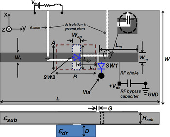
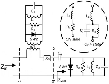
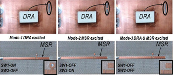
Additionally, a reconfigurable operation is proposed with three modes; mode 1 (only DRA is excited), mode 2 (only MSR is excited), and the mode 3 (hybrid, both are excited). Modes 1–3 state three different bias states of two PIN diodes shown in Fig. 1. As per system requirement any desired mode could be obtained by simply applying different bias voltages to the two PIN diodes. An equivalent circuit model for the proposed hybrid antenna is extracted and validated with three-dimensional (3D) electromagnetic (EM) model. The proposed circuit (Fig. 2) has been studied with actual diodes and biasing circuitry with the help of CST MW Studio and ADS. To validate the results, multiple circuits with ideal switches (a metallic strip is used in the ON state and removed in the OFF state) are fabricated and tested. Although this introduces significant errors, the principle of operation is verified.
Top and side views of the reconfigurable hybrid DRA with HPND-4005 diodes and the biasing scheme. Inset depicts biasing capacitor in ground slits.

Equivalent model of the proposed hybrid DRA. R 1 = 50 Ω, L 1 = 0.146 nH, C 1 = 3.74 pF, R 2 = 6 kΩ, L 2 = 1.37 nH, C 2 = 0.3 pF, and C g = 0.0415 pF. Inset shows ON and OFF states equivalent of a pin diode.

II. RECONFIGURABLE ANTENNA DESIGN
The proposed hybrid DRA is shown in Fig. 1. It consists of a basic RDRA and an open ended microstrip line resonator (MSR) on back side. The RDRA is fed by an aperture/slot coupled 50 Ω microstrip feed line which is printed on a substrate of relative permittivity ε
sub
= 3.2, and a thickness of H
sub
= 0.762 mm. The ground plane has a length of L = 50 mm and a width of W = 25 mm. The 50 Ω line has a width of W
f
= 1.8 mm. The optimized area of the aperture is L
ap
× W
ap
(7 × 1.1 mm2). For maximum coupling, the aperture and the RDRA are kept concentric. The RDRA has a dimension of A × B × D (7 × 15 × 5 mm3) and a relative permittivity of ε
dr
= 10.2. The RDRA is excited in
 $TE_{\delta 11}^x $
mode and its resonant frequency can be determined using following transcendental equation, [Reference Petosa2]:
 $$k_x \tan ({{k_x A} / 2}) = \sqrt {\left( {\varepsilon _{dr} - 1} \right)k_0^2 - k_x^2}, $$
 $$k_x^2 + k_y^2 + k_z^2 = \varepsilon _{dr} k_0^2, $$
where
 $$k_y = \displaystyle{\pi \over B}{\rm,} \quad {\rm} k_z = \displaystyle{\pi \over D},\quad {\rm and}\quad {\rm} k_0 = \displaystyle{{2\pi} \over {\lambda _0}}. $$
The k 0 is the free space wave number. For the above-mentioned RDRA, the resonant frequency is calculated as f DRA = 6.75 GHz. An open stub matching section of length L s = 6.4 mm is extended from the center of the aperture to nullify the susceptance provided by the aperture. Then, a very simple and planar λ/2 (at different frequency f MSR ) MSR patch is integrated for dual/wideband operation. The MSR has a width of W m = 1.8 mm, and a length of L m = 12 mm. The MSR is capacitively coupled to the open stub matching section through a gap of G = 0.2 mm. To achieve the agility in frequency two switches SW1 and SW2 (shown in blue, Fig. 1) are used. To control the MSR's resonance, switch SW1 is used between the MSR and the ground through via hole. If it is ON, then the MSR will not take part in the radiation; but in its OFF state, the MSR will resonate at f MSR = 7.2 GHz (in this work). Another switch SW2 is used to enable/disable the DRA excitation at the desirable frequency band. The resonant length of the MSR is calculated by (3) using effective permittivity,
 $$L_m = \displaystyle{c \over {2f_{MSR} \sqrt {\varepsilon _{sub\_eff}}}} - 2\Delta l,$$
where c is the velocity of light and ∆l is the end correction length due to fringing field lines [Reference Kirschning, Jansen and Koster15].
A) The biasing scheme
To control the two PIN diodes, a biasing scheme is also proposed in Fig. 1 and same has been used in ADS simulations. For diode SW1 the dc supply is given through an inductor placed at the center of the MSR (E-field minimum point), realized by a thin printed line of quarter wavelength at f MSR . The inductor is working as a RF choke and terminated with a capacitor to isolate the RF and the DC source. To bias the switch SW2, two narrow slits (0.1 mm) for dc isolation have been made in the ground plane. The slits are introduced transversely to the aperture's magnetic field causing minimum field disturbance. Two capacitors of 50 pF are used to provide low impedance for RF. The spurious resonant behavior of the ground slits may be avoided by appropriately choosing the position of the capacitors, in the desired frequency band. The forward bias current of 120 mA is used to activate the PIN diode and zero bias voltage to make the diode in OFF state. Avago HPND-4005 PIN-diode with SPICE parameters: I r = 100 nA, R s = 5 Ω, C j = 0.017 pF, V f = 1 V, and V br = 120 V is used as a switching device in ADS simulations with complete biasing circuit. However, in fabricated circuit, ON/OFF state is realized by the presence/absence of a small (1.1 × 0.5 mm2) metal strip.
B) Equivalent circuit model
An equivalent circuit for the proposed antenna is demonstrated in Fig. 2. The DRA is modeled as a low Q parallel resonant network, comprised of R 1, L 1, and C 1, using the methods given in [Reference Ain, Qasaymeh, Ahmad, Zakariya and Ubaid16, Reference Collin17]. The magnetic coupling to the DRA is replaced by a transformer of n:1 turns ratio, which decides the amount of coupling between the feed line and the resonant circuit. An additional series reactance X s = −jZ 0cot (βl) is caused by the λ/4 open stub termination of the transmission line. The gap between open stub matching section and MSR is approximately realized by a series capacitor C g [Reference Kirschning18]. The open-ended MSR is replaced by its lumped equivalent; initial values of R 2, L 2, and C 2 can be found using the equations given in [Reference Pozar19]. The parameters L 2 and C 2 were optimized to achieve the desired impedance bandwidth. The simulated Q factor is used to calculate the lumped element values and is given as Q = ( BW√2)−1, where BW is the −10 dB impedance bandwidth of MSR obtained from full-wave EM simulation. The circuit in Fig. 2 has been simulated in a high-frequency circuit simulator, ADS-2014. The results obtained in ADS are close to those obtained in a full-wave EM simulator and the error is limited within 3%. Two switches (diodes) SW1 and SW2 also are depicted to control operation of the two radiators. In Fig. 2, the inset shows the typical equivalent circuits (the values of L p = 0.1 nH and R p = 15 kΩ have been considered in this work) of the diode in ON and OFF states which may be substituted accordingly.
III. PARAMETRIC STUDY
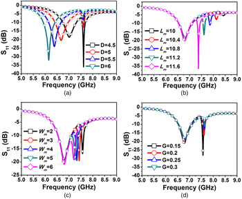
A detailed sensitivity analysis has been carried out and shown in Fig. 3, to explore the variations in antenna's characteristics from optimized values. DRA's height (D) shows an inherent downward trend in its resonant frequency and it is not unusual. In Fig. 3(a), the resonant frequency variation of DRA is shown with change in the DRA's height (D). As expected the MSR's resonant frequency is found unaffected.
Parametric study with: (a) height of the DRA, D, (b) length of the MSR, L m , (c) width of the MSR, W m , and (d) microstrip gap, G. All dimensions are in mm.

Most importantly, there are two critical parameters which influence the antenna's performance considerably. First one is the length of the MSR; L m . Figure 3(b) shows the simulated resonant frequencies (f MSR ) for different values of L m . It is noticed that the DRA mode is intact and independent of the MSR mode. The effect of the width of the MSR (W m ) has been investigated in Fig. 3(c). The resonant frequency (f MSR ) drops for an increment in the MSR dimensions. A small width of the MSR results into a narrow bandwidth. Another dimension in this design which should be chosen deliberately is the microstrip gap (G). This gap acts as an impedance matching element between the feed line and the MSR. A suitable gap mitigates the inductive reactance of the MSR at the resonant frequency. In reference to Fig. 2,
 $$Z_{in}^{2 - 2^{\prime}} = Z_{MSR} - jX_C = Z_0, $$
where X c is the reactance of the gap capacitance C g at f = f MSR . The effect of variation in the gap dimension, G has been demonstrated in Fig. 3(d). It is clear that while changing G the impedance matching of MSR is changed which is well expected.
IV. RESULTS AND DISCUSSION
A) Simulation results
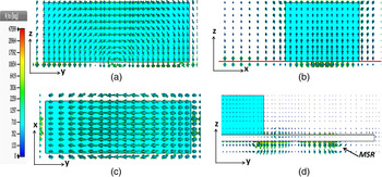
The E-field distribution is shown in different planes in Figs 4(a)–4(c); the E-field inside the DRA matches to the fundamental mode of RDRA which identified as
 $TE_{\delta 11}^x $
and Fig. 4(d) substantiate that the MSR is radiating in fundamental mode
 $TM_{010}^z $
at its resonant frequency. Further, surface current distribution is also studied in Fig. 5. When SW1 is ON (metal strip is present) and SW2 is OFF (metal strip is removed), no current is flowing through the MSR (Fig. 5(a)) and it is inactive while in ground plane current is surrounded to the aperture causing a strong magnetic field across it which makes the DRA active. In second case, when SW2 is ON and the SW1 is OFF (Fig. 5(b)), the aperture gets shorted and allows the current to pass through it consequently DRA becomes inactive. In this case, the current exists into the MSR resulting into
 $TM_{010}^z $
radiation at f
MSR
. At last, the current is distributed along the MSR as well as the aperture in Fig. 5(c), which confirms that both are active and radiating.
E-field distribution in: (a) the y–z plane, (b) the z–x plane, (c) the x–y plane in DRA at 6.75 GHz, and (d) in the y–z plane in MSR at 7.25 GHz.

Surface current distribution: (a) at 6.75 GHz when SW1 is ON, (b) at 7.25 GHz when SW2 is ON, (c) at 7 GHz when both the switches are OFF.

From the previous section, it is apparent that the two modes (DRA & MSR) are fully independent and can be designed separately. The DRA mode is not bothered when the MSR resonant length is changed; a decrease in resonant frequency (f MSR ) in accord with equation (3) has been seen when the length (L m ) is increased. Similarly a downward trend is shown in DRA's resonant frequency f DRA , when the DRA height (D) is increased. A good matching for MSR (mode 2) can be achieved by optimizing the microstrip gap (G) as shown in Fig. 3. For increasing W m , the MSR's resonant frequency (f MSR ) is getting downshifted due to varying C g (Fig. 2). As the width of the MSR increases the gap capacitance is also increased and the resonant frequency of the MSR is controlled by the total capacitance given by equation (5).
 $$f_{MSR} \propto \displaystyle{1 \over {\sqrt {(C_g + C_2 )}}}. $$
In this design, a hybrid element, the MSR is chosen which offers an advantage. By choosing wisely, the either dimension of the MSR (L m and W m ), a dual-band or a wideband operation can be accomplished.
B) Measured results
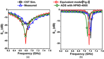
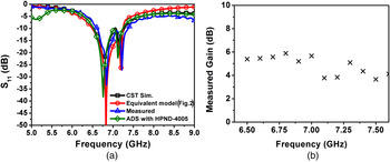
Based on the systematic parametric study carried out in Section III, optimized dimensions are obtained as given in Section II, and used to fabricate the prototypes for a reconfigurable dual-band and/or wideband operations. In Fig. 6, measured reflection coefficients of modes 1 and 2 (reconfigurable dual-band operation) are compared with simulation results obtained from: (1) full-wave EM simulation (CST) for the geometry shown in Fig. 1 without biasing circuit (with ideal switch), (2) ADS for equivalent circuit model in Fig. 2 (with ideal switch), and (3) ADS using actual diode models and complete biasing circuitry as shown in Fig. 1. It is clear that they are in well agreement for both the modes. A downshift is seen in f MSR (green line in Fig. 6(b)), when the diode model is used. This is caused by the additional off-state capacitance (C j ) of diode SW1 which is added with C 2 in equation (5). The minor shift in the measured results of Mode 1 is caused by the extra corroding of the DRA. The obtained impedance bandwidth is 60 and 600 MHz for the MSR and DRA modes, respectively. The measured and simulated reflection coefficients of the prototype for wideband operation (mode-3) are shown in Fig. 7(a). It is shown that it provides a bandwidth of 760 MHz in the range of 6.62–7.38 GHz which is higher by 700 MHz than to the MSR mode and 160 MHz from DRA mode. The wideband antenna shows about 11% bandwidth at 7 GHz.
Reflection coefficients for the two individual modes: (a) mode 1, SW1 “ON” and SW2 “OFF”, (b) mode-2, SW1 “OFF” and SW2 “ON”.

(a) Reflection coefficient variation for the prototype wideband hybrid DRA (Mode 3). (b) Gain of the antenna in wideband mode.

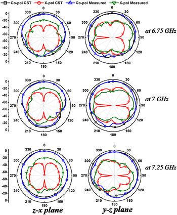
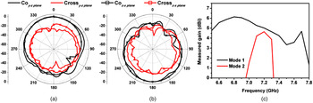
The measurements of radiation patterns for all the three modes have been carried out. The patterns for wideband operation (mode 3) in different planes at different frequencies are shown in Fig. 8. It is depicted that the antenna shows a broadside radiation over the band. At the upper frequency a significant back radiation is observed, which is expected the way MSR is positioned. A very low, <−15 dB X-polarization is measured in the broadside direction all over the impedance bandwidth. In Fig. 7(b), gain of the antenna is shown and measured gain ranges between 5.8 and 3.7 dB in the spectrum of 6.6–7.4 GHz. The far-field patterns for the DRA mode (mode 1) and the MSR mode (mode 2) have also been measured and are depicted in Fig. 9. It is confirmed that both the radiators are functioning in their respective fundamental modes. In mode 2, the maxima is observed at θ = 180° which is very obvious the way MSR placed. Figure 9(c) displays the measured peak gain in modes 1 and 2. A study has been done and included in Fig. 10 to learn the insertion loss and isolation characteristics of the diode in ON and OFF states, respectively. It is realized that in each mode the OFF diode is providing an isolation of more than 20 dB, which corroborates that the all three modes can be utilized independently. Figure 11 shows three different fabricated prototypes to realize the three reconfigurable modes of operation.
Far-field power patterns of the prototype antenna in wideband mode.

(a) Measured far-field patterns in mode 1 at 6.75 GHz, (b) in mode 2 at 7.2 GHz, and (c) measured gain.

Isolation study of diodes in OFF state: (a) mode 1, (b) mode 2, and (c) mode 3.

Photographs of the fabricated prototype antennas (top and bottom views) with ideal switches, inset shows SW2 beneath the DRA block and expanded view of SW1.

V. CONCLUSION
A reconfigurable dual/wideband hybrid DRA has been implemented and tested experimentally. An adequately accurate electrical equivalent of the hybrid antenna is tendered. A parametric analysis has been carried out to understand the antenna behavior. The two modes (DRA & MSR) are found totally independent and can be used for a reconfigurable frequency band operation and for wideband operation by merging them electronically. The fabricated reconfigurable prototypes are tested for all three modes. In the wideband mode, it shows a bandwidth of 11% and a compact size of 0.58λ 0 × 1.16λ 0 at 7 GHz. The antenna shows a low cross-polarization level. The slender MSR offers a narrow bandwidth but it may be replaced with some suitable wideband radiator for enhanced bandwidth. The simplicity of design and liberty to choose the desired mode without affecting others are the main attributes of this antenna which make it suitable for today's wireless communication systems.
 Ravi Dutt Gupta received B.E. (in Electronics & Telecommunication) and M.Tech. (in Microwave Engineering) degrees from Rajiv Gandhi Technical University of M.P., India in 2002 and 2007, respectively. He has been working as a research associate in Center for Applied Research in Electronics, IIT Delhi from 2007 to 2010. Since 2014, he has been working toward the Ph.D. degree in PDPM-IIITDM Jabalpur, India. His research interests include dielectric resonator antenna design, reconfigurable antenna, and RF/Microwave components. He has authored/coauthored eight research papers published in international peer reviewed journals and conferences.
 Manoj Singh Parihar did his B.Tech and M.Tech degrees from RGPV Bhopal in 2001 and 2004, respectively.He completed his Ph.D. degree from Indian Institute of Technology Delhi in 2012. He was a Senior Project Scientist in Center for Applied Research in Electronics, IIT Delhi from July 2010 to March2013. In October 2007, he received “Institute of Electronics & Telecommunication Engineers (IETE) Research fellowship” for continuing his research work in Reconfigurable Antennas. He was a recipient of the travel grant (2007) awarded jointly by National Institute of International Education (NIIED) and Republic of Korea. Currently he is working as an Assistant Professor in IIITDM Jabalpur. His areas of interest are: Reconfigurable Antennas, Microwave Integrated Circuits, Microwave & Millimeter Wave device characterization, and RF MEMS.