I. INTRODUCTION
Oscillators play a central role in modern communication systems. The demand for increased bandwidth along with multi-standard receiver architectures leads to the need for ultra-wideband voltage controlled oscillators. In [Reference Skvor, Saundres and Aitchitson1–Reference Barros and Correra4], an architecture for a distributed voltage controlled oscillator (DVCO) with wideband frequency tuning range was proposed. The DVCO was obtained from a distributed amplifier topology [Reference Wong5] by removing the drain load and introducing a reverse feedback loop between the drain and the gate lines. By properly adjusting the bias voltages of the active devices, it is possible to tune the frequency in a continuous range as in [Reference Skvor, Saundres and Aitchitson1, Reference Divina and Skvor2] where the wide tuning range is obtained by biasing in pairs the different active devices. The design of the DVCO in [Reference Skvor, Saundres and Aitchitson1, Reference Divina and Skvor2] was performed using linear analysis techniques, whereas in this paper nonlinear simulation techniques based on full harmonic balance simulations [Reference Chang, Steer, Martin and Reese6, Reference Georgiadis and Collado7] are used to obtain an optimized design of a DVCO with a frequency tuning range from 1 to 2 GHz.
In the following sections, a detailed nonlinear design of the DVCO is presented. Initially, the DVCO is designed to achieve the desired frequency tuning range using nonlinear analysis to select the appropriate values of the drain and gate line lengths. Then, the different coexisting solutions in the DVCO are analyzed in order to determine the optimum working points to reduce the output power variation along the entire frequency band. The stability of the coexisting solutions is determined using envelope transient simulations [Reference Ngoya and Larcheveque8]. Finally, turning on simultaneously two adjacent transistors and varying their gate bias voltage, the frequency tuning curve and the output power variation are obtained. Some conclusions on the nonlinear optimized design of the DVCO are presented in the last section.
II. DVCO THEORY
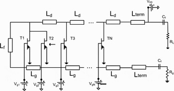
A DVCO can be obtained by introducing a feedback loop in a distributed amplifier. This is achieved by removing the usual drain termination in a distributed amplifier and connecting together the drain and the gate lines by means of a feedback path (Fig. 1). Some of these DVCO architectures [Reference Skvor, Saundres and Aitchitson1–Reference Barros and Correra4] can achieve a wideband frequency tuning range by modifying the gate biasing of the active devices.
Schematic representation of an N-stage DVCO.

Assuming an N element DVCO, the fundamental concept for a wideband frequency tuning lies on the fact that when individually activating each of the active devices while keeping the rest deactivated, one can obtain a set of discrete frequencies (f 1, …, f N) distributed along a wide frequency band. The limits of this frequency band and the spacing between the discrete frequencies are directly related to the parameters of the gate and drain transmission line sections that connect the different active devices (Fig. 1).
The highest discrete frequency f 1 corresponds to the activation of transistor T1 (Fig. 1), which has the shortest feedback path, whereas the lowest discrete frequency f N corresponds to the activation of transistor TN (Fig. 1), which has the longest feedback path. Between f 1 and f N there is a set of discrete frequencies f 2, …, f N−1 corresponding to the activation of the intermediate transistors T2, …, TN−1. Continuous frequency tuning from f k to f k+1 is achieved by activating the transistors in pairs and varying the gate bias voltages of each pair of transistors (V gk, V gk+1).
Analytical results in [Reference Skvor, Saundres and Aitchitson1, Reference Barros and Correra4], showed the need to introduce a crossed transistor between the first and the second stage (T2 in Fig. 1), to assure the fulfillment of a necessary phase condition in order to have a continuous frequency tuning range between the highest frequency f 1 and the lowest one f N. Additionally, in order to avoid spurious oscillations, the terminal sections L term (Fig. 1) have to be designed to effectively match the gate and drain lines to the output loads [Reference Divina and Skvor2].
III. DVCO OPTIMIZED DESIGN
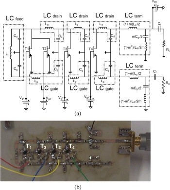
The initial requirements of the designed DVCO are a frequency tuning band from 1 to 2 GHz, minimum consumption, and an output power characteristic with minimum variation along the frequency tuning band. Due to the low-frequency requirements, it is possible to design the DVCO substituting the gate and drain transmission lines (Fig. 1) by their equivalent LC sections (Fig. 2) [Reference Pozar9]. The selected circuit topology has N = 4 stages (Fig. 2) and the active device chosen for this design is the NE3509M04 transistor.
Designed DVCO: (a) schematic representation of the designed four-stage DVCO and (b) implemented prototype of the DVCO.

A) Preliminary design issues of the DVCO
In order to ensure the desired frequency range is covered, the values of L f, L d, C d, L g, and C g in Fig. 2 should be carefully chosen to originate a set of discrete frequencies distributed along the 1–2 GHz frequency band.
The nonlinear design of the DVCO is based on the use of harmonic balance simulation in combination with an auxiliary generator (AG) [Reference Chang, Steer, Martin and Reese6, Reference Georgiadis and Collado7, Reference Suarez, Morales and Quere10]. This AG is introduced into a node of the circuit only for simulation purposes in order to avoid the convergence of the harmonic balance simulator to the trivial solution that always exists in an oscillator circuit. The AG is formed by an ideal generator defined by three variables: amplitude A AG, frequency f AG, and phase ϕ AG. This ideal generator is connected in series with a band pass filter centered at the frequency of the AG. In the steady state the admittance, calculated at the node where the AG is connected to the circuit (Y AG = V AG/I AG), has to be zero in order not to perturb the steady-state solution.
In order to obtain a set of discrete frequencies along the 1–2 GHz frequency band, each of the four transistors is independently biased with a gate bias voltage V g = −0.1 V. Then an AG is introduced into the circuit to calculate the values of the individual discrete frequencies (f 1, f 2, f 3, f 4) versus the values of L d, C d, L g, and C g. For the proposed design, the gate and drain LC sections are chosen to be equal, L d = L g = L, C d = C g = C, and L f = L (Fig. 2).
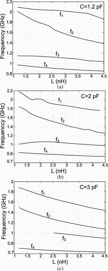
A parametric sweep of L and C is performed and the evolution of the discrete frequencies f 1, f 2, f 3, and f 4 is obtained. For each point of the sweep, the amplitude A AG and frequency f AG of the AG are calculated to fulfill (1) by means of an optimization process [Reference Chang, Steer, Martin and Reese6, Reference Georgiadis and Collado7]. Equation (1) introduces two more equations (Y AGreal = 0, Y AGimag = 0) and two more unknowns (A AG, f AG) in the harmonic balance system of equations:

The family of curves corresponding to the four discrete frequencies f 1, f 2, f 3, and f 4 obtained after the optimization process can be seen in Fig. 3. In Fig. 3(a) the evolution of each of the four discrete frequencies versus L for a fixed value C = 1.2 pF is represented. In Figs 3(b) and 3(c) the same variable is represented for C = 2 and 3 pF. It can be seen that as the value of C increases, the discrete frequencies f 1, …, f 4 corresponding to the activation of T1, …, T4 (Fig. 2) reduce their value which also implies a shifting in the frequency range to lower frequency values. Taking this fact into account in order to cover the desired frequency band from 1 to 2 GHz, a value of the capacitance C = 1.2 pF was selected. The chosen inductance value is L = 3.3 nH as for this inductance value the discrete frequencies f 1, f 2, f 3, and f 4 have a more uniform distribution along the frequency range which ensures a continuous frequency tuning range. The possible spurious oscillations that can appear in the DVCO due to the multiple feedback loops in the circuit are eliminated placing m-derived LC sections (LC term in Fig. 2) immediately before the drain and gate output terminations aiming at matching the gate and drain lines to the output load. In the design, a value of m = 0.6 was chosen to synthesize these terminating sections [Reference Barros and Correra4, Reference Pozar9].
Evolution of the discrete frequencies versus L and C values: (a) C = 1.2 pF, (b) C = 2 pF, and (c) C = 3 pF.

B) Nonlinear analysis of the solution curves of the DVCO
Once the optimum values for the LC sections are chosen, the frequency tuning curves of the DVCO can be obtained using harmonic balance in combination with one AG. The frequency tuning in the designed DVCO is achieved by activating the transistors in pairs. The frequency of the AG, f AG, is swept from 1 –2 GHz and for each point of the sweep the values of the gate bias voltages (V gk, V gk+1) of two consecutive active devices are calculated in order to fulfill Y AG(V gk, V gk+1, A AG, f AG) = 0 by means of an optimization process.
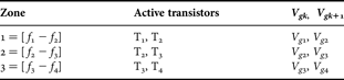
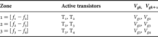
The frequency tuning band is divided into three “zones.” In each of the zones only two transistors are active simultaneously, which implies that only two gate bias voltages are used in the optimization process. The active transistors in each of the frequency zones can be seen in Table 1. The rest of the transistors are deactivated by setting the corresponding gate bias voltages to V g(off) = −1 V. Using the previously mentioned procedure, it is possible to obtain the frequency tuning curves of the DVCO in a continuous manner, by performing only three frequency sweeps.
Active transistors in each of the frequency tuning zones.
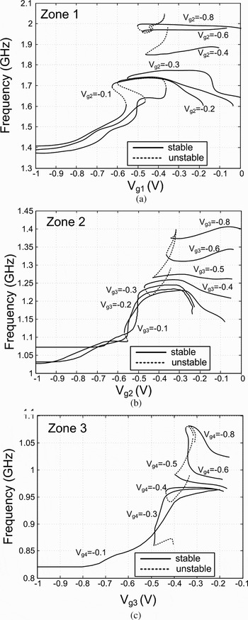
As it can be inferred, a single frequency value can be obtained for different combinations of V gk and V gk+1. This fact can be easily observed by performing a parametric sweep of the two corresponding gate bias voltages V gk and V gk+1 in each of the frequency zones (Fig. 4). The evolution of the frequency in zone 1, zone 2, and zone 3 versus (V g1, V g2), (V g2, V g3), and (V g3, V g4), respectively, is shown in Fig. 4, where it can be seen that some frequency values can be obtained with different combinations of V gk and V gk+1. Furthermore, in Fig. 4 one can identify two types of solution curves in each of the frequency zones. The solutions corresponding to the higher range of frequency values in each zone, which are more closed curves and solutions in the lower part of the frequency ranges which correspond to more open curves. These open solution curves also present larger variations in the output power.
Parametric analysis of the DVCO steady-state solutions versus V gk and V gk+1: (a) frequency versus V g1 and V g2 in zone 1, (b) frequency versus V g2 and V g3 in zone 2, and (c) frequency versus V g3 and V g4 in zone 3.

Another important issue is the fact that the solutions curves in Fig. 4(a) present turning points versus V g1. A turning point or infinite slope point in the solution curves of a system implies a change in the stability of the represented solution. This means some of the solution points in Fig. 4(a) correspond to stable solution points and some of them to unstable solution points. This fact also applies to the solution curves in Figs 4(b) and 4(c). These solutions obtained using harmonic balance require an additional stability analysis in order to determine which of them are stable and consequently observable.
The stability analysis of the solution curves in Fig. 4 is performed using an assisted envelope transient simulation [Reference Ngoya and Larcheveque8]. An AG is connected to the circuit for an initial period of time [0, t0] of the envelope transient simulation. After t0 the AG is disconnected and the circuit is let to evolve to the steady state. The stable sections in the solution curves of Fig. 4 are represented with a continuous line and the unstable sections with a dashed line.
From Fig. 4 the pairs of values (V g1, V g2), (V g2, V g3), and (V g3, V g4) necessary to synthesize each of the frequency values in zone 1, zone 2, and zone 3 respectively, are chosen considering several factors as the output power variation, the maximum output power, and the stability properties of the solution.
C) Optimized frequency tuning and output power characteristics of the DVCO
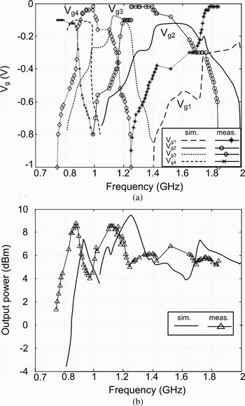
Following the criteria of minimizing the output power variation, the synthesized frequency tuning curves are shown in Fig. 5(a) and the corresponding output power curves in Fig. 5(b). All the represented points correspond to stable points.
Measurements and simulations of the designed DVCO: (a) gate bias voltages versus frequency and (b) output power characteristic versus frequency.

In Fig. 5(b) one can observe the output power variations at the edges of the zones are more abrupt. This phenomenon comes from the fact that in order to get the frequencies solutions that correspond to the lower frequency ranges in each zone, one has to move along the open curves where the output power variation is larger. This variation in the edges of the band is unavoidable if one expects to obtain the maximum frequency tuning range. If minimization of the output power variation is a must, the DVCO should be designed with a larger frequency tuning range in order not to work on the edges of the frequency tuning range and consequently minimize the output power variation.
Superimposed in Fig. 5 one can see the measured results for the designed DVCO. One can see that even though the measurements follow the simulations results close, there is a frequency shift to lower values. Additionally, there are some small gaps in the measured frequency tuning curves, around 0.8, 1.45, and 1.6 GHz where a quasi-periodic spectrum is observed. This is due to a spurious oscillation appearing in the circuit for some values of the gate bias voltages that could be avoided by carefully redesigning the terminating sections LC term (Fig. 2) to improve the gate and drain output matching.
IV. CONCLUSION
Nonlinear simulation techniques based on harmonic balance simulation have been used to design a DVCO. The designed DVCO presents a frequency tuning range from 1 to 2 GHz. The frequency tuning is achieved by controlling the gate bias voltages of two neighbor active devices at a time. A full nonlinear analysis of the different solution curves of the DVCO has been carried out, in order to explain and clarify the behavior of these circuits.
ACKNOWLEDGEMENTS
This work has been supported by the Spanish Ministry of Science and Innovation project TEC2008-02685/TEC, and the PTQ-06-02-0555, PTQ-08-01-06432 grants. This work was also supported by the COST Action IC0803 “RF/Microwave Communication Subsystems for Emerging Wireless Technologies (RFCSET).”
 Ana Collado was born in Santander, Spain. She received the degree in telecommunications engineering and Ph.D. from the University of Cantabria, Santander, Spain, in 2002 and 2007, respectively. In 2002, she worked at the University of the Basque Country, Bilbao, studying the uncertainty in the noise figure measurements in MMIC low-noise amplifiers. Since July 2007 she is working in the Centre Tecnologic de Telecommunications de Catalunya (CTTC) as a research associate in the area of Communications Subsystems. Her areas of interest include the development of techniques for practical bifurcation control, the investigation of coupled-oscillator systems, and stability analysis of power amplifiers.
 Alessandro Acampora was born in Palermo. He received his M.Sc. from University of Palermo, Department of Electrical and Electronics Engineering in 2004. Currently, he is carrying out his Ph.D. studies within the Communication Subsystems area at the=CTTC (Centre Tecnologic de Telecommunications de Catalunya), Barcelona, Spain. His research interests include nonlinear microwave circuit design, focusing on the analysis and design of distributed voltage controlled oscillators to provide wideband tuning capabilities.
 Apostolos Georgiadis (S′94–M′03-SM′08) was born in Thessaloniki, Greece. He received the B.S. degree in physics and the M.S. degree in telecommunications from the Aristotle University of Thessaloniki, Greece, in 1993 and 1996, respectively. He received the Ph.D. degree in electrical engineering from the University of Massachusetts, Amherst, in 2002. In 2002, he joined Global Communications Devices (GCD), North Andover, MA, USA, as a Systems Engineer and worked on CMOS transceivers for wireless network applications. In June 2003, he joined Bermai, Inc., Minnetonka, MN, USA, as an RF/Analog Systems Architect. In 2005, he joined the University of Cantabria, Spain, as a Juan de la Cierva Fellow researcher. In addition, he collaborated with ACORDE S.A., Santander, Spain, in the design of integrated CMOS VCOs for ultra wideband (UWB) applications. In March 2007, he joined CTTC as a senior research associate in the area of Communications Subsystems. In 1996, Dr. Georgiadis received a Fulbright Scholarship for graduate studies at the University of Massachusetts, Amherst. He received the Outstanding Teaching Assistant Award from the University of Massachusetts, Amherst, in 1997 and 1998. He also was the recipient of the Eugene M. Isenberg Award from the Isenberg School of Management, University of Massachusetts, Amherst, in 1999 and 2000. He is the Chairman of COST Action IC0803, RF/Microwave communication subsystems for emerging wireless technologies (RFCSET). He serves as an Associate Editor for the Radioengineering Journal. His research interests include nonlinear microwave circuit design and wireless systems, active antenna arrays, and specifically coupled oscillator arrays.