I. INTRODUCTION
In the last years, there has been a growing demand of wireless devices able to collect and retransmit data by means of a wireless channel. Consequently there was an increasing demand of clean energy sources, able to offer high efficiency, and at the same time to reduce the maintenance operations. Wireless power transmission (WPT) constitutes a method of generating electricity and transport it with electromagnetic (EM) waves [Reference Yagi and Uda1–Reference Sham and Ali6]. Recently several candidate systems have been proposed for different practical applications such as charging ubiquitous electronic devices such as mobile phones and laptops, powering pervasive sensors and actuators (e.g. wireless sensor nodes and robots), and fueling electrical vehicles [Reference Hu7, Reference Kiani8]. The solar power satellite (SPS) is not a new concept, in 1968 P.E. Glaser proposed the idea of solar power station (SPS). The power generated in the space can be beamed down to earth using radio-frequency (RF) signal. He gave a theoretical prediction of around 10 GW of power that can be beamed down by an RF-signal of frequency 5.8 GHz [Reference Brown2]. Recently SPS has gained new interests and innovative techniques have been explored by scientists and engineers all over the world. An SPS constitutes a method for generating electricity from solar energy using satellites and transporting it to the ground via EM waves [Reference McSpadden and Mankins9–Reference Shinohara, Mitani and Matsumoto11]. Due to the increasing cost of petrol, it has been recently considered as an interesting alternative electric power source [Reference Franceschetti, Rocca, Robol and Massa12–Reference Massa, Oliveri, Viani and Rocca14]. Unlike inductive power transfer [Reference Hu7], WPT essentially consists of the RF radiation of the EM power collected far-away from the receiver [Reference Brown2, Reference Spaden, Yoo and Chang3]. In particular, a WPT system can be summarized by means of a three main functional blocks. The first considers a device able to convert direct current (DC) into RF power. The RF power is then transmitted through the space to some distant points, and finally the power is collected and converted back into DC power at the receiving points. The overall efficiency of a WPT system is the product of the individual efficiencies associated with the three main blocks of the system. The goal of WPT designer is the maximization of the power transfer, and to reach this goal the knowledge and the combination of different expertises, such as microwave circuits and devices, antenna design and optimization, and an accurate knowledge of the wireless channel is required. In this framework, this work is aimed at the development of a WPT system able to provide a remote power supply to low-power wireless devices. Low-power electronic devices commonly have a power supply element such as a battery, rechargeable battery, or a capacitor to provide energy for their different electronic circuits and operations. To be recharged, the energy storage unit must be cable-connected to a voltage regulator and to the main power supply network. The standard battery replacement requires expensive maintenance operations. Regulators, wiring, and connectors as well as the energy storage itself, especially in case of a battery, are often a source of errors and extra costs. Moreover, regulators and connectors are not always compatible with different devices, so that each device type needs its own custom-tailored charging solution. The need for wiring, connectors, or even batteries in electronic equipments can be eliminated with WPT. WPT could be an alternative ideal solution in case of a small device, low costs are of fundamental importance or wireless sensors are placed in remote, dangerous, or inaccessible areas. Depending on the application and the employed components, i.e. antennas, rectifiers, and capacitors, different frequencies can be used for power transfer, higher frequency bands allow us to obtain very compact devices. Toward this end, in this paper an optimal WPT system based on a compact planar receiving rectennas array [Reference Rocca, Oliveri and Massa15, Reference Shinohara16] is presented and experimentally assessed. In particular, the optimal receiving array configuration is obtained with suitable antenna optimization techniques, and the theoretical limits for the power transmission efficiency of the WPT system are investigated. The contributions of this work are the use of a one-dimensional (1D) parabolic reflector antenna, which is more compact simple and less subjected to mechanical stress with respect to standard 2D parabolic reflector, moreover it is particularly suitable (thanks to its mechanical robustness) to work in complex and dangerous scenarios (such as earthquakes, avalanches, floods, and landslides). The other contribution is the development of a very compact receiving rectenna array, with a very limited inter-element separation with respect to standard arrays. For the authors knowledge in scientific literature there are no WPT systems based on array of microstrip patch antennas with the same level of compactness. The paper is organized as follows. Section II reports the mathematical formulation and in particular the guidelines for the maximization of the performances of a WPT system. Section III is devoted to the description of the WPT system. Section IV reports the preliminary experimental results performed on a WPT system prototype. Finally in Section V, the conclusions are drawn and areas of future work are examined.
II. MATHEMATICAL FORMULATION
Let us consider the WPT scenario reported in Fig. 1, where a transmitter section transmits a high-power EM wave toward a receiving device placed at distance r and devoted to convert the power associated with the EM wave into (DC) power to supply low-power electronic devices. The transmitting section is composed by a signal generator at microwave frequency bands, a power amplifier, and a high-gain antenna. The receiving section is composed by a rectenna, whose main components are a receiving antenna, a matching network, a harmonic filter, a rectifying unit, and a low-pass filter. Under the assumptions of far-field and line of sight conditions, the power at the output of the receiving section can be easily estimated considering the following relation:
 $${P_{rx}} = \displaystyle{{{P_{tx}}{G_{tx}}{G_{rx}}} \over {{{(4\pi r/{\lambda _0})}^2}}} \cdot {L_{tx}} \cdot {L_{rx}} \cdot {\left \vert {{a_t} \times {a_r}} \right \vert ^2} \cdot {e^{ - \alpha r}}$$
where P tx is the power of the transmitter, provided by the generator and the RF amplifier, G tx is the gain of the transmitting antenna, λ 0 is the free-space wavelength at the fundamental frequency,  ${G_{rx}} = 4\pi {A_e}\lambda _0^2 $ is the gain of the receiving antenna, A e is the so-called effective area and it corresponds to the receiver antenna surface area exposed to the incident microwave energy. The term (4πr/λ 0)2 is the free-space attenuation factor, L tx = 1 − |Γtx|2 and L rx = 1 − |Γtx|2 are the losses due to mismatches in the transmitting and receiving section, respectively, Γ tx and Γ rx are the reflection coefficients measured at the output/input ports of the receiving and transmitting antenna and they can be kept near the theoretical limit, thanks to a proper antenna design and tune. α is the absorption coefficient of the propagating medium, assuming the air as propagation media α can be reasonably considered equal to zero. a t and a r are the polarization vectors of the transmitting and receiving antennas, respectively. Equation (1) is commonly used in telecommunication engineering [Reference Roddy17] and it permits to calculate the power received by a receiving antenna given a transmitting antenna placed at a given distance r from the receiving system and able to transmit a known amount of power P tx. Relation 1 provides information related to the power received at the output port of the receiving antenna, but it is not able to provide information concerning the efficiency of the rectifying unit connected after the receiving antenna. The conversion efficiency of the rectifying unit is provided by the following relation [Reference Spaden, Fan and Chang4, Reference Ren and Chang5, Reference Yoo and Chang18, Reference Ren, Farooqui and Chang19]:
 $${\eta _r} = \displaystyle{{{W_{DC}}} \over {{P_{rx}}}} = \displaystyle{{V_d^2 \cdot {Z_{load}}/({Z_d} + {Z_{load}})} \over {{P_{tx}}{G_{tx}}{G_{rx}}{{({\lambda _0}/4\pi {r^2})}^2} \cdot {L_{tx}} \cdot {L_{rx}} \cdot {{\left \vert {{a_t} \times {a_r}} \right \vert} ^2} \cdot {e^{ - \alpha r}}}}$$
where W DC is the DC power at the output of the rectenna and delivered to the user. P rx represents the incident power on the rectenna circuit, estimated with the Friis formula 1, Z load is the load impedance, V d and Z d are the voltage and the impedance of the rectifying diode, respectively. As it can be noticed from relation 2, the maximum transferred power which maximizes the conversion efficiency is reached by choosing Z d = Z load [Reference Ren and Chang5]. The diode impedance Z d can be estimated by means of the following relations [Reference Ren and Chang5, Reference Akkermans, Van Beurden, Doodeman and Visser20] and the circuital model reported in Fig. 2:
 $${Z_d} = \displaystyle{{\pi {R_s}} \over {{\rm cos}({\theta _{on}})({\theta _{on}}/{\rm cos}({\theta _{on}}) - {\rm sin}({\theta _{on}}))} + {j\omega {R_s}{C_j}((\pi - {\theta _{on}}/{\rm cos}({\theta _{on}})) + {\rm sin}({\theta _{on}}))}}$$
where R s is the junction resistance, C j is the diode capacitance, and θ on is the forwarded-bias turn-on angle which can be numerically estimated by solving the following transcendent equation [Reference Akkermans, Van Beurden, Doodeman and Visser20]:
 $${\rm tan}\left( {{\theta _{on}}} \right) - {\theta _{on}} = \displaystyle{{\pi {R_s}} \over {{Z_{load}}(1 + {V_{bi}}/{V_d})}}$$
where V bi is the forward voltage between the diode junction. It is worth noticed that the parameters R s, Cj, and V bi can be easily derived from the diode data sheet. To maximize the power transfer between the receiving antenna and the user load, good matching conditions between the different sections of the rectenna must be guarantee.
WPT system architecture.

Circuital model of a single rectenna unit.
III. SYSTEM DESIGN
In the following, the description of the S-band WPT system, operating at 3.4 GHz will be detailed. The sections that follow describe the steps for the design of the transmitter and of the receiver rectenna sections.
A) Transmitting section
The transmitting section is composed by a dielectric resonator oscillator (DRO) characterized by P tx = 20 mW and a working frequency of f w = 3.4 GHz, a 4 W GasAsFet power amplifier, and a prime focus parabolic mono-dimensional reflector antenna with a gain of about G tx = 25.1 dB. The DRO and the amplifier are commercial devices from Kunne Electronic Company. Let us focus on the design of the mono-dimensional parabolic transmitting antenna. The mirror design starts from the classical parabola equation y = ax 2 + bx + c the coordinates of the parabola vertex and focus are (−b/2a;−Δ/4a) and (−b/2a; 1 − Δ/4a), respectively, being Δ = b 2 − 4ac. The distance of the focus from the parabola vertex must be kept k(λ/4), k is a positive integer, to guarantee a constructive sum between the signal generated by the feeder and those reflected by the metallic mirror. For the considered WPT system a = 3.75, c = 0 and k = 3 have been considered. At the end of the design procedure a mono-dimensional parabolic metallic mirror with a vertex position and focus coordinates v p = (0;0) and f p = (0;kλ/4) = (0;0.066 m), height a h = 16λ = 0.141 m and width a w = 4λ = 0.353 m. The parabolic mirror has been simulated with a commercial EM full-wave simulator (Ansys HFSS) which confirmed the antenna gain of about G tx ≃ 23 dB. The feeder is a linear array of four half-wavelength (length l = 0.044 m) dipole antennas placed along the focus line of the mono-dimensional parabolic mirror. Each dipole is tuned at the working frequency of f w = 3.4 GHz and equipped with a Sleeve/bazooka balun [Reference Pozar21] to guarantee good match properties. Figure 3 reports the photographs of the four dipoles array placed in the focus of the parabolic mirror, as it can be observed from Fig. 3 the Sleeve/bazooka baluns are composed by quarter wavelength copper pipes directly soldered on the outer conductor of each semi-rigid coaxial cable connected with the dipole antenna. The semi-rigid coaxial cables guarantee the correct position of each dipole in the mirror focus, placed at f = 0.068λ from the mirror vertex. The oscillator and the amplifier are connected with the transmitting antenna by means of a feeding network composed by three 3 dB Wilkinson commercial power splitter, connected together by means of semi-rigid three shielded coaxial cables equipped with sub-miniature type a (SMA) coaxial connectors. The considered feeding network assures the same amplitude and phase for each dipole which correspond to a broadside beam pattern configuration [Reference Balanis22]. Figure 4 shows a photograph of the considered feeding network. The reflection coefficient at the input port of the transmitting antenna was measured with a network analyzer and kept to Γ tx = 0.316 by means of a suitable tuning. The value of the obtained Γ tx is able to guarantee a transmission efficiency (related to the mismatch) of about 1 − |Γ|2 = 0.9. All the microwave components of the transmitting section have been assembled together using a wood pedestal, the results is a compact and light structure. The antenna gain has been measured in a semi-anechoic chamber and a value of about G tx = 24.5 dB has been obtained. The considered semi-anechoic chambers (kindly provided by the EMC Company) have a solid floor that acts as a work surface for supporting heavy items and it's particularly suitable for EM compatibility measurements. To perform antenna measurements such as gain and beam pattern measurements absorbent cones were placed on the floor to obtain a full anechoic chamber. The power supply is provided by means of a rechargeable lead battery. The photograph of the transmitting section prototype is reported in Fig. 5.
Transmitting section. Details of the four dipoles array feeder.
Transmitting section. Details of the combiner, power amplifier (4 W), and DRO oscillator.
Transmitting section. Photograph of the prime focus reflector antenna.
B) Receiving section
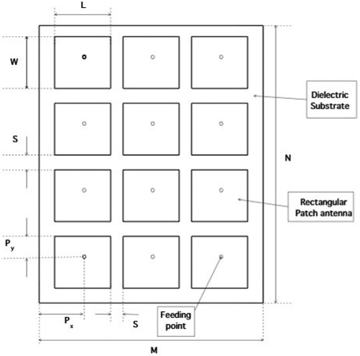
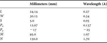
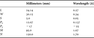
Let us first consider the design of a single rectenna element considering the circuital model reported in Fig. 2. Each rectenna is composed by a rectangular antenna patch, with a coaxial feeding point. If the feeding point is placed at a suitable position from the boundary of the patch, the antenna impedance can be easily tuned and the matching network reported in Fig. 2 can be avoided and the antenna can directly connected to the input port of the harmonic filter with a minimum mismatch [Reference Gupta and Barthia23–Reference Bahl and Bhartia25]. The harmonic low-pass filter inserted between the receiving antenna and the rectifying section is designed, so that the fundamental frequency at f w = 3.4 GHz can be passed and the resultant significant portion of the high harmonics generated from the rectifying unit are reflected back and used. The rectifying unit consists of a diode connected in series with a tank capacitor. The basic principle of the power conversion is analogous to a clamping diode circuit. The power conversion efficiency is maximized when all the high-order harmonics are confined between the low-pass filter and the rectifying diode, this goal can be obtained not only using an high-efficiency diode, but also by providing a good matching between the antenna, the low-pass filter, the diode, and the tank capacitor connected with the user load. It is worth noticing that a single rectenna unit is not able to produce enough power to feed a low-power electronic device such as a wireless sensor network node (WSN). To obtain enough DC power different rectenna units are connected together in a compact array. In particular, an array of 4 × 3 rectenna units was considered, the geometry of the compact rectangular patch antennas array is reported in Fig. 6, the goal is to obtain 12£ rectangular patch antennas, harmonic filter, and rectifying unit with similar performances. To obtain the array geometrical parameters listed in Fig. 6, the design methodologies reported in [Reference Balanis22–Reference Bahl and Bhartia25] have been considered, moreover to better tune the array performances and limiting the coupling effects minimizing the dimension of the array, a tuning phase based on unsupervised techniques have been considered [Reference Azaro, Donelli, Franceschini, Zeni and Massa26, Reference Donelli, Azaro, Massa and Raffetto27]. In particular, the patch antenna dimensions W and L, the position of the coaxial feeding point P x and P y and the distance between two consecutive antenna elements S are certainly critical issue because these design parameters greatly affect the performances of the patch antenna elements (i.e. the voltage standing wave ratio (VSWR) and the mutual coupling). For such a reason, the mechanical dimensions of the patch antennas, the positions of the coaxial feeding points and the distance S necessary to obtain a maximum value of the VSWR less than 2 and a mutual coupling less than –10 dB have been found with a synthesis procedure by means of a particle swarm optimizer (PSO). A suitable cost function proportional to the difference between the electrical performances of the trial structures and the requirements has been minimized. PSO is a stochastic multiple-agent optimization algorithm extensively applied in the framework of applied EM and antenna design and optimization (see [Reference Fimognari, Donelli, Massa and Azaro28–Reference Massa, Franceschini, Franceschini, Pastorino, Raffetto and Donelli35] and references therein) that demonstrated excellent properties of convergences during the optimization process. At the end of the design phase the geometrical parameters summarized in Table 1 have been obtained. The obtained patch array has been first simulated with a commercial EM simulator, namely HFSS designer, to numerically assess the VSWR of each patch antenna parameters, and then for the sake of the assessment each patch antenna has been measured with the network analyzer. The EM simulator indicated a VSWR ≦ 1.353 for all the array elements. At the end of the design procedure the mechanical dimensions of the antenna array are 10 × 15 cm2, while the mechanical dimensions of the wireless sensor node are 4 × 10 cm2. The mechanical dimensions of the antenna array and of the wireless sensor node are perfectly compatible. The design of the low-pass filter is quite trivial, it can be designed following the well-known insertion loss method [Reference Pozar21, Reference Collin36], in particular for the considered WPT system a third-order low-pass Chebyshev filter [Reference Pozar21, Reference Collin36] with a cut-off frequency of f c = 4 GHz has been considered. The impedance of the filter ports was chosen equal to the antenna impedance Z in = Z out = 50 Ω. The filter input port is connected with the antenna and the output port with the rectifying PIN diode. In particular, the filter is composed by two capacitors C 1 = C 2 = 1.27 pF and one inductor L 1 = 2.18 nH organized in a π network [Reference Pozar21, Reference Collin36–Reference Yang, Xu, Xu and Xu39]. The rectenna circuit is completed with a tank electrolitic capacitor C Tank = 42 µF directly connected in shunt with the resistive load. The complete schema of the rectifying unit is reported in Fig. 2, while a photograph of the obtained rectifying circuits connected to the antenna elements can be seen on the left side of Fig. 7.
Receiving section. Schema of the rectennas array.
Receiving section. Photograph of the rectennas array prototype.
Geometrical parameters of the 4 × 3 rectangular patches array.
IV. WPT SYSTEM EXPERIMENTAL ASSESSMENT
Following the design methodologies reported in the previous section, a rectennas array prototype has been designed and built. The 12 patch antennas have been fabricated using a photolithographic printing circuit technology considering the geometrical parameters reported in Table 1. The antennas are printed on one side of t = 0.8 mm ARLON-25N dielectric substrate (ɛ r = 3.28 and Cu metal thickness t m = 10 µm). The photograph of the obtained antennas can be observed on the right side of Fig. 7. The obtained rectennas array was connected with a commercial wireless sensor module, namely the 3MATE! wireless sensor module from the 3TEC Company. The 3MATE! is a very low-power sensor module, particularly suitable for WSNs. The 3MATE! is composed by a microcontroller (the MSP430F161 by Texas Instruments), a radio transceiver, and some environmental sensors (temperature, humidity, and light). Moreover, the above wireless sensor module provides storage capabilities and a set of useful expanding connectors for communication and analog interfacing and it has been specifically developed for low-power consumption. In particular, the maximum power consumption of the transceiver module is 0 dBm (1 mW). Each patch antenna has been equipped with a coaxial feeding point, and experimentally assessed with a network analyzer inside a semi-anechoic chamber. In Figs 8 and 9, the real and imaginary parts of the measured input impedance of all the rectangular patch antennas of the array, as function of frequency are shown. As it can be seen from Fig. 8, at the central frequency of f w = 3.4 GHz the real part of the antennas impedance is near 50 Ω in particular the maximum and minimum values of the real part of the antennas impedances are comprised in the range between 53 Ω<Z a <59 Ω. Since measurement results are in very good agreement with the numerical simulations obtained with the full-wave calculation results, the numerical results are not shown in the figures. The imaginary part of all antennas impedances (at the central frequency of f w = 3.4 GHz) is slightly inductive, and near to +j10 Ω as it can be observed from the results reported in Fig. 9. The realization of the third-order low-pass filter has been obtained considering commercial surface mount devices (SMD) in particular two capacitors C 1 = C 2 = 1.2 pF and one inductor L 1 = 2.18 nH have been used. The diode is an Infineon Technologies BAR64-02V PIN-type diode. The BAR64-02V characteristics taken from the component's data sheet are; diode capacitance C T = 0.0718 pF, reverse parallel resistance R p = 4 KΩ, junction direct resistance R p = 0.5 Ω, and parasitic package inductance L s = 0.6 nH. It is worth noticed that different PIN and low barrier hot-carrier diode models have been experimentally tested as rectifier in the considered WPT system. The BAR64-02V offered the best performances with respect to the other models. Figures 10 and 11 show the real and imaginary parts of the simulated and measured fundamental diode impedance versus frequency for a 0 dBm input power level. The measurements performed with a network analyzer have been done considering only the fundamental frequency; the superior harmonics have been neglected. The noise visible in the measured data (blue line) are due to the fact that the network analyzer is not able to fully suppress the higher harmonics on its input port. Nevertheless the agreement between simulations and measurement is quite satisfactory and prove that the diode circuital model is sufficiently accurate for design purposes. It is worth noticed that the observed ripple is quite high especially for frequency values below 0.5 GHz, this behavior is quite anomalous and it is probably due not only to the higher harmonics contributes, but also to the measurement instrument noise. From the data reported in Figs 10 and 11 at the central frequency of f w = 3.4 GHz the PIN diode shows an impedance of Z d = 53 − j81 Ω. Figure 12 shows the measured rectennas conversion efficiency versus frequency. Since the devices performances change electrically with the frequency, a calibration has been done by measuring the input power for each frequency. As expected changing the frequency influences the rectenna's performances because the antenna impedance is changed. As seen from the data of Fig. 12, a maximum conversion efficiency of 63% occurs at 3.4 GHz. However, the efficiency of all the rectenna units remains above the 52% over a frequency band located between 3.35 and 3.45 GHz. As stated above, a single rectenna unit is not enough to provide the energy necessary to feed a low-power electronic device. The wireless sensor used to test the system requires a minimum DC power of about 10 mW, a DC voltage of about 5 V, and a DC current of about 2 mA. To increase the output voltage the rectennas placed along the rows of the array were connected in series and the row placed in shunt each other to increase the DC output current, in particular three set of four rectenna elements are connected in series to reach a voltage of about 4.5 V mandatory to supply the power stage of the wireless sensor node, the three 4.5 V elements are then connected in shunt to increase the current. With reference to equation (1), with α = 0 since we can assume the vacuum as propagating media, no losses due to polarization |a t × a r|2 = 1 thanks to a suitable antennas alignment, P tx = 4.02 W, G tx = 25, and G rx = 6 dB, a power of about 10 mW can be theoretically obtained at a distance r = 0.8 m. The obtained power is enough to uninterruptly supply the wireless sensor node. The obtained WPT system has been firstly arranged inside a semi anechoic chamber kindly provided by the EMC Company, which offers different professional calibration and measurement services. For the sake of completeness a measurement campaign has been performed also considering different realistic scenarios such as unshielded crowed rooms and corridors. The mismatch between the data collected in the semi-anechoic chamber and the standard locations is less than 10%. The 12-patches antenna array demonstrated to be able to supply the wireless sensor at a distance r = 0.8 m as predicted by relation 1. The maximum power efficiency transfer was 60%, the output voltage 4.8 V, and the DC current about 1.8 mA. For the sake of completeness Fig. 13 reports the theoretical and measured power received by the rectennas array versus distance. The power transfer efficiency η p(f w) (for each element of the rectenna array) can be calculated considering the following relation:
 $$\eta \left( {{f_w}} \right) = \displaystyle{{\left \vert {{I_L}({f_w}){Z_L}} \right \vert} \over {\left \vert {{V_i}({f_w}){I_i}({f_w})} \right \vert \cos (\angle {I_i}({f_w}) - \angle {V_i}({f_w}))}}$$
where I L and Z L are the current across the load and the load impedance, respectively. I i and V i are the current and the input voltage provided by the power supply at the transmitting section. It is worth noticed that the best WPT systems reach a power transfer efficiency between  $50\% \le {\eta _p}({f_w}) \le 70\%.$ The data reported in Fig. 13 have been obtained in the semi-anechoic chamber considering the maximum power available with P tx = 4.02 W, G tx = 25, and G rx = 6 dBi, as confirmed by theoretical as well as experimental measurements a power of about 10 mW is available on the antenna at a distance r = 0.8 m. In particular, the exact measured power at the antenna output was in the following range 8.4 mW<P rx <12.3 mW.
Real part of the measured input impedances of the 12 coaxial fed rectangular microstrip antenna patches.
Imaginary part of the measured input impedances of the 12 coaxial fed rectangular microstrip antenna patches.
Real part of the simulated (red line) and measured (blue line) input impedance of a BAR64-02V PIN diode.
Imaginary part of the simulated (red line) and measured (blue line) input impedance of a BAR64-02V PIN diode.
Measured conversion efficiency of the 12 rectenna circuits.
Rectenna array received power. Comparisons between the estimated and measured power at different distances.
As it can be noticed considering a system efficiency of about 60% the theoretical data are in good agreement with the measures.
V. CONCLUSION
In this work, an S-band system for WPT has been designed fabricated and tested. The WPT system prototype is composed by a transmitting section based on a prime focus mono-dimensional parabolic reflector antenna with a linear feeder composed by an array of four dipoles. The receiving section is made with a compact 3 × 4 rectennas section. Each rectenna element used a rectangular patch antenna, an S-band mixer diode, a third-order harmonic filter and a tank capacitor, the patches antennas are organized in a compact array. Unsupervised methodologies based on evolutionary techniques were used to optimize the transmitting as well as the receiving section and consequently to maximize the power conversion efficiency of the whole system. The experimental assessment demonstrated the effectiveness and the potentialities of the proposed system to supply low-power electronic devices such as wireless sensors and other low-power devices. Future works will be devoted to further improve the miniaturization of the receiving array, and to the improvement of the performances of the rectifying circuit using dielectric resonators.
M. Donelli received his M.Sc. degree in Electronic Engineering and Ph.D. degree in Space Science and Engineering from the University of Genoa, Genoa, Italy, in 1998 and 2003, respectively. He is currently an Associate Professor of electromagnetic field at the Department of Information and Communication Technology, University of Trento, Trento, Italy, and a member of the ELEDIA Research Center. He is the author/coauthor of over 160 peer-reviewed papers in international journals and conferences. His current research interests include microwave devices and systems design, EM inverse scattering, adaptive antenna synthesis, optimization techniques for microwave imaging, wave propagation in superconducting materials, and urban environments.
P. Rocca received the M.S. degree (summa cum laude) in Telecommunications Engineering and the Ph.D. degree in Information and Communication Technology from the University of Trento, Trento, Italy, in 2005 and 2008, respectively. His main interests are in the framework of antenna array synthesis and design, electromagnetic inverse scattering, and optimization techniques for electromagnetics. He is currently an Assistant Professor at the Department of Information Engineering and Computer Science, University of Trento and a member of the ELEDIA Research Center. He is the author/coauthor of over 160 peer-reviewed papers in international journals and conferences. He has been a visiting student at the Pennsylvania State University, Philadelphia, PA, USA and at the University Mediterranea of Reggio Calabria, Reggio, Calabria, Italy. Dr. Rocca has been awarded the best Ph.D. dissertation award by the IEEE Geoscience and Remote Sensing Society and the Italy Section (IEEEGRS Central Italy Chapter). He serves as an Associate Editor of the IEEE ANTENNAS AND WIRELESS PROPAGATION LETTERS.
F. Viani received the M.S. degree in Telecommunication Engineering from the University of Trento, Trento, Italy, in 2007 and the Ph.D. degree in Information and Communication Technology from the International Doctorate School, University of Trento, Trento, Italy, in 2010. He is currently a member of the ELEDIA Research Center at the Department of Information Engineering and Computer Science (DISI), University of Trento. His main interests are in wireless sensor networks, antenna synthesis and design, industrial application of wireless power transmission technologies, and electromagnetic inverse scattering methodologies.