Conjugated polymers are a widely studied class of semicrystalline organic semiconductors, exhibiting very different morphologies and physical properties, depending on their method of fabrication. Typically, thin polymer films are deposited from solution, which is the simplest strategy and most amenable for high-throughput, and low-cost fabrication. However, there are a number of situations wherein vacuum-based deposition provides advantages, such as creating patterned or multi-layered architectures, or in cases where the desired substrate or surface has poor wettability.[ Reference Wu, Ringeisen, Callahan, Brooks, Bubb, Wu, Piqué, Spargo, McGill and Chrisey 1 , Reference Caricato and Luches 2 ] Conventional physical vapor deposition techniques are unsuitable, as they involve large energy input which generally degrades polymeric materials. In recent years, however, an increasing number of groups have successfully fabricated polymer films using an analog of pulsed laser deposition known as matrix-assisted pulsed-laser evaporation (MAPLE).[ Reference McGill, Chrisey, Pique and Mlsna 3 – Reference Chrisey, Piqué, McGill, Horwitz, Ringeisen, Bubb and Wu 5 ] Rather than directly ablating solid polymer, the MAPLE process utilizes a frozen dilute solution of the polymer and volatile solvent. Under ideal circumstances, laser energy is almost entirely absorbed by the host solvent “matrix”, thereby preventing photochemical degradation of the guest polymer.
The MAPLE technique affords access to films with unique morphologies, associated with physical properties/phenomena, such as density and glass transition temperature, that differ from that of normal solvent cast films.[ Reference Guo, Morozov, Schneider, Chung, Zhang, Waldmann, Yao, Fytas, Arnold and Priestley 6 , Reference Shepard, Guo, Arnold and Priestley 7 ] While interesting and promising findings have been reported for MAPLE-deposited conjugated polymers and nanocomposites for solar cells and other optoelectronic devices,[ Reference Gutiérrez-Llorente, Horowitz, Pérez-Casero, Perrière, Fave, Yassar and Sant 8 – Reference Ge, Atewologun and Stiff-Roberts 11 ] the fundamental relationships between morphology and electronic properties in such films remain poorly understood. Herein, we investigate the carrier transport characteristics of MAPLE-deposited poly(3-hexylthiophene) (P3HT) films, both in- and out-of-planes, connecting the unusual behaviors with the unique morphologies. Whereas the in-plane carrier mobilities of MAPLE-deposited films are comparable with those of spin-cast analogs, the out-of-plane mobilities are an order of magnitude lower. The out-of-plane carrier transport is rationalized in terms of the well-established Gaussian Disorder Model (GDM), which describes carriers traversing through an environment characterized by both positional disorder, associated with the morphology, and energetic disorder (broadening of the density of states, originating from a distribution of conjugation lengths). Our results provide new insights into the role of structural and energetic disorder on the in- and out-of-plane carrier transport in conjugated polymer thin films.
Since the early development of the technique, the majority of MAPLE systems employed excimer lasers emitting ultraviolet (UV) wavelengths. Later it has been shown that UV lasers could degrade the dilute polymer guest; even when the chemical functionality was preserved, a reduction in molecular weight (due to chain fragmentation) was often observed in the deposited material. Photochemical degradation is of particular concern for conjugated polymers, whose absorption extends all the way into the visible spectrum. To circumvent this problem, we employed resonant infrared (RIR-MAPLE).[ Reference Greer 12 ] Our MAPLE system (PVD Products) is equipped with an Er:YAG laser (Quantel) that produces a wavelength of 2.94 µm, well beyond the absorption edge of conjugated polymers and resonant with the vibrational stretching mode of hydroxyl bonds, making water the ideal solvent matrix. Since most conjugated polymers are not water-soluble, including the P3HT used in this study (Rieke Metals, mol. wt. 50–70 kDa), we adopted an emulsion-based approach pioneered by the Stiff-Roberts's group.[ Reference Pate, Lantz and Stiff-Roberts 9 , Reference Ge, McCormick, Nyikayaramba and Stiff-Roberts 13 ] In this strategy, the polymer is first dissolved in a good organic solvent (5 mg/ml P3HT in 1,2-dichlorobenzene), then mixed with benzyl alcohol and deionized (DI) water (containing 0.005 wt.% sodium dodecyl sulfate surfactant) at a 1:0.3:3 ratio, and then shaken and ultrasonicated to generate a homogeneous emulsion. The emulsion is injected into a pre-cooled target cup (ca. −170 °C), and once it has been fully frozen, the chamber is pumped to high vacuum (<2 × 10⁻⁵ torr). During deposition, the target is kept at a constant rotation, while the laser (fluence of ~1.3 J/cm2 at the repetition rate of 5 Hz) is rastered across the surface for uniform ablation. The substrates are suspended face-down 5.5 cm above the target, and are also kept at a constant rotation to maintain uniform deposition.
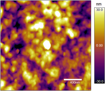
Atomic force microscopy (AFM) was used to characterize the morphologies of the MAPLE-deposited films. As shown in Fig. 1, the surface of the film is quite rough and consists of globular features a distribution of sizes (diameters ranging from 50 to 200 nm). This type of inhomogeneous globular morphology is consistent with those reported in previous MAPLE studies, arising from the mechanisms of target ablation and material transport to the substrate.[ Reference Leveugle and Zhigilei 14 , Reference Shepard, Arnold and Priestley 15 ] Films cast on the silicon (Si) substrates were floated by etching away the native oxide layer, via immersion in dilute hydrofluoric acid, and picked up onto new substrates with the formerly buried interface now exposed at the surface. AFM scans of these flipped films showed very similar globular features on the underside, suggesting that this type of morphology persists across the entire thickness of the film, again consistent with previously reported work.[ Reference Shepard, Guo, Arnold and Priestley 7 , Reference Shepard, Arnold and Priestley 16 ]
AFM topography (2 × 2 µm) of a MAPLE-deposited P3HT film.

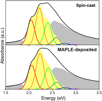
The optical properties of spin-cast and MAPLE-deposited films (both with average thicknesses of ca. 55 nm), were measured using UV–visible (UV–vis) absorbance spectroscopy. In spite of the very different morphologies, compared with spin-cast films, the absorption spectrum of the MAPLE-deposited films are qualitatively similar, as shown in Fig. 2. The total absorption can be deconvoluted into individual peaks by applying the Spano model, from which the exciton bandwidth W and Gaussian disorder parameter σ can be calculated (details of the Spano fitting may be found in the Supplementary Materials).[ Reference Spano 17 , Reference Spano 18 ] Interestingly, although the σ value for the MAPLE-deposited film is larger than the spin-cast counterpart (82 versus 76 meV), the exciton bandwidths W are almost identical (107 meV) and comparable with values reported in literature for P3HT spin-cast from high boiling point solvents.[ Reference Spano 17 , Reference Clark, Chang, Spano, Friend and Silva 19 ] In the limit of weak excitonic coupling between cofacially-packed P3HT chains, the interchain coupling leads to the formation of vibronic bands characterized by an exciton bandwidth W. An increase in the conjugation length leads to greater exciton delocalization across polymer chains and reduces W.[ Reference Gierschner, Huang, Averbeke, Cornil, Friend and Beljonne 20 , Reference Spano and Silva 21 ] The closely matched values of W therefore suggest the similar conjugation lengths, on average, between the spin-cast and MAPLE-deposited samples. The larger magnitude of the disorder parameter σ, however, indicates a wider distribution of conjugation lengths, which most likely stems from a higher degree structural disorder and inhomogeneity (as suggested from the distribution of globule sizes) in the MAPLE-deposited sample.
UV–vis absorption spectra for spin-cast and MAPLE-deposited P3HT films. The total absorption is shown by the black curve, and the yellow and gray-shaded regions represent contributions from aggregate and amorphous fractions, respectively. Aggregate absorption is further decomposed into individual peaks (colored curves) fitted to the Spano model.

To quantify the in-plane charge transport characteristics of P3HT films, thin film transistors (TFTs) were fabricated in top-contact, bottom-gate configuration on substrates of highly doped Si with 300 nm of thermally grown SiO2 (Encompass Inc.). Prior to polymer deposition, substrates were cleaned by ultrasonication in soap, DI water, acetone, hot Hellmanex solution, isopropanol, and boiling isopropanol for 5 min each, followed by UV-ozone cleaning for 20 min. Self-assembly monolayers of octadecyltrichlorosilane (OTS) (Sigma-Aldrich) were grown on the SiO2 surface by immersing substrates in a mixture of OTS and hexadecane (1:250 by volume) for 14 h while stirring. After depositing of polymer films (ca. 50 nm thick), source and drain gold electrodes (Kurt J. Lesker, 99.99%) were vacuum-deposited on top of the polymer film at a rate of 0.5 A/s, using a shadow mask to generate transistor channel length and width of 50 and 500 µm, respectively. All TFT measurements were performed in an oxygen and moisture-free N2-filled glove box using the Agilent 4156C Parameter analyzer. The hole mobility μ was extracted from the drain current I D by fitting the transfer curve in the saturation regime (V D = −80 V) according to:
 $${I_{\rm D}} = \displaystyle{{W{C_{\rm i}}} \over {2L}}\mu {({V_{\rm g}} - {V_{\rm t}})^2},$$
where W and L are the channel width and length, C i = 10 nF/cm2 is the capacitance per unit area of the insulating SiO2 layer, V g and V t are the gate and threshold voltages.
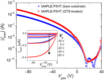
Shown in Fig. 3 are the transfer and output characteristics of TFTs fabricated from MAPLE-deposited P3HT films. Samples deposited on both bare and OTS-treated substrates show transfer curves with a clear onset of current and I on/I off ratio >104. The output current (Fig. 3 inset) also exhibits the typical transistor characteristics, showing a transition from linear to saturation behavior with increasing drain voltage. Transistor parameters for devices with spin-cast and MAPLE-deposited P3HT films are compared in Table I.
Transfer and output (inset) characteristics of transistors made from MAPLE-deposited P3HT on bare and OTS-treated substrates.

Summary of transistor parameters: on/off ratio (I on/I off), hole mobility (μ), threshold voltage (V t) and subthreshold slope (S) for spin-cast and MAPLE-deposited devices, on bare and OTS-treated substrates.

The values reported here were averaged over five different samples.
a Subthreshold slope could not be fitted for devices on bare substrates due to nonlinearity.
As shown in Table I, the in-plane mobilities of MAPLE-deposited P3HT samples are comparable with those of spin-cast counterparts. In TFT measurements, the applied gate voltage draws carriers toward the substrate, and thus in-plane transport is primarily sensitive to the region of elevated carrier density within a few nanometers of the dielectric interface.[ Reference Dinelli, Murgia, Levy, Cavallini, Biscarini and de Leeuw 22 ] For the spin-coated devices, OTS treatment of the SiOx substrate produces nearly an order of magnitude increase in the hole mobility. This improvement is similar to results reported elsewhere, and has been attributed to improved ordering of polymer chains at the buried interface due to favorable interactions between the alkyl side chains and the self-assembled monolayer.[ Reference Salleo, Kline, DeLongchamp and Chabinyc 23 , Reference Joseph Kline, McGehee and Toney 24 ] The MAPLE-deposited devices, on the other hand, show less than a threefold enhancement in mobility following OTS treatment, which suggests that the morphology of MAPLE-deposited films is less sensitive to the chemistry of the surface upon which they are deposited.
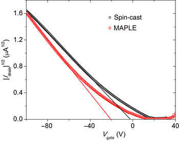
Another notable characteristic of MAPLE-deposited transistors, for both bare and OTS-treated substrates, is the large threshold voltage (V t), calculated from the intercept of the linear regime with the voltage axis, as illustrated in the plot of |I drain|1/2 versus gate voltage in Fig. 4. The subthreshold regime is ubiquitous in OFET transfer curves, and is associated with the presence of carrier traps or tail states within the band gap. In this regime, mobility increases with the magnitude of V g, as the rising carrier density fills trap states allowing more carriers to access delocalized states near the transport level. When V g is sufficient to fill the density of states to the transport level, the mobility becomes constant.[ Reference Sirringhaus 25 ] The larger subthreshold slope S (reciprocal of the slope of |I D|1/2 versus V g) and broader subthreshold regime of the MAPLE-deposited device reflect a more gradual turn-on transition, while trap states are filled. This is consistent with the larger degree of disorder indicated by UV–vis, which would produce a broader density of states and require additional driving force from V g to fill trapped tail states extending deeper into the band gap.
Plots of |I|1/2 versus V gate comparing MAPLE-deposited and spin-cast P3HT transistors (both on OTS-treated substrates). The solid lines represent the linear regimes from which mobilities are calculated.

In spite of the larger subthreshold regime, we would like to emphasize that the linear regime mobilities of MAPLE-deposited P3HT samples are comparable with or higher than their spin-cast counterparts. This apparent decoupling of disorder and carrier mobilities is rather unusual, and may provide fresh insight regarding the extent to which structural disorder impacts charge transport. Indeed, the paradigm for engineering high-mobility polymers has evolved significantly over the past few years; in a recent review, Himmelberger and Salleo suggest that inevitable structural disorder in polymeric semiconductors does not necessarily prohibit efficient transport, and that future design of these materials should focus on “resilience” to disorder rather than trying to suppress it.[ Reference Himmelberger and Salleo 26 ]
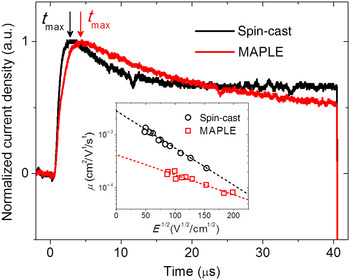
For out-of-plane carrier mobility measurements, the technique of charge extraction by linearly increasing voltage (CELIV) was employed.[ Reference Juška, Arlauskas, Viliūnas and Kočka 27 , Reference Huang, Glynos, Frieberg, Yang and Green 28 ] CELIV holds advantages over traditional techniques such as time of flight or space charged limited current measurements because of its ability to measure mobilities in films of submicron thickness films and films with defects and unintentional doping.[ Reference Blom, de Jong and Vleggaar 29 , Reference Kirchartz 30 ] Triangle voltage ramps were generated by a BK Precision 4075 function generator, and the responded current was then amplified using a FEMTO amplifier before recorded by a Tektronix digital oscilloscope. All CELIV measurements were conducted in a vacuum cryostat (Janis Inc.). Shown in Fig. 5 are representative curves of current density versus time for spin-cast and MAPLE-deposited samples. In a CELIV measurement, there are two major contributions to the responded current: the displacement current j(0) arising from the geometric capacitance of the sample, and the transient drift current Δj = j–j(0) resulting from the extraction and flow of charge carriers within the film. The hole mobility μ is calculated using the drift current Δj, the displacement current j(0), the film thickness h (ca. 100 nm), the ramping rate A and the time t max at which the current reaches a maximum value using the relation[ Reference Juška, Arlauskas, Viliūnas, Genevičius, Österbacka and Stubb 31 ]
 $$\mu = \displaystyle{{2{h^2}} \over {3A{t^2}_{\max} [1 + 0.36(\Delta j/j(0))]}}.$$
Representative current transients measured by CELIV for spin-cast and MAPLE-deposited P3HT films (ramping rate A = 25,000 V/s), and inset showing the electric field dependence of carrier mobilities.

To preface the discussion of out-of-plane carrier mobilities, it is important to recognize that CELIV and TFT measurements probe different regions of the film (bulk versus dielectric interface), which will necessarily lead to different results from in-plane mobilities. It can be immediately observed from the raw CELIV data that the time t
max corresponding to the peak of the transient current is longer for the MAPLE-deposited sample, corresponding to lower out-of-plane carrier mobility according to Eq. (2). The MAPLE sample also exhibits a pronounced broadening of the transient current, indicative of more dispersive transport than the spin-cast sample; this is consistent with higher structural disorder and a larger density of trap states. The electric field dependencies of mobilities (shown in Fig. 5 inset) were determined by changing the voltage ramping rates, A (electric field E = At
max/h). Although the mobilities of the MAPLE-deposited sample are lower than those of the spin-cast sample, they both exhibit linear dependence on E
1/2,
 $\mu = {\mu _{E = 0}}\exp {\kern 1pt} (\beta {E^{1/2}})$
, represented by the dashed lines in the plot. Additionally, the CELIV measurement reveals a weaker electric field dependence of out-of-plane mobility in the MAPLE-deposited sample (β = −3.6 × 10⁻³ cm1/2/V1/2 versus β = −7.0 × 10⁻³ cm1/2/V1/2 for spin-cast).
We can rationalize these trends using the well-established GDM, which describes carriers traversing through an environment characterized by both positional and energetic disorder.[ Reference Bässler 32 ] In a system with a high degree of positional disorder, there exist both fast (high mobility) and slow (low mobility) carrier transport pathways. Due to their structural anisotropy, semicrystalline morphologies, and the presence of both intramolecular and intermolecular transport mechanisms, conjugated polymers are almost always dominated by positional disorder. At low fields, it is more favorable for carriers to travel along fast pathways through strongly coupled transport sites with low energetic barriers, even if it requires following longer, more tortuous routes. Under higher electric fields, however, carriers are increasingly forced to travel along more direct but energetically unfavorable pathways, leading to a lower mobility and hence the negative dependence of the mobility on electric field.[ Reference Huang, Glynos, Frieberg, Yang and Green 28 , Reference Mozer and Sariciftci 33 , Reference Dong, Huang, Tan and Green 34 ]
Energetic disorder, on the other hand, is associated with electrostatic effects and a broadening of the density of states, originating from a distribution of conjugation lengths arising from distortions in the polymer backbone. When energetic disorder is dominant, the applied external field lowers the activation energy for forward hopping of carriers, resulting in a positive dependence of carrier mobility on the electric field. The negative field dependence of mobility in the MAPLE-deposited P3HT sample indicates that positional disorder remains dominant, but the weaker dependence compared with the spin-cast sample may reflect a higher degree of energetic order. This would be consistent from the disorder parameter σ obtained from the Spano analysis of the optical absorption, as well as the higher trap densities suggested by the larger threshold voltages in the TFT output characteristics.
Returning to the out-of-plane carrier mobilities, the zero-field mobility μ E=0 of the MAPLE-deposited sample was extrapolated to be 4.1 × 10⁻⁴ cm2/V/s, nearly an order of magnitude lower than that of the spin-cast sample (2.7 × 10⁻³ cm2/V/s). This is a marked contrast to the comparable or even slightly higher in-plane mobilities measured in TFTs. As previously noted, this apparently divergent trend could be a direct consequence of the differences between the two measurement techniques. Unlike TFT measurements, in which carrier density is greatly enhanced within transport region near the dielectric interface, CELIV extracts intrinsic carriers throughout the bulk of the film. Since the effective carrier densities are much lower in the CELIV measurement of the out-of-plane mobilities, there would be correspondingly higher densities of unfilled trap states that impede carrier transport. Another reason for lower out-of-plane mobilities in the MAPLE-deposited samples could be that the polymer chains adopt orientations predominantly parallel to the substrate. Under this scenario, out-of-plane carrier migration relies more heavily upon interchain transport, which is more sensitive to structural disorder than intrachain transport.[ Reference Noriega, Rivnay, Vandewal, Koch, Stingelin, Smith, Toney and Salleo 35 , Reference Mollinger, Krajina, Noriega, Salleo and Spakowitz 36 ] Given the evidence of more disordered morphologies produced by MAPLE deposition, it follows that the out-of-plane transport in these films would be impacted more significantly than the spin-cast analogs. We attempted to characterize the backbone orientations of MAPLE-deposited P3HT films using spectroscopic ellipsometry, but the high surface roughness complicated data modeling/interpretation.[ Reference Dong, Huang, Tan and Green 34 ] In future experiments, we plan to improve film smoothness and increase the size of the multi-sample analysis of optical constants.
In conclusion, we deposited thin films of P3HT using emulsion-based RIR-MAPLE, and took advantage of the unique resulting morphologies to study the effect of structural disorder, on both in- and out-of-plane charge transports. Optical spectroscopy and carrier transport measurements all show signatures of higher degrees of energetic disorder in MAPLE-deposited films compared with the spin-cast analogs. Interestingly, the increased disorder did not reduce the in-plane transistor mobilities, but had a significant detrimental impact on the out-of-plane mobilities. This striking contrast may, in part, be connected to the unequal sensitivities to disorder of intrachain and interchain transport, which have different relative contributions to the in-plane versus out-of-plane carrier pathways. We also rationalize the different field-dependencies of out-of-plane carrier transport in terms of the GDM, which describes charges traversing through an environment characterized by both positional and energetic disorder. Our findings provide important insight on the effect of disorder on the different mechanisms of charge transport in conjugated polymers.
Supplementary materials
Supplementary material for this article, please visit http://dx.doi.org/10.1557/mrc.2015.72
Acknowledgments
We thank Wangyao Ge (Professor Adrienne Stiff-Roberts's group, Duke University) for helpful advice regarding the emulsion-based RIR-MAPLE technique. Support for this research from the University of Michigan is greatly acknowledged. Equipment purchase was funded as part of the Center for Thermal and Solar Energy Conversion, an Energy Frontiers Research Center supported by the U.S. Department of Energy, Office of Science, Basic Energy Sciences under Award No. DE-SC-0000957.