Plastic solar cells are receiving increasing attention as a renewable energy option due to their flexibility for diverse applications, ability to be printed economically on a mass-scale, and the fast improvements in power conversion efficiency that are being reported by the research community.[ Reference Wienk, Turbiez, Gilot and Janssen 1 , Reference Li, Hendriks, Furlan, Roelofs, Wienk and Janssen 2 ] Currently in the plastic solar cell research field four key focuses include: (a) lowering the material band gap in order to harvest a larger portion of the solar spectrum,[ Reference Zhou, Wei, Yamakawa, Zhang, Tajima, Yang and Hashimoto 3 , Reference Sonar, Singh, Li, Ooi, Ha, Wong, Soh and Dodabalapur 4 ] (b) tuning the blend morphology such that the donor and acceptor material domains are of a similar size as the exciton diffusion length,[ Reference Li, Hendriks, Furlan, Roelofs, Wienk and Janssen 2 , Reference Liu, Gu, Jung, Jo and Russell 5 ] (c) investigating means of printing the photoactive materials from environmentally friendly solvents,[ Reference Holmes, Ulum, Sista, Burke, Wilson, Stefan, Zhou, Dastoor and Belcher 6 , Reference Vaughan, Williams, Holmes, Sonar, Dodabalapur, Dastoor and Belcher 7 ] and (d) improving the stability of the photoactive layer to both photochemical and morphological degradation.[ Reference Lindqvist, Bergqvist, Bäcke, Gustafsson, Wang, Olssen, Inganäs, Andersson and Müller 8 , Reference Guerrero and Garcia-Belmonte 9 ] Here we report a nanoparticle (NP) photoactive layer prepared from the low band gap polymer PDPP-TNT [poly(3,6-dithiophene-2-yl-2,5-di(2-octyldodecyl)-pyrrolo[3,4-c]pyrrole-1,4-dione-alt-naphthalene)] and fullerene acceptor phenyl C71 butyric acid methyl ester (PC71BM) that seeks to address all four of these criteria. That is, PDPP-TNT possesses an optical band gap of 1.5 eV,[ Reference Sonar, Singh, Li, Ooi, Ha, Wong, Soh and Dodabalapur 4 ] NPs have been fabricated from PDPP-TNT (in a blend with PC71BM) that enable films to be spin coated from water-based inks, and the NP films are morphologically stable under thermal stress, with the maximum conditions tested being 130 °C for 60 min and 150 °C for 10 min.
NP photoactive layers represent a new and interesting option for tailoring the donor–acceptor (D–A) domain size at the nanoscale. The semiconductor material domain sizes can be controlled prior to film deposition by altering particle size, as well as post-deposition by applying thermal annealing treatments. While considerable effort is invested by the wider research community into optimizing the nanoscale morphology of interpenetrating donor and acceptor materials in organic photovoltaic (OPV) photoactive layers [whether they be solution-cast bulk heterojunction (BHJ) or nanoparticulate], it is also recognized that stable materials and morphology are required for the long-term operation of the solar cells; especially given that a common degradation process in OPV devices is gross phase separation of pure material domains.[ Reference Bertho, Janssen, Cleij, Conings, Moons, Gadisa, D'Haen, Goovaerts, Lutsen, Manca and Vanderzande 10 , Reference Müller 11 ] A simple method of gauging morphological stability is heating the photoactive layer to 85 °C (the maximum standard OPV operating temperature),[ Reference Reese, Gevorgyan, Jørgensen, Bundgaard, Kurtz, Ginley, Olson, Lloyd, Morvillo, Katz, Elschner, Haillant, Currier, Shrotriya, Hermenau, Riede, Kirov, Trimmel, Rath, Inganäs, Zhang, Andersson, Tvingstedt, Lira-Cantu, Laird, McGuiness, Gowrisankerm, Pannone, Xiao, Hauch, Steim, DeLongchamp, Rösch, Hoppe, Espinosa, Urbina, Yaman-Uzunoglu, Bonekamp, van Breemen, Girotto, Voroshazi and Krebs 12 ] or above, and checking for signs of morphological degradation. The excellent photochemical, mechanical, and thermal stability reported for DPP-based materials makes them a promising option, and has led to their extensive use as high-performance pigments in paints, plastics, and inks.[ Reference Tamayo, Walker and Nguyen 13 ]
Initial reports of the use of DPP-based polymers in NPs for OPV applications have shown encouraging results for this new material system.[ Reference Vaughan, Williams, Holmes, Sonar, Dodabalapur, Dastoor and Belcher 7 , Reference Yamamoto, Payne, Koehler, Facchetti, Roman and Arias 14 ] However, these studies did not investigate the morphology of the NPs beyond that of simple imaging of the film surface. The correct phase separation within the photoactive layer, more specifically the size and purity of the donor and acceptor material domains, is crucial to the successful function of that layer in an OPV device.[ Reference Liu, Gu, Jung, Jo and Russell 5 ] In addition, once the photoactive layer morphology has been optimized, the susceptibility of this morphology to thermal degradation during OPV operation is of paramount importance to the lifetime of solar cells. This paper investigates the morphology of PDPP-TNT:PC71BM NP layers, and the subsequent stability of these layers to morphological degradation.
PDPP-TNT:PC71BM NPs were fabricated with a blend ratio of 1:2 donor:acceptor material using the miniemulsion method reported previously.[ Reference Holmes, Nicolaidis, Feron, Barr, Burke, Al-Mudhaffer, Sista, Kilcoyne, Stefan, Zhou, Dastoor and Belcher 15 ] A summary of this method is provided in Electronic Supplementary Information. A 1:2 donor:acceptor ratio was chosen as it had previously been reported as the optimized ratio for DPP-based polymer:PC71BM BHJ OPVs.[ Reference Wienk, Turbiez, Gilot and Janssen 1 Reference Holmes, Ulum, Sista, Burke, Wilson, Stefan, Zhou, Dastoor and Belcher 6 – Reference Li, Roelofs, Wienk and Janssen 19 ] The NP size and size distribution were measured by applying a circular Hough transform algorithm to scanning electron microscopy (SEM) images of spin coated NP films (Fig. S1) giving a mean particle diameter of 113 ± 42 nm and a median of 106 nm.
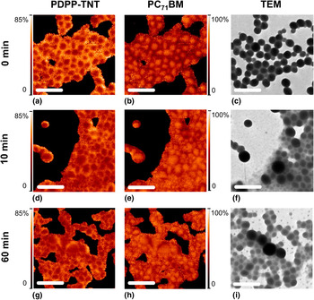
Near-edge X-ray absorption fine structure (NEXAFS) spectroscopy was utilized in order to determine key absorption energies of PDPP-TNT and PC71BM. The NEXAFS spectra of PDPP-TNT and PC71BM are presented in Fig. S2 in Electronic Supplementary Information. An energy of 284.5 eV for PC71BM and both 285.2 and 287.8 eV for PDPP-TNT were chosen for compositional mapping of the PDPP-TNT:PC71BM NP films using scanning transmission X-ray microscopy (STXM). PDPP-TNT:PC71BM 1:2 NPs were spin coated onto silicon nitride (Si3N4) window membrane substrates, and then rastered with respect to the incident beam to produce X-ray absorption images at the three energies. More detail on the STXM and NEXAFS measurements performed at the Advanced Light Source on beamline 5.3.2.2 can be found in the Electronic Supplementary Information. SVD (singular value decomposition) fitting was performed to generate composition maps for PDPP-TNT and PC71BM, these are presented in Figs. 1(a) and 1(b) for as-cast NPs, with matching transmission electron microscopy (TEM) [Fig. 1(c)] performed on a Jeol JEM-1011 TEM. A core–shell NP morphology was observed for all sizes of PDPP-TNT:PC71BM NPs imaged, down to the resolution of the STXM instrument. The STXM compositional maps were used to calculate the PDPP-TNT and PC71BM concentrations in the two NP domain types, with the NP shells being rich in polymer (70–85% PDPP-TNT) and the NP cores rich in fullerene (74–96% PC71BM).
STXM fractional composition maps showing the concentration of PDPP-TNT (left column) and PC71BM (middle column), with matching TEM (right column) in spin-coated 1:2 PDPP-TNT:PC71BM NPs (a–c) as-cast (0 min), (d–f) annealed at 130 °C for 10 min, and (g–i) annealed at 130 °C for 60 min. All scale bars are 600 nm. The color contrast is scaled such that light colors correspond to higher component concentrations. Minima and maxima for the color scale are black = 0 and white = 100%, with the exception of (a), (d), and (g) where white is set to 85% for a clearer visualization of morphology.

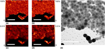
Thermal annealing is a widely used tool for making modifications to the morphology of as-cast organic semiconductor films in a controlled way.[ Reference Müller 11 ] Various thermal annealing treatment conditions were applied to the PDPP-TNT:PC71BM NP films and the resultant morphology was investigated using STXM and TEM. The annealing conditions included 130 °C for 10 min [Figs. 1(d)–1(f)], 130 °C for 60 min [Figs. 1(g)–1(i)] and 150 °C for 10 min (Fig. 2). Each thermal treatment effectively sintered the NPs together (most clearly observed in the matching TEM images shown in Figs. 1 and 2 where NP polymer-rich shells join together), but the overall core–shell intra-particle morphology remained intact; resulting in a morphology beneficial for charge transport through the bulk film to the electrodes.[ Reference Holmes, Nicolaidis, Feron, Barr, Burke, Al-Mudhaffer, Sista, Kilcoyne, Stefan, Zhou, Dastoor and Belcher 15 ]
STXM fractional composition maps showing the concentration of (a) PDPP-TNT and (b) PC71BM, with (c, d) corresponding STXM mass plots and (e) matching TEM for 1:2 PDPP-TNT:PC71BM NPs annealed at 150 °C for 10 min. All scale bars are 1 µm. The color contrast is scaled such that light colors correspond to higher component concentrations. Minima and maxima for the color scale bar in (a) and (b) are black = 0 and white = 100%. For (c) and (d) the color scale bars indicate concentration of component in mg/cm2.

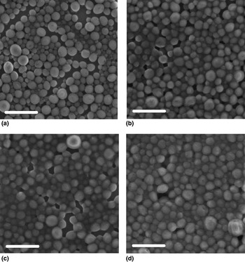
The annealing study was then repeated on additional PDPP-TNT:PC71BM NP films spin cast onto conductive silicon substrates and the morphology investigated via SEM on a Zeiss Sigma ZP FESEM (see Electronic Supplementary Information for more detail on sample preparation). The SEM data presented in Fig. 3 for all three annealing conditions confirms the result obtained from STXM and TEM; the PDPP-TNT:PC71BM NP films are largely stable to annealing at these conditions, with only subtle joining (sintering) of the NPs observed. This result is significant in comparison with other OPV material systems, such as the commonly utilized poly(3-hexylthiophene) (P3HT): phenyl C61 butyric acid methyl ester (PC61BM) system, where even mild annealing conditions can lead to gross phase separation of pure material domains.[ Reference Holmes, Ulum, Sista, Burke, Wilson, Stefan, Zhou, Dastoor and Belcher 6 , Reference Holmes, Nicolaidis, Feron, Barr, Burke, Al-Mudhaffer, Sista, Kilcoyne, Stefan, Zhou, Dastoor and Belcher 15 ]
SEM of 1:2 PDPP-TNT:PC71BM NP films (a) as-cast (0 min), (b) annealed at 130 °C for 10 min, (c) annealed at 130 °C for 60 min, and (d) annealed at 150 °C for 10 min. Scale bars are 600 nm.

Comparing the morphology of solution-cast (BHJ) and NP films
We now consider the morphology of the PDPP-TNT:PC71BM NP film in the context of state-of-the-art OPV photoactive layers. The key requirements of an OPV photoactive layer are to have nanoscale donor and acceptor domains for effective exciton separation, as well as bicontinuous percolation pathways of both donor and acceptor material for holes and electrons, respectively, to reach the device electrodes.[ Reference Liu, Gu, Jung, Jo and Russell 5 ] It is greatly beneficial if this optimal morphology can be easily achieved with simple processing, and if it can be achieved by casting the semiconductor materials from water-based inks this is even more advantageous.
For the ubiquitous P3HT:PC61BM material system, casting films from chloroform solvent leads to a finely blended morphology[ Reference Dang, Wantz, Bejbouji, Urien, Dautel, Vignau and Hirsch 20 ] [see atomic force microscopy (AFM) in Fig. 4(d)-inset], in such a case thermal or solvent annealing treatments need to be applied to promote some degree of phase separation to achieve donor and acceptor material domain sizes in the exciton diffusion length range (~10 nm).[ Reference Nicolet, Deribew, Renaud, Fleury, Brochon, Cloutet, Vignau, Wantz, Cramail, Geoghegan and Hadziioannou 21 ] Interestingly, casting the same two materials from a higher boiling point solvent, such as trichlorobenzene (B.P. 214 °C), results in a mildly phase separated morphology with D–A material domain size at ~20 nm.[ Reference Wang, Dunbar, Staneic, Pearson, Hopkinson, MacDonald, Lilliu, Pizzey, Terrill, Donald, Ryan, Jones and Lidzey 22 ] The reason behind this morphology difference with casting solvent is thought to be the slower rate of solvent evaporation of the high boiling point solvent, meaning the two materials have more time to de-mix and form ordered domains.[ Reference Dang, Wantz, Bejbouji, Urien, Dautel, Vignau and Hirsch 20 ] It is then of note that the opposite effect is observed for DPP-based polymer:PC71BM blend films.[ Reference Badrou Aïch, Zou, Leclerc and Tao 23 ] Here, changing from a low boiling point solvent to a higher boiling point solvent results in a reduction of D–A material domain size, ~140 nm for chloroform (B.P. 61 °C), to ~50 nm for chlorobenzene (CB) (B.P. 131 °C), and 20–30 nm for dichlorobenzene (DCB) (B.P. 181 °C).[ Reference Badrou Aïch, Zou, Leclerc and Tao 23 ] For the case of a chloroform cast BHJ film of PDPP-TNT:PC71BM, the morphology is cobblestone-like[ Reference Williams, Gorelik, Phang, Bosman, Vijila, Subramanian, Sonar, Hobley, Singh, Matsuzaki, Furube and Katoh 16 ] [see AFM in Fig. 4(b)-inset], consisting of PC71BM-rich islands (200–500 nm in size) surrounded by PDPP-TNT polymer-rich valleys. Zoombelt et al.[ Reference Zoombelt, Mathijssen, Turbiez, Wienk and Janssen 24 ] suggest that the large-scale morphology in some solvents can be attributed to a larger difference in solubilities of the polymer and fullerene. As the solvent evaporates, the fullerene crystallizes first, as the polymer stays solvated for longer, and then begins to aggregate.[ Reference Zoombelt, Mathijssen, Turbiez, Wienk and Janssen 24 ] A similar trend is observed for other polymer systems, such as TQ1:PC71BM, where a cobblestone-like film morphology also exists and the PC71BM-rich islands vary in size from 400–800 to 200–400 to 50–100 nm for the solvents chloroform to CB to DCB, respectively.[ Reference Hansson, Ericsson, Holmes, Rysz, Opitz, Campoy-Quiles, Wang, Barr, Kilcoyne, Zhou, Dastoor and Moons 25 ] For both the PDPP-TNT and TQ1 material systems, the use of additives has shown to be effective in optimizing film morphology, these have the effect of reducing the solubility of the polymer, hence forcing it to aggregate and precipitate sooner in the film-drying process.[ Reference Williams, Gorelik, Phang, Bosman, Vijila, Subramanian, Sonar, Hobley, Singh, Matsuzaki, Furube and Katoh 16 , Reference Liu, Gu, Wang, Zhao, Chen, Briseno and Russell 26 ] All of this work emphasizes the tedious yet necessary task of morphology optimization of the photoactive layers in BHJ OPV devices.
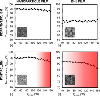
UV–vis transmittance plots of (a) PDPP-TNT:PC71BM NP film, (b) PDPP-TNT:PC71BM BHJ film (spin-cast from chloroform), (c) P3HT:PC61BM NP film, and (d) P3HT:PC61BM BHJ film (spin-cast from chloroform) exposed to a heating regime of 40 °C to 160 °C. Transmittance is a result of not only material absorption and film morphology (scattering), but also film thickness. Film thicknesses were: (a) 130 nm, (b) 225–230 nm, (c) 100 nm, and (d) 100 nm. The red shading in (c) and (d) indicates the temperature range where P3HT:PC61BM films enter a regime in which the morphology can quickly become non-optimal as the material T gs have been passed. The insets in (a) and (c) are SEM of the NP films prior to thermal treatment (1 × 1 µm2 area), and the insets in (b) and (d) are AFM height maps of the BHJ films prior to thermal treatment (1 × 1 µm2 area).

In comparison, semiconducting material NPs have the immediate advantage of allowing the morphology optimization to be decoupled from the solution casting stage of solar cell fabrication, in addition to enabling the photoactive layer to be printed from eco-friendly water-based inks. This is because the D–A domain sizes are pre-determined by the NP size, prior to casting the photoactive layer.[ Reference Holmes, Ulum, Sista, Burke, Wilson, Stefan, Zhou, Dastoor and Belcher 6 , Reference Holmes, Nicolaidis, Feron, Barr, Burke, Al-Mudhaffer, Sista, Kilcoyne, Stefan, Zhou, Dastoor and Belcher 15 ] The donor and acceptor domains in the PDPP-TNT:PC71BM NPs studied in this paper are approaching the exciton diffusion length in size (20–50 nm PDPP-TNT-rich NP shells and 50–110 nm PC71BM-rich NP cores) and can be further reduced by decreasing the NP size. The connected nature of the PDPP-TNT-rich NP shells following sintering is ideal for facilitating hole transport to the anode, while the small fraction of PC71BM in the NP shells (15–30%) facilitates the transport of electrons through the bulk film to the cathode.
Morphological stability of blend films to thermal stress
The thermal stability of an organic semiconductor blend film is critical for its long-term use. Gradual evolution of the film nanostructure through phase separation and/or crystallization during operation is likely to affect the OPV device performance.[ Reference Müller 11 ] If the material glass transition temperature (T g) of the polymer:fullerene blend system is below the standard operating temperature of the solar cell, a change in blend film morphology is possible during operation, such as gross phase separation and the growth of micrometer-sized fullerene aggregates for binary systems of low thermodynamic miscibility. The T g of organic semiconductor materials is often considered when choosing suitable thermal annealing conditions for the optimization of D–A blend film morphology, but the T g must also be considered relative to the maximum operating temperature of OPVs, which is reported to be 85 °C.[ Reference Reese, Gevorgyan, Jørgensen, Bundgaard, Kurtz, Ginley, Olson, Lloyd, Morvillo, Katz, Elschner, Haillant, Currier, Shrotriya, Hermenau, Riede, Kirov, Trimmel, Rath, Inganäs, Zhang, Andersson, Tvingstedt, Lira-Cantu, Laird, McGuiness, Gowrisankerm, Pannone, Xiao, Hauch, Steim, DeLongchamp, Rösch, Hoppe, Espinosa, Urbina, Yaman-Uzunoglu, Bonekamp, van Breemen, Girotto, Voroshazi and Krebs 12 ]
Although there are conflicting measurements of the T g of P3HT,[ Reference Hopkinson, Staniec, Pearson, Dunbar, Wang, Ryan, Jones, Lidzey and Donald 27 ] the value is generally accepted to be around room temperature. The T g of PDPP-TNT is ~85 °C.[ Reference Vaughan, Williams, Holmes, Sonar, Dodabalapur, Dastoor and Belcher 7 ] Note though that the T g of polymers can vary somewhat with molecular weight.[ Reference Müller, Wang, Andersson, Tvingstedt, Zhou, Andersson and Inganäs 28 ] The T g of PC61BM is reported to be 131 and 163 °C for PC71BM.[ Reference Müller 11 ] In addition, for two finely mixed materials only one T g (intermediate between that of the individual components) will exist. This case is observed for a 1:1 P3HT:PC61BM BHJ blend film cast from solvent, which is finely mixed, hence exhibiting a single T g in the temperature range 40–60 °C.[ Reference Müller 11 , Reference Hopkinson, Staniec, Pearson, Dunbar, Wang, Ryan, Jones, Lidzey and Donald 27 , Reference Bruner, Novoa, Dupont and Dauskardt 29 ]
An investigation of the relative thermal stability of four material films, namely PDPP-TNT:PC71BM NP, PDPP-TNT:PC71BM BHJ (spin-cast from chloroform solution), P3HT:PC61BM NP, and P3HT:PC61BM BHJ (spin-cast from chloroform solution), was undertaken using the method reported by Lindqvist et al.[ Reference Lindqvist, Wang, Andersson and Müller 30 ] (procedure detailed in Electronic Supplementary Information). Here the UV–vis transmission of each film is measured while heating from 40 to 160 °C and phase separation resulting in large fullerene aggregates is signaled by an increase in optical scattering and consequent reduction in transmitted light. The transmission plots for the four material films are presented in Fig. 4 (with full optical spectra of the material films at the initial thermal treatment (40 °C) and following the final thermal treatment (160 °C) available in Electronic Supplementary Information—Fig. S3). The P3HT:PC61BM NPs were prepared in a similar manner to the PDPP-TNT:PC71BM NPs, with the method reported in our previous paper[ Reference Holmes, Nicolaidis, Feron, Barr, Burke, Al-Mudhaffer, Sista, Kilcoyne, Stefan, Zhou, Dastoor and Belcher 15 ] and summarized in the Electronic Supplementary Information for this paper. For the PDPP-TNT:PC71BM BHJ film [Fig. 4(b)] the UV–vis transmission was relatively invariant over the temperature range applied, indicating that the film is resistant to morphological degradation, as there is little to no increase in light scattering commonly attributed to the formation of micron-sized PCBM crystallites. A slight systematic decrease in transmittance is observed above ~120 °C for the PDPP-TNT:PC71BM NP film [Fig. 4(a)]; however, no concomitant change in NP morphology is observed in the microscopy. At higher temperatures [130 °C (Fig. 1) and 150 °C (Fig. 2)] we do observe the gradual formation of small features on the Si3N4 substrate upon heating, which we hypothesize is due to the aggregation of surfactant; resulting in the observed minor decrease in transmission. Overall these results are in agreement with the STXM and electron microscopy data presented in Figs. 1–3 for the PDPP-TNT:PC71BM NP system, where no morphological degradation was observed for the various thermal annealing treatments applied.
By contrast, for the P3HT:PC61BM material system significant reductions in transmission are observed for both the NP and BHJ films upon heating. In the case of the P3HT:PC61BM NP film [Fig. 4(c)], a systematic reduction of transmittance is observed from 110 °C which accelerates from approximately 130–140 °C. For the corresponding BHJ film [Fig. 4(d)], we observe a slight systematic decrease in transmittance from 40 to 110 °C. At 110 °C the rate of the decrease in transmittance increases until a total reduction of ~7% is observed at 160 °C [Fig. 4(d)] with optical microscopy confirming the formation of Micron-sized fullerene aggregates.
When comparing the PDPP-TNT:PC71BM results to that of the P3HT:PC61BM material system we hypothesize that the latter is less stable due to the lower T g of both P3HT and PC61BM compared with that of PDPP-TNT and PC71BM. Although there are several factors that affect morphological evolution in these thin films (such as relative crystallinity of the two fullerenes), for the temperature range investigated here (40–160 °C), many of these factors (such as PC71BM crystallization) are not activated until the T g of PC71BM (163 °C) is exceeded (e.g., the temperature required for crystallization in PC71BM). As such, we speculate that T g is an important activation threshold for morphological evolution in these complex thin films. This concept is further strengthened by the fact that the inferior stability of the P3HT:PC61BM BHJ film compared with that of the P3HT:PC61BM NP film can be attributed to a blend Tg of the BHJ film of 40–60 °C.[ Reference Müller 11 , Reference Bruner, Novoa, Dupont and Dauskardt 29 ] Thus, for the temperature range explored here, the BHJ system very quickly becomes mobile (rubbery state) and gross phase separation occurs. By contrast, the P3HT:PC61BM NP film is not finely mixed as it is comprised fullerene-rich core domains and polymer-rich shell domains[ Reference Holmes, Nicolaidis, Feron, Barr, Burke, Al-Mudhaffer, Sista, Kilcoyne, Stefan, Zhou, Dastoor and Belcher 15 ] and hence does not exhibit a single low blend T g.[ Reference Holmes, Marks, Kumar, Kroon, Barr, Nicolaidis, Feron, Pivrikas, Fahy, Diaz de Zerio Mendaza, Kilcoyne, Müller, Zhou, Andersson, Dastoor and Belcher 31 ] Therefore, the onset of gross phase separation for the P3HT:PC61BM NP system will be at a higher temperature than for the BHJ system. Moreover, the semicrystalline nature of the P3HT in the shells of the P3HT:PC61BM NPs [evidenced by P3HT vibronic peaks[ Reference Holmes, Ulum, Sista, Burke, Wilson, Stefan, Zhou, Dastoor and Belcher 6 ] in the UV–vis spectrum Fig. S3(c)–40 °C] further stabilizes this system, as only the amorphous, disordered polymer fraction in the NP shells will display a glass transition.[ Reference Müller 11 ] By contrast, the absence of any vibronic structure in the P3HT component of the UV–vis spectrum for the P3HT:PC61BM BHJ film following the 40 °C thermal treatment [Fig. S3(d)] provides strong evidence that this film is mixed on a fine scale, with no crystalline P3HT domains. The blend T g of this BHJ film is then passed quickly and micron-sized fullerene aggregates grow, resulting in the reduced transmittance [Fig. 4(d)], and the P3HT forms crystalline domains, evidenced by the appearance of strong P3HT vibronic peaks in the UV–vis spectrum measured after the final thermal treatment at 160 °C [Fig. S3(d)]. Indeed, it is clear from the UV–vis spectra in Fig. S3 that for the four film types, the P3HT:PC61BM BHJ film underwent the most change during the thermal treatment regime.
Overall this is a promising result for the PDPP-TNT:PC71BM NP material system, showing that the nanoscale domain size established pre-film deposition is stable to morphological degradation at standard OPV operating conditions. Furthermore, these results reveal that for the P3HT:PC61BM system the NP films are more thermally stable than their BHJ counterparts, most importantly at the standard maximum operating conditions (85 °C). The results indicate that nanoparticulate material systems offer potential for the fabrication of thermally stable OPV devices and highlight the relevance of material T g and domain composition to material stability.
Supplementary material
The supplementary material for this article can be found at https://doi.org/10.1557/mrc.2017.3.
Acknowledgments
The authors thank the University of Newcastle Electron Microscopy and X-ray Unit. Special thanks to Robin Arnold and Samson Dowland at the University of Sydney (Anatomy and Histology, School of Medical Sciences) where TEM measurements were performed. The University of Newcastle and the Australian Renewable Energy Agency (ARENA) are gratefully acknowledged for PhD scholarships (NH). We acknowledge financial support from the Commonwealth of Australia through the Access to Major Research Facilities Program. The A.L.S. is supported by the Director, Office of Science, Office of Basic Energy Sciences, of the U.S. Department of Energy under Contract No. DE-AC02-05CH11231. This work was performed in part at the Materials node (Newcastle) and the Queensland node of the Australian National Fabrication Facility (ANFF), which is a company established under the National Collaborative Research Infrastructure Strategy to provide nano- and microfabrication facilities for Australia's researchers.