I. INTRODUCTION
Intermetallic clathrates are promising materials for thermoelectric applications. This is not only due to their low thermal and high electrical conductivities (phonon glass–electron crystal) but also due to the expectation that they are semiconductors and thus have large thermopower values. Band structure calculations of the stoichiometric compound Ba8Ga16Ge30 yield a semiconducting ground state.Reference Madsen, Schwarz, Blaha and Singh1 With conventional melting methods, however, such a state could not be realized. Metallike n-type samples are typically obtained instead.Reference Norihiko, Kishida, Tanaka and Inui2 P-type polycrystalline samples could only be produced with ball milling and spark plasma sinteringReference Bertini, Billquist, Bryan, Christensen, Gatti, Holmgren, Iversen, Mueller, Muhammed, Noriega, Palmqvist, Platzek, Rowe, Saramat, Stiewe, Stucky, Svensson, Toprak, Williams and Zhang3 and p-type single crystals by growth from Ga flux.Reference Anno, Hokazono, Kawamura, Nagao and Matsubara4
Here we use the melt spinning technique, which was discovered only recently to be applicable for the synthesis of cage compoundsReference Prokofiev, Paschen, Sassik, Laumann and Pongratz5, Reference Paschen, Gspan, Grogger, Dienstleder, Laumann, Pongratz, Sassik, Wernisch and Prokofiev6 to obtain Ba8Ga16−xGe30+x in a metastable state. This enables a smooth variation of x and hence a smooth crossover between n- and p-type conduction. It is interesting that the thermal conductivity differs drastically for these two kinds of samples. N-type samples show crystalline behavior, and p-type samples show characteristics of amorphous solids.
Currently the melt spinning technique is being used for a number of other thermoelectric materials, for example, skutterudites, Bi2Te3, and PbTe.Reference Li, Tang and Zhang7–Reference Ebling, Jacquot, Jägle, Böttner, Kühn and Kirste9 The interest for large scale thermoelectric applications is the much faster and thus less energy consuming process of melt spinning compared to conventional synthesis techniques. In the case of clathrates, typical annealing times of several weeks can be replaced by the melt spinning process of a few minutes.
II. EXPERIMENTAL
High purity elements (Ba 99.95%, Ga 99.9999%, Ge 99.9999%) were used to prepare samples of the nominal compositions Ba8Ga16−xGe30+x with x = −0.1, 0, and 0.1, by high-frequency melting of the elements in a water cooled copper boat. The premelt was then put into a quartz nozzle to perform melt spinning with the same setup as in Refs. Reference Prokofiev, Paschen, Sassik, Laumann and Pongratz5 and Reference Paschen, Gspan, Grogger, Dienstleder, Laumann, Pongratz, Sassik, Wernisch and Prokofiev6. In this process we inject the melt with a pressure of 300 mbar on a rotating copper wheel with a rotational speed of 1500 rpm. All steps were performed under a protective high purity Ar (99.999%) atmosphere.
The resulting polycrystalline flakes have a thickness of about 20 μm. They were investigated by x-ray powder diffraction, scanning electron microscopy (SEM), energy dispersive x-ray (EDX) analysis in a SEM, and, after ion milling the thinned samples, a transmission electron microscopy (TEM) apparatus (Tecnai TEM-STEM) equipped with high angle annular dark field (HAADF) and EDX detectors.
All measurements were performed directly on the melt spun flakes in a temperature range from 4 K to room temperature. The electrical resistivity and Hall coefficient were measured in a Physical Properties Measurement System from Quantum Design with a standard 4-point ac method. Thermal conductivity was measured by a steady state heating method on a melt spun flake mechanically stabilized with a layer of stycast 1266.
III. RESULTS
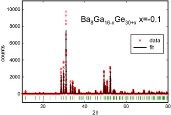
The x-ray patterns (Fig. 1) of all samples show no crystalline foreign phases. The main peaks do not show any broadening. A Scherrer analysis of the x-ray pattern confirms that the typical grain size is larger than 100 nm.
X-ray pattern and fullprof fit of Ba8Ga16−xGe30+x with x = −0.1.

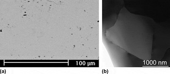
No single grains could be resolved in SEM/EDX measurements [Fig. 2(a)]. Therefore, we performed TEM investigations to describe the microstructure of the melt spun samples. The grains have a typical size of 1 μm [Fig. 2(b)]. Between the grain boundaries, at some places, nanoscale inclusions can be found (Figs. 3–5).
Typical (a) SEM/EDX and (b) TEM pictures of Ba8Ga16−xGe30+x with x = −0.1.

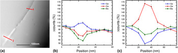
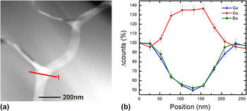
(a) HAADF picture and STEM/EDX line scans across a grain boundary of Ba8Ga16−xGe30+x with x = 0 at positions (b) 1 and (c) 2 indicated in panel (a). (b) A grain boundary without an inclusion. The small variation of the elemental composition is attributed to a change in the radiation yield due to a reduced thickness at the grain boundary. (c) A Ga rich inclusion. The error bars result from the relative error of the instrument.

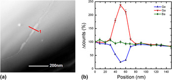
HAADF picture and STEM/EDX line scan across an impurity-containing grain boundary of Ba8Ga16−xGe30+x with x = −0.1. The error bars result from the relative error of the instrument.

HAADF picture and STEM/EDX line scan across an impurity-containing grain boundary of Ba8Ga16−xGe30+x with x = 0.1. The error bars result from the relative error of the instrument.

The STEM investigations reveal that these inclusions are rich in Ga [Figs. 3(c), 4(b), and 5(b)]. However, their total amount is very small and does not affect the total composition of the samples appreciably. Furthermore, most of the grain boundaries do not show any inclusions [Fig. 3(b)] and therefore are not expected to influence the transport properties at all.
According to the Zintl concept,Reference Schäfer10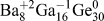 should be semiconducting. Each Ge atom is covalently bonded to four other Ge or Ga atoms. Ga has one valence electron less than Ge. This missing valence electron is formally donated by Ba to the framework, leaving a Ba+2 ion behind. Thus, by partially substituting Ga with Ge it is possible to control the number and sign of the charge carriers. Small substitutions x lead to sizable changes of the physical properties. To determine the actual compositions of the clathrate phases as precisely as possible, we used a standard in our STEM/EDX analysis: for each sample, a large scale result averaging over numerous grains was associated with the nominal composition. The results of these measurements (Table I) reveal that, within experimental resolution, the measured composition is the same as the initial composition for all three samples. The lattice parameter does not show an appreciable doping dependence.
Nominal substitution (x nom) of Ba8Ga16−xGe30+x and measured composition of the investigated samples, their lattice parameter (a), calculated (n Zintl) and measured (n Hall) charge carrier concentration at 4K, as well as charge carrier concentration derived from thermopower data (n therm)

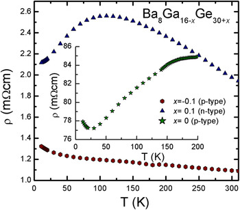
The temperature dependent electrical resistivities ρ(T) of all three  samples show the behavior typical of a degenerate semiconductor (Fig. 6). For samples with x = −0.1 and 0.1, ρ(T) assumes values of similar magnitude. However, the x = 0 sample has a much higher resistivity (Fig. 6, inset).
Temperature dependence of the electrical resistivity of Ba8Ga16−xGe30+x.

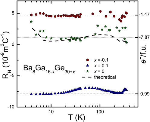
For all three samples the Hall coefficient R H (Fig. 7) is smaller than expected from the above mentioned Zintl count. In particular, the R H for x = 0 is very low. This can be understood within a two-band model for R H,
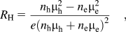
Temperature dependence of the Hall coefficient of Ba8Ga16−xGe30+x.
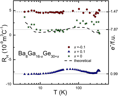
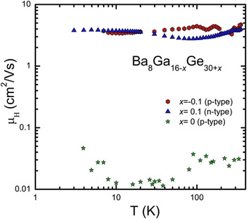
with an electron band (with charge carrier concentration n e and mobility μe) and a hole band (with n h and μh). Such a model is consistent with band structure calculations.Reference Madsen, Schwarz, Blaha and Singh1 Using the mobilities and the charge carrier concentrations of the x = −0.1 and 0.1 samples for the p- and n-type band, respectively, we calculate the dashed curve in Fig. 7. It agrees surprisingly well with the R H data for the x = 0 sample. This indicates that Ba8Ga16−xGe30+x samples with x ≈ 0 are semiconductors close to compensation. They will not be good thermoelectric materials because the presence of both p- and n-type charge carriers of similar quantity and mobility leads to cancellation effects of the thermopower, as is confirmed below. In addition, it results in a very low effective Hall mobility, as was observed experimentally (Fig. 8).
Temperature dependence of the single-band Hall mobility of Ba8Ga16−xGe30+x.

The small observed discrepancies between x Hall and x Zintl for the x = −0.1 and 0.1 samples of about 1 carrier/f.u. (see Table I) could be due to the presence of two types of charge carriers even in these samples. This option was discarded in our simple above analysis for the x = 0 sample.
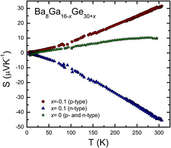
The thermopower is shown in Fig. 9. The room temperature absolute value of the x = 0.1 sample is 30% smaller than for x = 0.1, which is in good agreement with the resistivity and Hall effect data. The room temperature value is -45 μV/K for x = −0.1 and 31 μV/K for x = −0.1. Using band structure calculations,Reference Madsen, Schwarz, Blaha and Singh1 this leads to 0.6 e−/f.u. for x = 0.1 and to -1.9 e−/f.u. for x = −0.1 (Table I).
Temperature dependence of the thermopower of Ba8Ga16−xGe30+x.

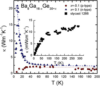
Thermal conductivity data are provided in Fig. 10. The melt spun flakes had to be mechanically strengthened with a thin layer of a low thermal conductance glue (stycast 1266) to perform steady state thermal conductivity measurements. A pure stycast sample was also measured (inset of Fig. 10), and its contribution to the measurement of the “composite” (flake plus glue) was subtracted. Radiation losses were corrected for after this subtraction. The thermal conductivity of the n-type sample clearly shows a large maximum below 40 K, which is attributed to the freezing of Umklapp scattering upon decreasing the temperature. This maximum is completely suppressed in the p-type sample.
Temperature dependence of the thermal conductivity of Ba8Ga16−xGe30+x. The insert shows the thermal conductivity of stycast 1266.

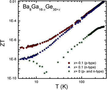
The resulting dimensionless thermoelectric figure of merit ZT (Fig. 11) is comparable for x = −0.1 and 0.1 but tiny for x = 0. Below about 11 K, a change from p-type to n-type conduction is seen for the x = 0 sample.
Temperature dependence of the dimensionless thermoelectric figure of merit of Ba8Ga16−xGe30+x.

IV. CONCLUSION
We have shown that the melt spinning technique is suitable to produce high quality Ba8Ga16−xGe30+x clathrates. Moreover, it allows us to vary x continuously from negative to positive values and thus to produce both n- and p-type materials. Together with the time and cost savings of the melt spinning technique, this presents an important step toward the commercialization of clathrates as materials for thermoelectric applications.
ACKNOWLEDGMENTS
We are grateful to S. Schwarz for TEM investigations and to the Austrian Science Foundation (FWF Project No. P19458) for financial support.