I. INTRODUCTION
Power amplifiers (PAs) for modern digitally modulated signals (e.g. QAM, PSK) demand high linearity. The required back off from maximum output power leads to a significant decrease in efficiency. Class-A amplifiers typically achieve an average efficiency of only 10% when driven with such signals. Class-B amplifiers behave slightly better but are also far from acceptable performance. Several efficiency enhancement techniques have been proposed: envelope tracking and envelope elimination and restoration [Reference Hannington, Chen, Asbeck and Larson1] apply bias modulation and require complicated modulators. Doherty amplifiers [Reference Doherty2] reactively combine the output power of a main and a peaking amplifier. Both amplifiers contribute to the output at high power levels. If the output power decreases the peaking amplifier, which typically operates under class-C conditions, shuts down and ceases to consume supply power at an accurately defined threshold. Thus efficiency is significantly enhanced at low output powers. The peaking amplifier leads to a load modulation of the main amplifier via the impedance inverter used for power combining. This deliberate active load pulling results in non-trivial design of the output networks of both amplifiers.
Recently so-called sequential power amplifiers (SPAs) [Reference Cripps3] and also switched sequential amplifiers (SSAs) [Reference Lehmann, Hettstedt and Knoechel4–Reference Lehmann and Knoechel6] were proposed as another possible choice of efficiency enhancement technique. SPAs and SSAs can be considered as a modification of balanced amplifiers. They combine two amplifiers, which also serve as main and peaking amplifiers. Both amplifiers, however, and in contrast to the Doherty amplifier, are independent of each other. No load modulation takes place.
In this paper the concept of SSAs will be extended from two channels to multi-channel operation. Design principles will be outlined and the theoretical and experimental performance of multi-channel sequential amplifiers will be discussed with respect to overall efficiency.
II. SSA DESIGN
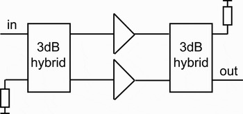
As is well known, the ordinary balanced amplifier (Fig. 1) incorporates two equal amplifiers driven in parallel via 3 dB signal splitters and combiners. By properly tracing the signal flow in this circuit it is observed that a signal supplied to the input port is first directed to both amplifiers, then amplified, and finally recombined at the lower output of the second hybrid cross over to the input. Because of the phase characteristics of the hybrids both amplifiers are decoupled. The efficiency of this balanced configuration is, apart from the loss in the couplers, the same as that of the individual amplifiers.
Ordinary balanced amplifier configuration.

Efficiency can be enhanced by switching off one of the amplifiers, thus increasing the drive of the other, if only low output power is required. This can be achieved by using switched couplers instead of the ordinarily used hybrids in the balanced configuration, thus arriving at an SSA.
A) Switched directional couplers
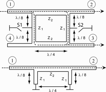
Three types of switched directional couplers were proposed in [Reference Lehmann, Hettstedt and Knoechel7]. In Fig. 2 a switched branch-line coupler is shown. This directional coupler has two operating states. In the normal state (both switches open) the coupler behaves as an ordinary branch line coupler and distributes the input power of port 1 to ports 2 and 3. The switches do not disturb the ordinary coupling behavior. If both switches are closed (bypass state) the coupler is disconnected into two perfectly matched and decoupled transmission networks between ports 1 and 2 and ports 4 and 3. A switched coupler can also be realized with so-called left-handed transmission lines (LHTL) by applying a pi- or T-circuit of lumped series capacitors and shunt inductors instead of microstrip transmission lines in the branches. Then the power distribution is the same as for the ordinary branch-line coupler but an opposite phase behavior at the output ports appears. The switched branch-line couplers (ordinary or LHTL) yield a relative bandwidth of about 5%.
Upper picture: Branch-line coupler with two open switches; lower picture: branch-line coupler with switches closed.

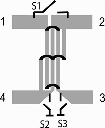
A more wideband operation is achieved by the switched Lange coupler. This type of switched directional coupler is depicted in Fig. 3. In the ordinary folded Lange coupler design three switches are inserted, one directly between ports 1 and 2 and two between ports 3 and 4 and ground, respectively. For normal coupling operation all switches are open and do not disturb the signals. In the bypass state the three switches are closed. The resulting short circuits at ports 3 and 4 are transformed over the quarter wave length longitudinal coupler dimension into open circuits at the location of the first switch, which directly connects ports 1 and 2. For the switched Lange coupler a relative bandwidth of nearly 50% was demonstrated.
Schematic of switched Lange coupler.

For both types of switched couplers the amplifiers are still embedded in a 50 Ω system for all switching states.
B) Two-channel SSA
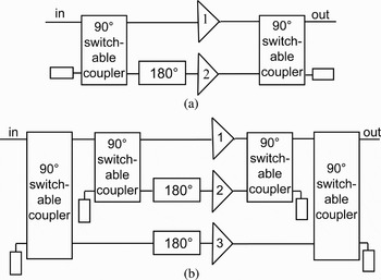
An example for a two-channel SSA using switched Lange couplers is shown in Fig. 4(a). Both amplifiers are operated in class-B or class-AB. No class-C operation of the peaking amplifier is required. To achieve a signal output directly opposite to the input port for both switching states, an additional 180° phase shift has to be inserted into the lower amplifier path. At high output power, the switches are open. Both couplers are in normal coupling state. The network behaves like an ordinary balanced amplifier apart from the change of the output port. Closing the switches turns both couplers into bypass state. Only amplifier 1 (the main amplifier) is on. Amplifier 2 (the peaking amplifier) is off and thus saves supply power. The drive power of amplifier 1 increases by the amount which had driven the peaking amplifier before, thus keeping the power gain constant. It is also possible to use an LHTL branch line coupler as the signal splitter and a switched ordinary branch line coupler as the combiner, respectively. Then an additional 180° phase shifter is obsolete, due to the opposite phase behavior of these couplers.
Switched sequential amplifier configuration. (a) Two-stage switchable network, (b) three-stage switchable network.

The switching between the two states of a two-channel network may be carried out with signal envelope speed. PIN diode switches have appropriate switching speed for this application [Reference Lehmann, Hettstedt and Knoechel4]. Maximum output powers of the main and peaking amplifier can be different. They can be fully combined if the coupling factors for the splitter and combiner are chosen appropriately.
C) Multi-channel SSA
By extending the so-far presented SSA with two additional couplers and another 180° phase shift, a three-channel SSA is composed, as shown in Fig. 4(b). This network has now three switching states where three, two, or one of the amplifiers are active. The unused amplifiers are switched off for saving supply energy. Clearly the concept can be extended in principle to even more channels.
Both types of SSAs have in common that the instantaneous output power is not changing with the switching state, but its distribution among the amplifiers. Only the necessary number of amplifiers is on. Obviously all amplifiers are required for maximum output power.
III. EFFICIENCY CALCULATIONS AND NETWORK PARAMETERS
Ordinary linear amplifiers achieve maximum efficiency only at maximum output power. If output power is reduced, efficiency decreases dramatically. Calculated average power added efficiencies (PAEs) for ordinary amplifiers driven with amplitude modulated signals are in the range of 5–10%, which is obviously not satisfactorily. Efficiency enhancement techniques predominantly aim at the improvement of the back-off efficiency, i.e. the improvement of the average PAE of amplifiers driven by signals with varying amplitude. The average PAE can be expressed as

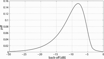
where P out is the amplifier output power, P in is the input power, P DC is the consumed amplifier supply power, η is the maximum efficiency, and pdf is the power amplitude probability density function of the signal power. To increase the average PAE of an amplifier, it is desired to adjust the maximum efficiency curve of the amplifier (e.g. SSA) to the pdf of the signal in use. A representative pdf for a typical WCDMA signal is shown in Fig. 5. The highest signal probability is at −8 dB power back-off while the probability for maximum power is small.
Typical WCDMA probability density function.

Hence, the highest possible average efficiency will be obtained if the amplifier’s maximum efficiency curve is adapted to the pdf of the applied modulated signal. For the design of the SSA and therefore the behavior of the maximum efficiency characteristics of the SSA, the coupling ratio of the signal splitter/combiner has to be devised.
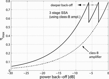
In Fig. 6 the maximum efficiency characteristics of a three-stage SSA equipped with 3 dB splitters and combiners and three ordinary class-B amplifiers as individual amplifiers in the three channels is shown. Inspection of these curves yields the following observations: starting at low powers and with decreasing power back-off, the efficiency behaves like that of an ordinary class-B amplifier until −6 dB back-off and approximately 78.5% of efficiency are reached. Up to this level only one amplifier is on and reaches its maximum output power. Couplers are in bypass state. An additional increase of output power requires a contribution of a second amplifier. Therefore, the two inner couplers are switched into normal state bringing the second amplifier into operation. This reduces the drive of the first amplifier by the amount of power coupled to the second amplifier and causes a drop in the efficiency. For this example (3 dB combiners/splitters) both amplifiers are then 3 dB below max. power. Now the output power can be increased to −3 dB back-off (both working amplifiers reach saturation). By arrival at the second efficiency peak, the remaining two outer couplers also switch to normal coupling state. Then all amplifiers contribute to the SSA output power. This behavior leads to theoretical efficiency characteristics of the SSA with three peaks at 78.5%. A −10 dB back-off efficiency of nearly 50% is obtained. The efficiency characteristics of the two-stage SSA look very similar and have only two peaks. The improvement in back-off efficiency achieved with a three-stage SSA (3 dB splitters and combiners) compared to an ordinary single class-B amplifier is 25%.
Maximum efficiency curve for a three-stage switched sequential amplifier equipped with class-B amplifiers.

By changing the coupling ratios of the used switched couplers to weaker couplings, it is possible to shift the peaks in the maximum efficiency characteristics to even deeper back-off levels. That way the back-off efficiency of the SSA can be further improved. (The weaker coupling can only be realized in practice with switched Lange couplers as splitters and combiners.) But also the power levels, where switching takes place, are important for optimizing the average efficiency. To maximize the average PAE the power levels of the occurrence of maxima and minima in the efficiency characteristics have to be optimized.
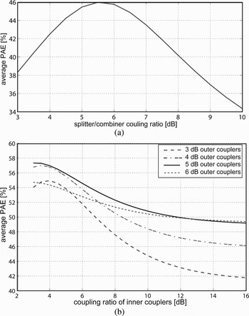
Calculations for average PAE in dependence of the given pdf (Fig. 5) were carried out. Results are depicted for two- and three-stage SSAs in Fig. 7. In Fig. 7(a) the average PAE for a two-stage network is shown. For a 5.5 dB coupling ratio of the splitter and the combiner the curve reaches its maximum of 46% average PAE. That is an improvement in the average PAE to the ordinary class-B amplifier of nearly 20% (ordinary class-B reaches only a calculated average PAE of 27.2% for the given pdf). The calculated average PAE curve is only valid for the given pdf (Fig. 5). PAE has to be recalculated for other distributions. Generally, the deeper the maximum of the power probability density function is situated in back-off, the weaker is the coupling ratio of the splitter and combiner required for a two-stage network to achieve the highest possible average PAE.
Calculated average power added efficiencies. (a) Two-channel SSA and (b) three-channel SSA.

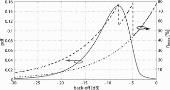
Fig. 7(b) shows a set of calculated average PAE curves for a three-stage SSA. The coupling ratio of the outer couplers is the parameter. The highest average PAE of 57% for the given pdf is achieved if 3 dB couplers as inner couplers and 5 dB couplers as outer couplers are used. This leads to an efficiency improvement of 30% compared to the ordinary class-B amplifier. Fig. 8 illustrates the effect of efficiency enhancement. The solid line shows the given pdf (Fig. 5), whereas the dashed line depicts the maximum efficiency characteristics for a three-stage SSA with 5 dB inner couplers and 3 dB outer couplers. The dash dotted line represents the maximum efficiency of an ordinary class-B amplifier. It is clearly seen that in comparison to the ordinary class-B amplifier, the maximum efficiency of the SSA is dramatically increased where the pdf indicates high probabilities of power levels. The coupling ratios of the inner and outer couplers are further adjusted to match this pdf.
Comparison: adjustment of given pdf and average PAE of three-stage SSA.

IV. SIMULATION OF SSA
To prove the concept of a multi-channel SSA, a three-channel design was simulated in detail. For this purpose a circuit as depicted in Fig. 4(b) was set up in Agilent ADS (four 3 dB couplers). To achieve realistic simulation results measured data for the signal splitter and combiner were used. Therefore, the measured scattering parameters of the built components [Reference Lehmann, Hettstedt and Knoechel7] were implemented as a four port data item. Furthermore, the PAs were designed using a GaN non-linear simulation model from Cree. As transistor the CGH40010, a 10 W device, was utilized. The different output powers of the individual PAs were obtained by proper choice of load impedances [Reference Lehmann and Knoechel8]. The PAs 1 and 2 were designed as 5 W devices by applying 100 Ω as load, while the third PA delivered 10 W with 50 Ω load impedance. The 10 W device delivered a higher gain than the others. The different gains were adjusted by applying an additional attenuator in front of the 10 W device.
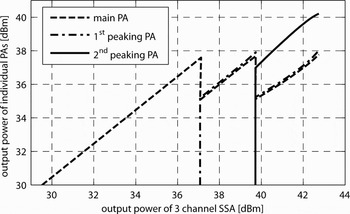
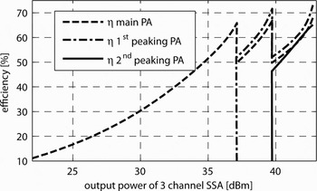
The results are shown in Figs 9–12. In Fig. 9 the output powers of the individual PAs are depicted. As can be seen, only the main PA is working up to 37.1 dBm SSA output power. Then the inner couplers are switched to coupling state and both, the main and first peaking PA, deliver nearly equal power output. The small aberration results from imperfect behavior of the signal splitter at the input (unequal signal splitting). At 39.7 dBm output power the outer couplers are also switched to coupling state and therefore all PAs contribute to the power output. Due to the losses of the signal splitter and the combiner the difference in output power when switching from one to two and three PAs is not exactly 3 dB. The corresponding efficiency of the individual amplifiers is depicted in Fig. 10. The individual PAs achieve maximum efficiencies between 66 and 72%.
Output powers of individual PAs plotted against three-channel SSA output power.

Efficiency of individual PAs plotted against SSA output power.

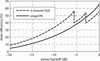
Comparison of efficiency three-channel SSA versus single PA.

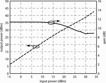
Output power and gain of three-channel SSA.

Fig. 11 shows the efficiency of the three-channel SSA in comparison to a single PA. As can be seen, the back-off efficiency is improved by 15 percentage points around −10 dB power back-off. This leads to a significant increase of average efficiency calculated in section III. The maximum efficiency values of the individual PAs are not obtained, due to the loss of the combiners; measured loss is around 0.5 dB. For that reason between −3.3 and 0 dB the back-off the efficiency of the three-channel SSA is less than that of the single PA. However, in this region the amplitude probability of most signals is negligibly small (compare Fig. 5). The output characteristics and the gain are shown in Fig. 12. The gain drops by 2 dB from 15 to 34 dBm input power. The reason is the gain characteristics of the two 5 W devices. They show unfavorable gain behavior due to the high load impedance. The gain of the SSA also shows two small spikes in the instant of switching. They are caused by gain variations and differences losses of the couplers in the individual switching states.
V. SSA LINEARITY
Linearity of the SSA depends on linearity of the used amplifiers in the different branches and the behavior of the switched splitters and combiners. Employment in an SSA does not affect the linearity of the used amplifiers, which are conventional linear amplifiers (e.g. class-B). They are decoupled and therefore could be linearized in the usual manner utilizing for example feedback or feedforward techniques [Reference Cripps3].
A closer investigation has to be devoted to distortions from the switched couplers. Two cases were investigated: A) intermodulation effects due to the couplers in fixed normal or bypass state (steady state). B) Excess distortions due to switching between normal and bypass state (transition state).
A) Steady state
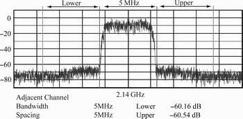
The couplers were operated in steady-state fixed positions. Reverse dc voltages (−30 V) for normal state or forward currents (30 mA) for bypass state were applied to the PIN diodes. This defines the two operating points for the diodes, which were not changed. Now, the only additional non-linearity is the intermodulation produced by the diodes. Therefore, the output signal of a single coupler in both states was measured separately, when driven with a digitally modulated signal (2.14 GHz carrier, 5 MHz bandwidth). The resulting adjacent channel power ratio (ACPR) was determined. It was better than −60 dB (Fig. 13), indicating that there are only minor distortions from the diodes.
Measured ACPR, coupler in steady state.

B) Transition state
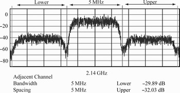
The ACPR was measured for two switched directional couplers directly interconnected without PAs. The measured distortions were only affected by the diodes and the transitions between normal and bypass state of the couplers (and vice versa). The measured spectrum is shown in Fig. 14. Only −30 dB ACPR was achieved in this measurement. Further investigations have shown that the distortions result from fabrication tolerances of the in-house fabricated switched directional couplers. The transition phase difference of the first coupler deviates by 3° in the normal state from the ideal 90° value. Also the insertion loss between normal and bypass state varies by 0.5 dB. These errors are not compensated by the second coupler, which also has fabrication tolerances. Therefore a phase and amplitude error results between the two switching states after signal combining. This error can be regarded as a kind of deterministic additional error in amplitude and phase modulation, which leads to this relatively poor ACPR. In practice, the phase and amplitude behavior of the switched directional couplers can be determined in advance and accounted for at the digital predistortion. This was successfully shown in [Reference Lehmann, Hettstedt and Knoechel4], where the ACPR was improved by 13 dB using digital predistortion with a simple look up table (LUT), where the inverse phase and amplitude information is stored. By adopting these results an ACPR in excess of −43 dB seems to be possible.
Measured ACPR, couplers in transition state.

VI. PA MEASUREMENT RESULTS
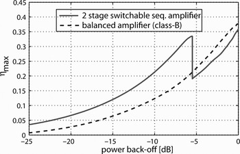
A two-channel SSA was built up utilizing 5.5 dB switched Lange couplers and two LDMOS class-B amplifiers at a design frequency of 2.14 GHz. The Lange couplers were realized on a RO4003 substrate and equipped with PIN diode switches. Measurement results are shown in Fig. 15. The dashed line denotes the efficiency of an ordinary balanced amplifier for comparison. It achieves a maximum efficiency of only 37%. This value is much less than the theoretical 78.5%, because of low efficiency of the used LDMOS transistors. It also includes the loss (5%) of the used couplers for the balanced configuration. The solid line depicts the efficiency of the two-channel SSA. The curve has the expected shape but is also shifted to lower efficiency values. That is caused by the losses (10%) of the in-house fabricated switched Lange couplers. However, the calculated average PAE of the fabricated two-stage SSA is 36%. This value is significantly higher than that of the balanced configuration (25%). The coupler loss of 10% leads to a reduction of the average PAE to 41% as compared to calculated 46% for ideal class-B amplifiers in the two-stage SSA configuration. In the three-stage SSA configuration the relative losses are somewhat higher, because there are two combing couplers at the output. Correction of the results shown in Fig. 7(b) by the losses of 10% per coupler reduces the average PAE to 47%. This is still 5% higher than what was achieved with the two-stage SSA. An SSA with more than three/four channels seems to be not advantageous, because then the combing losses are probably too high and may lead to an associated efficiency decrease (compare e.g. 11). An additional loss of 0.5 dB (additional combiner for the four-channel design) would lead to a −10% vertical shift of the SSA efficiency characteristic.
Measured results for two-stage switched sequential amplifier (solid) in comparison to a balanced amplifier (dashed).

VII. CONCLUSIONS AND OUTLOOK
A concept for multi-channel SSAs was presented. In contrast to the Doherty amplifier the PAs are decoupled. Therefore, “off the shelf” class-B or class-AB PAs can be used. The threshold between the main and peaking amplifier is introduced by the switched couplers. Class-C amplifiers are not required. Due to the decoupling, much wider bandwidths as with the Doherty amplifier may be achieved. With the three-channel SSA a −10 dB back-off efficiency of more than 50% is possible. Switching between the different SSA states can be achieved at envelope speed of digitally modulated signals. Consequently, a significant improvement from 25% (ordinary balanced configuration) to 47% average PAE for three-channel SSA can be obtained. Distortions by the switched couplers can be removed through ordinary signal predistortion.
Further investigations are in progress aiming at a two-channel SSA with couplers having variable coupling ratios. This would allow keeping the amplifier continuously at maximum output power and efficiency.
 Thomas Lehmann was born in Rostock, Germany, in 1978. He received his Dipl.-Ing. degree in electrical engineering from Christian-Albrechts-University of Kiel, Germany, in 2004. Currently he is working toward the Ph.D. degree at Microwave Laboratory of University of Kiel, Germany. His current research interests are efficiency enhancement methods for power amplifiers and especially sequential power amplifiers as well as switched sequential power amplifiers.
 Reinhard H. Knoechel received the Dipl.-Ing. in electrical engineering from the Technische Universität Braunschweig, Braunschweig, Germany, in 1975, and the Dr.-Ing. from the same university in 1980. From 1975 to 1980 he was a research assistant at the Technische Universität Braunschweig, Braunschweig, Germany. From 1980 to 1986 he was a principal scientist at the Philips Research Laboratory Hamburg, Hamburg, Germany. In 1986 he joined the Technische Universität Hamburg-Harburg, where he was a Full Professor in Microwave Electronics until November 1993. Since December 1993 he holds the Chair in Microwave Engineering with the Technische Fakultät, University of Kiel, Kiel, Germany. His research interests include active and passive microwave components, ultra-wideband technology, microwave measurement techniques, industrial microwave sensors and radar. He is a Fellow of the IEEE. He is a member of URSI Commission A, a member of the German Institute of Electrical Engineers VDE-ITG, a member of the “Microwave Committee” of VDE-ITG (Fachausschuss 7.3), and a member of the European Microwave Association (EuMA). He was recipient of the VDE best-paper award in 1978, the European Microwave Prize in 1980, and the TSH-Technology Transfer Award in 2003.