I. INTRODUCTION
The demand for touch screen panels has seen dramatic increase in applications such as mobile phones, tablets, and home appliances. It is thus of significant technological importance to develop highly sensitive touch screens. The early touch screen devices mostly rely on resistive sensing, which has several limitations. For instance, it requires physical pressing on the screen, which could cause surface damage/degradation. Reference Hecht, Thomas, Hu, Ladous, Lam, Park, Irvin and Drzaic1 More recently, devices using capacitive, Reference Hotelling and Land2 acoustic, Reference Adler and Desmares3 and infrared sensing Reference Bae, Yu, Lee, Jang, Choi, Sohn, Ahn, Kang and Chung4 have been developed. Today, the widely used commercial touch screen panels are based on projected capacitive touch technology, Reference Barrett and Omote5 owing to their durability, optical clarity, and multitouch capability.
Indium tin oxide (ITO) is the dominant electrode material used in touch screen panels due to its high conductivity and transparency. However, the brittleness, expensive vacuum-deposition process, and dwindling reserve of ITO limit its further application. Reference Hecht, Hu and Irvin6 Nanomaterials have shown promising potential as alternative electrode materials, including carbon nanotubes (CNTs), Reference Zhang, Fu, Wang, Chen, Liu, Wei, Wu, Thompson and Zhou7–Reference Wu, Chen, Du, Logan, Sippel, Nikolou, Kamaras, Reynolds, Tanner and Hebard9 graphene, Reference Tung, Allen, Yang and Kaner10–Reference Zang, Ryu, Pugno, Wang, Tu, Buehler and Zhao13 metal nanowires, Reference Hu, Kim, Lee, Peumans and Cui14–Reference Yu, Zhang, Li, Chen, Niu, Liu and Pei16 and other metal nanostructures. Wu et al. Reference Wu, Chen, Du, Logan, Sippel, Nikolou, Kamaras, Reynolds, Tanner and Hebard9 reported that single-walled CNTs show a comparable transparency and conductivity to ITO. Graphene electrodes were reported to achieve ∼30 ohms/sq and 98% optical transmittance. Reference Tung, Allen, Yang and Kaner10–Reference Wu, Agrawal, Becerril, Bao, Liu, Chen and Peumans12 Silver nanowires (AgNWs) are emerging candidates. Recently, researchers have fabricated AgNW electrodes with 20 ohms/sq and 80% optical transmittance. Reference Hu, Kim, Lee, Peumans and Cui14–Reference Yu, Zhang, Li, Chen, Niu, Liu and Pei16
Commercial touch screen panels are mainly based on hard (e.g., glass) and flexible substrates (e.g., PET). Reference Hecht, Thomas, Hu, Ladous, Lam, Park, Irvin and Drzaic1 In recent years, wearable devices have attracted significant attention. In addition to flexibility, stretchability is required to place the wearable devices comfortably on curvilinear and moving surfaces such as joints, and for them to withstand repeated mechanical deformations such as bending and twisting. Reference Kim, Lu, Huang and Rogers17–Reference Kim, Xiao, Song, Huang and Rogers20 Hence, it is of relevance to develop touch sensors on stretchable substrates. Stretchable touch sensors in the pattern of parallel-plate capacitor have been recently demonstrated. Reference Yao and Zhu21–Reference Cotton, Graz and Lacour23 However, their capacitances increase considerably with the applied strain.
In this paper, we present flexible and stretchable touch sensors with two different patterns (interdigitated and diamond-shaped capacitors – to be described later). The touch sensors were made of screen-printed AgNW electrodes embedded in polydimethylsiloxane (PDMS). For each pattern, the simulation-based design was first conducted to choose optimal dimensions for the highest touch sensitivity, followed by the fabrication of the designed sensors. The prototype sensors were characterized when undeformed and deformed (e.g., under bending and stretching) for comparison of sensor performances. The attributes of each pattern are discussed in terms of touch sensitivity and stability under bending and stretching. Note that while AgNW-based touch sensors could be transparent, this paper focuses on the flexibility and stretchability.
II. DESIGN AND OPTIMIZATION
Patterning of sensor electrodes is important to maximize the touch sensitivity as the capacitance change upon touch is typically very small, e.g., in the order of fF. The parallel-plate pattern has been used in stretchable touch sensors but its stability under tensile strain is limited. Reference Yao and Zhu21–Reference Cotton, Graz and Lacour23 In addition, it requires two layers of electrodes separated by a dielectric layer. Diamond-shaped pattern is popular due to its high sensitivity, Reference Barrett and Omote5 but it also requires two layers of electrodes and a dielectric layer in between. Reference Kim, Hong and Koo24 On the other hand, the interdigitated pattern possesses reasonable sensitivity and the two electrodes are on the same layer, which makes the whole device thinner than the other patterns. In this paper, we will investigate both the interdigitated and diamond-shaped patterns.
Finite element analysis (FEA) was carried out to design and optimize the sensor dimensions using ANSYS APDL 14.5. FEA is important here as it accounts for the fringing effect in calculating the capacitance. The elements used to define the electrodes and the media are Structural Mass Tet 187 and Electrostatic Tet 123, respectively. The dielectric constants used are 2.6 for PDMS and 1 for air, respectively. Two conductors are defined in the model to represent the two electrodes in a capacitor and the third conductor is defined for a finger (or a conducting object) that touches the capacitor. The third conductor is grounded. In the following, the interdigitated design is presented first, followed with the diamond-shaped design.
A. Interdigitated pattern
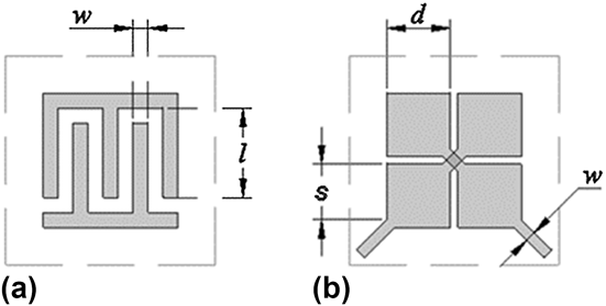
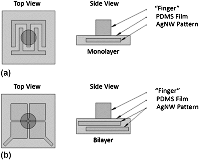
Figure 1(a) shows a schematic of the interdigitated touch sensor. The interdigitated design includes a 0.1-mm-thick layer of AgNW electrodes that are embedded in PDMS (∼0.50 mm in thickness). To optimize the touch sensitivity of the touch sensor, the dimensions of the electrode finger were varied in the simulations while the sensor footprint was maintained as 18 × 18 mm. Here the touch sensitivity is defined as the difference in capacitance between almost touch (i.e., when the finger or conducting object is 1 mm above the sensor) and direct touch (i.e., when it physically touches the sensor). Reference Lee, Cole, Lai and Nathan25 In the FEA model as shown in Fig. 2(a), an 8 mm layer of air block is included above the sensor to capture the fringe field between the sensor and the finger. A 10-mm-diametered cylinder represents the finger with a varying height (7 or 8 mm) to calculate the capacitance when the finger is 1 mm above or touches the sensor. The design objective is to achieve the highest possible touch sensitivity.
Schematic of the interdigitated and diamond-shaped touch sensors. (a) Parameters simulated in the interdigitated touch sensor including the finger length l and the finger width w. (b) Parameters simulated in the diamond-shaped touch sensor including the square size d, the middle strip width w and the effective square length s. For the bending and stretching tests, both sensors are bent and stretched in the horizontal direction. Note that the dashed lines in (a) and (b) represent the footprints of the touch sensors (the same as the PDMS matrices). Both sensors were stretched in horizontal direction.

Top and side views of the interdigitated and diamond-shaped touch sensors. (a) Simulation setup for the interdigitated sensor model. The sensor includes one layer of AgNWs. (b) Simulation setup for the diamond-shaped sensor model. The sensor includes two layers of AgNWs.

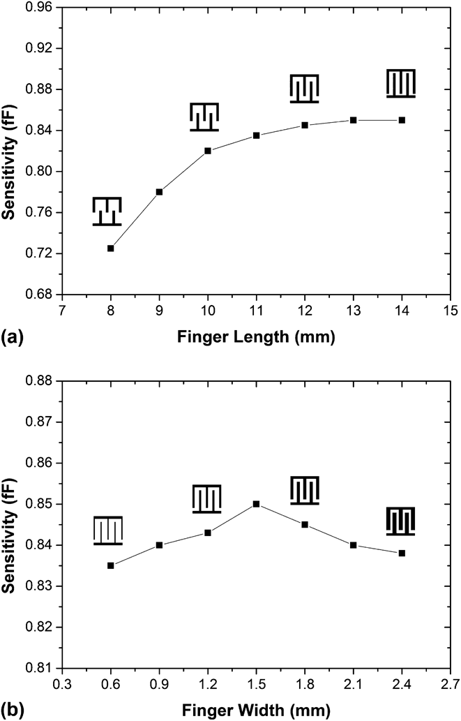
The first design parameter is the electrode finger length (l) as marked in Fig. 1(a). In this work, the finger length was varied from 8 to 14 mm (equivalent to overlap from 1 to 13 mm). As shown in Fig. 3(a), the touch sensitivity rapidly increases up to the point when the electrode finger is 10 mm long. Beyond that, the touch sensitivity shows limited increase. The touch sensitivity increases with the overlap length between the electrode fingers due to the increased fringing field. However, after the overlap exceeds the cylinder (touch finger), the change in the fringe field does not affect the touch sensitivity considerably.
Parametric study of the interdigitated touch sensor. (a) Sensitivity results based on the electrode finger length varied from 8 to 14 mm. (b) Sensitivity results based on the electrode finger width varied from 0.6 to 2.4 mm.

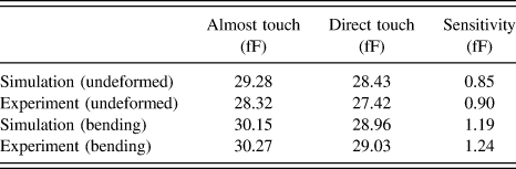
The next design parameter is the electrode finger width (w) that was varied from 0.6 to 2.4 mm. As shown in Fig. 3(b), the touch sensitivity is peaked when the width reaches 1.5 mm. During this parametric study, to keep the touch cell footprint, the spacing between the fingers reduces with increasing finger width. There is a tradeoff between the finger width and the spacing between the fingers. A wider finger leads to a more extended fringe field, which is disturbed more by the finger touch and thus a higher touch sensitivity. Reference Hammer26 On the other hand, a smaller spacing leads to a larger capacitance before finger touch and thus decreases the touch sensitivity. In the optimized sensor design, the electrode fingers are 1.5 mm wide and 13 mm long as a result of the above parametric study. For the optimized sensor dimensions, the capacitance values were 29.28 and 28.43 fF for almost touch and direct touch, respectively, with the touch sensitivity of 0.85 fF.
B. Diamond-shaped pattern
Figure 1(b) shows a schematic of the diamond-shaped touch sensor. The diamond-shaped design includes two layers of AgNW electrodes (0.1 mm in thickness each). The electrodes are embedded in PDMS and are separated by a layer of PDMS (∼0.95 mm in thickness). Similarly to what was done for the interdigitated electrode design, several dimensions of the diamond electrode were varied. During the simulations, the electrode footprint (18 × 18 mm) was kept constant. The same 8-mm-thick air block was included to simulate the device boundary and capture the fringe field around it.
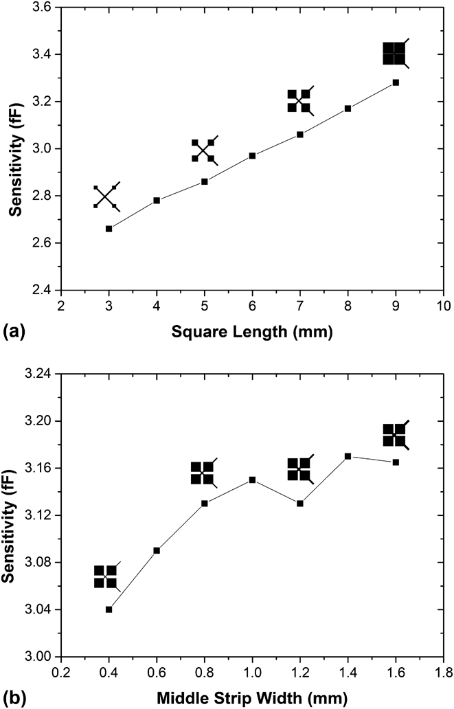
The first design parameter is the square length (d) as marked in Fig. 1(b). This dimension was varied from 3 to 9 mm. As shown in Fig. 4(a), the increase in the square dimensions leads to higher touch sensitivity. According to Lee et al., Reference Lee, Cole, Lai and Nathan25 the region between two squares of each diamond electrode concentrates the fringing field and is therefore the highly sensitive region for touch. According to Hwang et al., Reference Hwang, Cui, Yang and Kwon27 the sensitivity is proportional to the effective square length (s).
Parametric study of the diamond-shaped touch sensor. (a) Sensitivity results based on the electrode square size varied from 3 to 9 mm. (b) Sensitivity results based on the electrode middle strip width varied from 0.4 to 1.6 mm.

Next, the width of the middle strip (w) that connects the two squares in the diamond electrode was varied. As it can be seen from Fig. 4(b), the sensitivity increased initially with the middle strip width and then varied between 3.13 and 3.17 fF. According to Hwang et al., Reference Hwang, Cui, Yang and Kwon27 the touch sensitivity is directly proportional to the middle strip width and the effective square length, as mentioned before. However, the wider the middle strip the smaller the effective square length (s), which can be seen as a tradeoff.
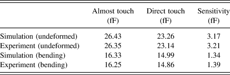
The optimized diamond pattern had a square length of 8 mm and not 9 mm because of the ease in fabrication and a central strip width of 1.4 mm. For the stipulated electrode dimensions, the capacitances are 26.43 and 23.26 fF for almost touch and direct touch, respectively, with the sensitivity of 3.17 fF.
C. Effect of touch finger size
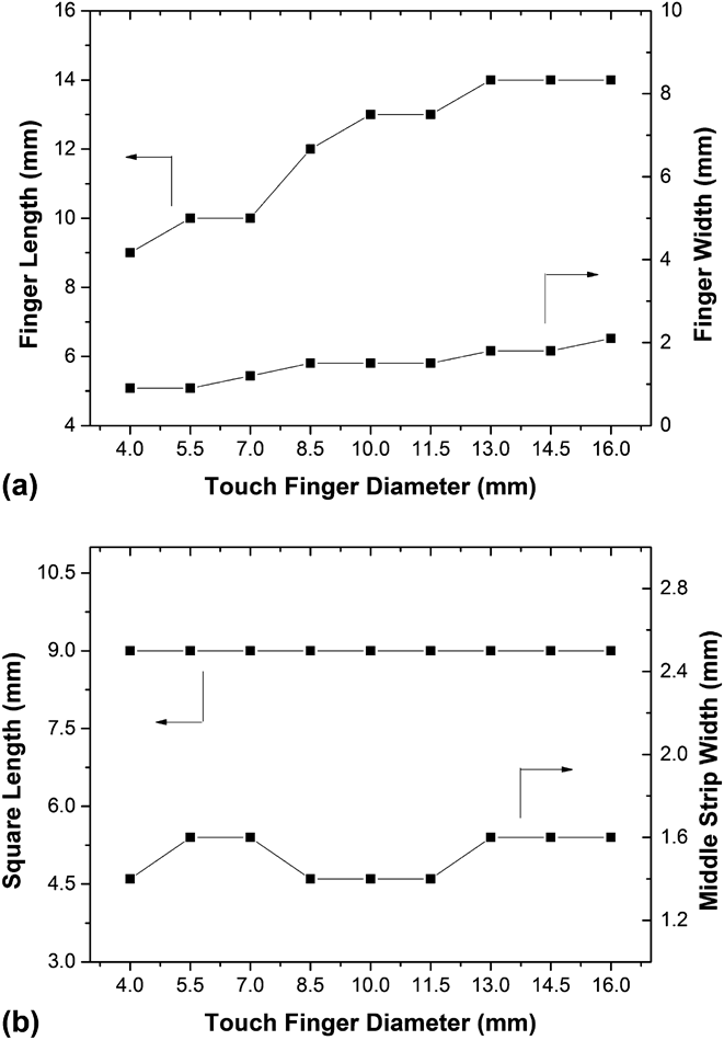
The optimized dimensions of both patterns depend on the size of the touch finger. To generalize the optimization results, the cylinder diameter used in the FEA was varied in a wide range (i.e., from 4 to 16 mm to represent a wide variation of touch finger size, for instance, from children to adults, from finger tip to finger pad, and from little finger to thumb). The electrode parameters for both designs were varied once again and the optimized dimensions were found for each finger size. Figures 5(a) and 5(b) show the results of the interdigitated design and the diamond design, respectively. In Fig. 5(a), the electrode finger length is more susceptible to touch finger size whereas the optimized electrode finger width remains nearly constant. In Fig. 5(b), the optimized middle strip width varies from 1.4 to 1.6 mm while the optimized square length remains constant. The results showed that the diamond design has a more stable performance for a range of human finger sizes when compared to the interdigitated design. In the experimental work to be described below, we will focus on the optimized designs for the 10-mm-diametered touch finger.
Optimized dimensions as functions of the touch finger diameter. (a) Optimized finger length and width for the interdigitated pattern as functions of touch finger diameter. (b) Optimized square size and middle strip width for the diamond pattern as functions of touch finger diameter.

III. FABRICATION
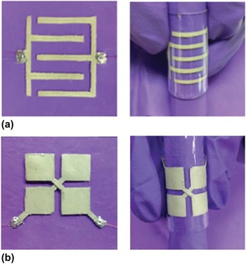
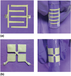
To fabricate the touch sensors, AgNW conductors with the optimized dimensions for the interdigitated and diamond patterns were screen printed on top of a Si substrate through a prepatterned PDMS shadow mask. More details on the fabrication processes of the AgNW electrodes were reported previously. Reference Xu and Zhu28,Reference Song, Myers, Adams and Zhu29 Liquid PDMS (mixing the “base” and the “curing agent” at a weight ratio of 10:1) was then cast on the Si substrate over the prepared AgNW electrodes, and cured at 100 °C for 35 min in a degassed oven. All the pattered AgNW electrodes were embedded just below the PDMS surface when the composite was peeled off from the Si substrate. Eutectic gallium–indium (EGaIN, Aldrich, ≥99.99%) liquid metal was applied to the ends of each electrode to serve as conformal electric contacts. After that, copper wires were embedded inside the liquid metal and covered by a new layer of PDMS of the same thickness, followed with a curing step. Up to this step, the interdigitated pattern sensor was fabricated. The diamond pattern was fabricated by positioning the AgNW/PDMS film (without the new layer of PDMS on top) orthogonal to another identical AgNW/PDMS film face to face with a thin layer of liquid PDMS in between, followed by a curing step. Both interdigitated and diamond-shaped sensors, as-fabricated and bent, are shown in Fig. 6.
Fabricated Ag NW touch sensors. (a) Left and right show as-fabricated and bent Ag NW interdigitated touch sensor, respectively. (b) Left and right show as-fabricated and bent Ag NW diamond-shaped touch sensor, respectively.

IV. RESULTS AND DISCUSSION
The capacitance was measured by an AD7152 capacitance-to-digital converter (CDC) evaluation board (Analog Devices), which has the offset calibration function to compensate parasitic capacitance from the lead wires and the surrounding environment. A cylindrical metal bar with a diameter of 10 mm was used as the touch finger as in the simulation. The bar was grounded to mimic the human touch. The capacitance of the interdigitated sensor cell was measured at 28.32 and 27.42 fF for almost touch and direct touch, respectively. The capacitance of the diamond-shaped sensor cell was measured at 26.35 and 23.14 fF for almost touch and direct touch, respectively. These results are in good agreement with what we obtained from the simulations.
Furthermore, the interdigitated and diamond-shaped sensors were characterized under bending and stretching. In the bending study, the sensor was wrapped around a cylinder with a radius of 6.5 mm. The capacitance of the interdigitated sensor cell was measured at 30.27 fF for almost touch, decreasing to 29.03 fF for direct touch. Compared with the interdigitated one, the diamond sensor cells showed a larger change in capacitance, dropping to 16.25 fF for almost touch and 14.86 fF for direct touch.
Table I lists the simulated and measured capacitance values for the interdigitated sensor when undeformed and bent. Both capacitances and touch sensitivity under bending do not change noticeably when compared to those when undeformed. This result shows that the capacitive sensor can maintain similar performance even when it is bent.
Capacitance values and touch sensitivity for the interdigitated sensor.

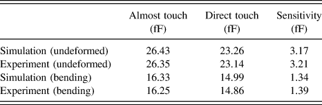
Table II lists the simulated and measured capacitance values for the diamond-shaped sensor when undeformed and bent. The diamond pattern shows a larger variation in capacitances and touch sensitivity when bent compared to the interdigitated design. Since the diamond pattern consists of two electrode layers, it might be more susceptible to capacitance changes due to the relative motion between the layers under bending. This observation is consistent with the simulation results.
Capacitance values and touch sensitivity for the diamond-shaped sensor.
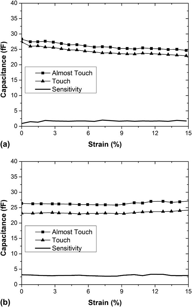
Furthermore, both types of sensors were stretched up to 15% strain. The capacitances as functions of the applied strain are shown in Figs. 7(a) and 7(b). For the interdigitated sensor, the capacitance values for both almost touch and direct touch decreased with increasing strain, but the difference between almost touch and direct touch was nearly independent of the strain, suggesting a stable sensitivity over a large range of stretching strain. The average of the capacitance difference was 0.92 fF with a standard deviation of 3.14%, which is in a good agreement with the difference of 0.90 fF when the sensor was not deformed. For the diamond-shaped sensor, the capacitance values remained almost constant up to 15% strain. The average of the capacitance difference was 2.98 fF with a standard deviation of 6.81%, which is in a good agreement with the difference of 3.21 fF when the sensor was not deformed.
Measured capacitances and touch sensitivity for touch sensors under stretching. Capacitances at almost touch and direct touch and touch sensitivity for the (a) interdigitated and (b) diamond-shaped touch sensors.

Based on the above results, the diamond-shaped pattern showed better touch sensitivity than the interdigitated one when undeformed, bent or stretched. For the interdigitated pattern, the touch causes a 3.18% decrease in capacitance when the sensor is undeformed. When the sensor is curved, it shows a decrease about 4.10% in capacitance. The undeformed diamond pattern shows an excellent performance, with a 12.18% drop in capacitance when directly touched. When the diamond sensor is curved, it still shows an 8.55% decrease in capacitance. When the two patterns are stretched, their touch sensitivities are nearly unchanged when compared to the undeformed state. On the other hand, the interdigitated pattern showed better stability than the diamond-shaped pattern. The interdigitated pattern maintained nearly the same performances when undeformed, bent or stretched, while the diamond-shaped pattern showed much decreased sensitivity under bending.
The long-term stability of the sensors is of paramount importance for wearable applications. The interdigitated and diamond-shaped sensors were tested under cyclic loading up to 15% tensile strain. The capacitances of both types of sensors remained nearly the same after 2000 cycles. Degradation of AgNW electrodes over time due to oxidation can compromise the device performance. Reference Zhang, Wong and Yuen30,Reference Lee, Lee, Roy, Lee, Park and In31 Compared to unprotected AgNW electrodes (i.e., AgNWs on top), Lee et al. found that fully embedded AgNW electrodes in PDMS kept the same resistance for a much longer period of time under UV light. Reference Lee, Lee, Roy, Lee, Park and In31 Besides, our electrodes work as capacitors, which are less prone to the resistance change of the electrodes. Hence, our touch sensors should be robust against oxidation. Indeed, our sensors showed similar performances three months after their fabrication.
The sensors presented in this paper were not transparent. Transparency is critical for wearable touch sensors. Kim et al. showed that more uniformly distributed AgNW networks with lower density are key to transparent electrodes with reasonable conductivity. Reference Kim, Kim, Lee, Kim, Yang and Suh32 In addition, as mentioned above our capacitance-based sensors are not affected much by the resistance change of the electrodes. For future work, we aim at developing transparent and wearable touch sensors with similar performances as presented here.
V. SUMMARY
Flexible and stretchable touch sensors with two different patterns (interdigitated and diamond-shaped capacitors) were designed, fabricated, and tested. The sensors were made of screen-printed AgNW electrodes embedded in the PDMS matrix. The interdigitated pattern possesses the advantage of just using one layer of AgNWs (instead of two used in the diamond-shaped pattern). The experimental and simulated results showed that the diamond pattern is more sensitive than the interdigitated one in all cases (e.g., undeformed, under bending or under stretching). For both types of sensors, the touch sensitivity remained nearly constant under stretching up to 15%, but varied under bending especially for the diamond-shaped ones. They also showed robust performances under cyclic loading and against oxidation. The demonstrated flexible and stretchable touch sensors have potential to be integrated in wearable devices. Future work would include development of larger-area, transparent, and wearable touch sensors.
ACKNOWLEDGMENT
This work was supported in part by the National Science Foundation through the ASSIST Engineering Research Center at NCSU (EEC-1160483).