I. INTRODUCTION
Nikola Tesla first experimented with wireless power in 1891, but it gained momentum and widespread interest in the 1970s [Reference Tesla1]. During this time, the very first high-efficiency rectenna, a combination of antenna and rectifier circuit used to rectify the incoming ac signal, was implemented [Reference Brown and Eves2–Reference Shinohara4]. Designs during this era constituted far-field solutions that have applications in military, space, and industries. Wireless power transfer can be categorized into three types: near-field transfer, microwave power transfer, and microwave power harvesting; among which, near-field transfer can deliver tens of watts of power using magnetic field coupling with less safety concerns and with higher efficiency. Thus, this design is aimed for near-field high-power applications. The power levels under consideration may cause interference to the large wireless traffic present at higher frequencies [5]. Therefore, 13.56 MHz is chosen as the frequency of operation.
In a radio frequency (RF) wireless power receiver, the rectifier circuit is a major contributor to the overall loss of efficiency. The RF wireless power receiver system has a receiving antenna followed by a filter-rectifier circuit to convert energy from the transmitted RF signal. Ideally, the switch used in the circuit should have no resistance, but in practice the diode used as a switch has parasitic resistance, resulting in a lower efficiency. To minimize this loss in efficiency, we describe a technique to engineer waveforms as used in switch mode power amplifiers [Reference Raab6] in this paper.
Yoshida et al. [Reference Yoshida, Tanomura and Chen7] demonstrated a high-efficiency rectifier by terminating the second-harmonic component using a series-resonant circuit. A maximum efficiency of 85% was reached at 27 dBm, but the efficiency dropped with an increase in the input power; falling to 60% at 33 dBm. Fu et al. [Reference Fu, Zhang, Zhu and Ma8] designed a wireless power system at 13.56 MHz that uses a full-wave rectifier with an efficiency of 76–81%. A high-power, high-efficiency rectifier designed by Liou et al. [Reference Liou, Lee, Huang and Mao9] uses series and parallel power division circuit to increase conversion efficiency at high-power levels. Efficiencies of 62 and 76% have been shown for the series and parallel power divider networks, respectively. Hosain and Kouzani [Reference Hosain and Kouzani10] compared several rectifier configurations to operate at 30 dBm, but none of which has an efficiency of more than 75%. Noda and Shinoda [Reference Noda and Shinoda11] used Schottky diodes in an anti-symmetric configuration to operate in Class-F configuration, achieving 78% efficiency at 27 dBm. Falkenstein et al. published a rectifier design at 2.14 GHz using a modified inverse Class-F GaN power amplifier that approached 85% conversion efficiency at 40 dBm [Reference Roberg, Reveyrand, Ramos, Falkenstein and Popovic12]. Kang et al., discussed the implementation of a high-efficiency rectifier [Reference Kang, Park, Jang and Lee13]. To achieve a high-efficiency, these designs sacrifice simplicity and ease of implementation. Several high-efficiency rectifiers have been discussed in literature, but they are low-power rectifiers operating at higher frequencies.
The novelty of the solution presented in this paper lies in the design of a robust, low-frequency, high-power rectifier for wireless charging at 1 W level. To achieve high conversion efficiency, implementation of harmonic terminations in a shunt diode rectifier is presented. The theory based on Fourier analysis as well as the design and measurment results of our existing prototype are discussed in the sections that follow.
II. BASIC ARCHITECTURE AND FOURIER ANALYSIS
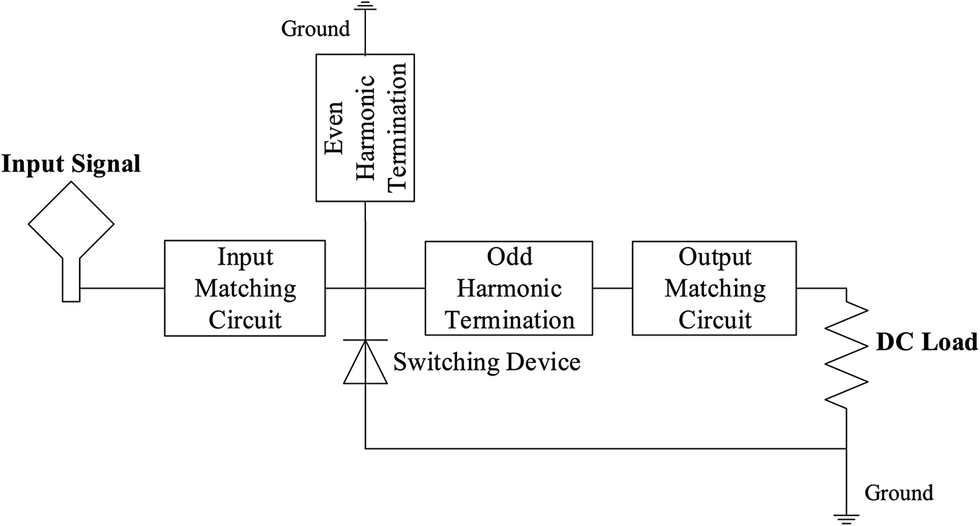
As shown in Fig. 1, the receiver chain consists of an input matching network, a switching device, harmonic terminations, an output matching circuit, and a dc load. In practice, switching elements are implemented using semiconductor devices such as transistors and diodes [Reference Roberg, Reveyrand, Ramos, Falkenstein and Popovic12]. The harmonics in the receiver circuit are analyzed by applying Fourier series expansion. Under ideal conditions, the diode behaves as a switch with resistance given by (1).
 $${R_d} = \left\{ {\matrix{ {0,} & {{\rm diode\; is\; ON,}} \cr {\infty, \;} & {{\rm diode\; is\; OFF}{\rm.}} \cr}} \right.$$
The input RF signal is represented by (2).
 $${V_i} = {V_m}\;{\rm sin}(\omega t).$$
The response of the diode connected in a shunt reverse bias configuration is represented in (3). Fourier series expansion, as explained in [Reference Raab6, Reference Roberg, Reveyrand, Ramos, Falkenstein and Popovic12] is applied to study the harmonics generated in the circuit. The transformed equations for voltage across and current through the diode are derived as (4) and (5).
 $${V_d} = \left\{ {\matrix{ {{V_m}{\rm sin(}\omega t{\rm )},} & {0 \le t \le \pi,} \cr {0,} & {\pi \le t \le 2\pi,} \cr}} \right.$$
 $${v_d} = {V_{dc}} + {V_1}{\rm cos}\,(\omega t) + {V_2}{\rm cos}\,{\rm (}2\omega t{\rm )} + {V_3}{\rm cos}\,{\rm (}3\omega t{\rm ),}$$
 $${i_d} = {I_{dc}} + {I_1}{\rm cos}\,{\rm (}\omega t{\rm )} + {I_2}{\rm cos}\,{\rm (2}\omega t{\rm )} + {I_3}{\rm cos}\,{\rm (3}\omega t{\rm )}{\rm.} $$
Voltage and current waveforms contain high-frequency harmonics that can be shaped to achieve high RF–dc conversion efficiencies. The diode's internal resistance is the main cause of power loss. However, tuned circuits can be used to terminate high frequency to shape voltage and current, forcing a zero voltage switching condition across the diode. In this paper, Class-F type of terminations is implemented where all the odd harmonic components are open-circuited and even harmonic components are short-circuited. Terminations are designed using discrete components unlike in [Reference Noda and Shinoda11, Reference Roberg, Reveyrand, Ramos, Falkenstein and Popovic12] where transmission lines were used. Transmission lines at 13.56 MHz would physically be too long, making the design inefficient and impractical.
Block diagram of a WPT receiver system.

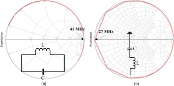
The terminations work on the concept of different impedance values seen by the harmonics. For odd harmonic terminations, a parallel LC tank, which has a reflection coefficient of one (Fig. 2(a)) is used. The circuit presents high impedance to the odd harmonic of voltage (V odd ) and reflects the signal toward the diode. Since a high impedance is present at the odd harmonics (Z odd ), Ohm's law (V odd = Z odd × I odd ) results in an infinitesimal current at odd harmonics (I odd ). Thus, the odd harmonic component of current is ideally reduced to zero.
(a) Third-order harmonic termination circuit (b) Second-order harmonic termination circuit.

The even-order harmonic termination circuit, represented by Fig. 2(b) creates low impedance and a reflection coefficient of −1 to even harmonics. Since impedance seen by even harmonic components (Z even ) is ideally zero, Ohm's law (V even = Z even × I even ) results in a zero even-order harmonic components (V even ) and reflects even harmonic component of current (I even ).
The reflection coefficients measured across the tuned circuits in the prototype are presented in Smith charts simulated using Agilent ADS. From Fig. 2 it is clear that for the third-harmonic frequency component, i.e. 40.68 MHz, the reflection coefficient is 1 (open circuit) and for the second-harmonic frequency component, i.e. 27.12 MHz, the reflection coefficient is −1 (short circuit). Therefore, the terminations are pivotal for controlling impedance of each of the harmonics to shape the voltage and current across the diode.
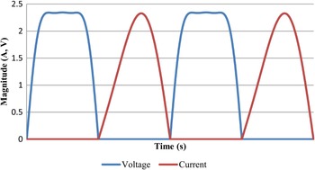
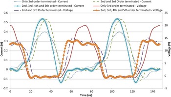
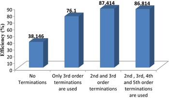
For obtaining a zero loss condition as shown in Fig. 3, all the harmonic frequency components need to be terminated. The phenomenon of waveform shaping using termination circuits is shown in this figure. Figure 4 illustrates the effect of terminations on the voltage and current waveforms across the diode when the finite numbers of harmonics are terminated. When no harmonic terminations are used, the circuit behaves like a half-wave rectifier. If only one termination is used, then the efficiency of the circuit is greater than that of the half-wave rectifier, but still does not reach an appreciable level. The circuit attains optimum efficiency when both second- and third-order harmonics are terminated. As shown in Fig. 5, if higher-order harmonics are terminated, the voltage current waveforms across the diode approaches the theoretical prediction, but the dc resistance (DCR) of the higher-order harmonic termination circuit will cause additional loss in efficiency. Moreover, the design complexity outweighs the benefits of using higher-order terminations. So, only second- and third-harmonic terminations are considered for practical implementation and prototyping.
Ideal voltage and current waveforms across the diode if all harmonics are terminated.

Voltage and current waveforms across the diode when different terminations are used.

Comparison of efficiency with number of terminations being used.

Applying this approximation to equations (4) and (5), the voltage and current across the diode are now given by (6) and (7).
 $${v_d} = {V_{dc}} + {V_1}{\rm cos}\,{\rm (}\omega t{\rm )} + {V_3}{\rm cos}\,{\rm (3}\omega t{\rm ),}$$
 $${i_d} = {I_{dc}} + {I_1}{\rm cos}\,{\rm (}\omega t{\rm )} + {I_2}{\rm cos}\,{\rm (2}\omega t{\rm )}{\rm.} $$
III. EXPERIMENT
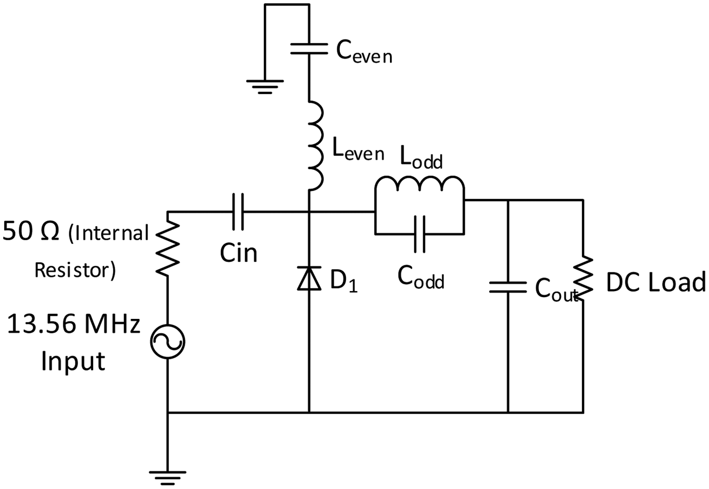
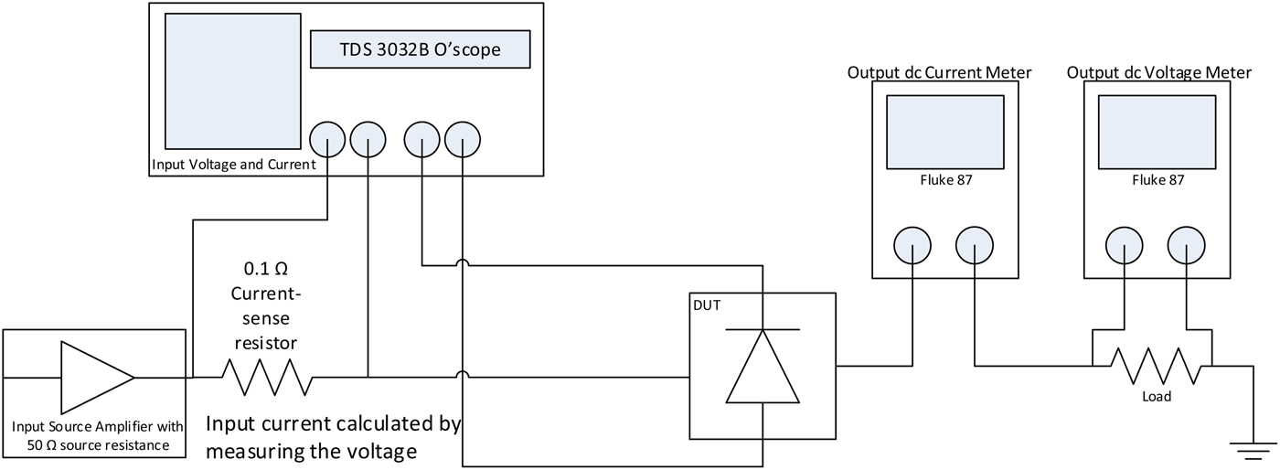
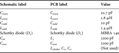
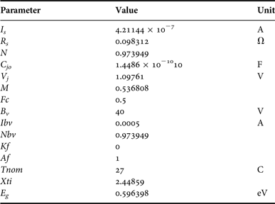
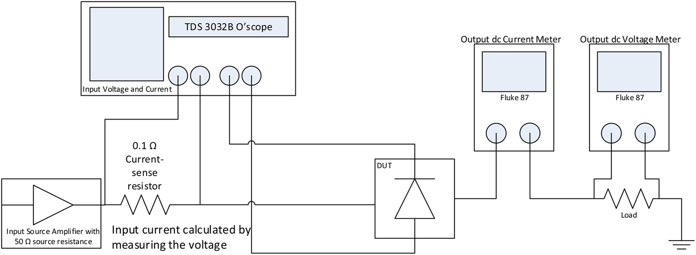
Simulations in ADS and bench tests on a shunt diode rectifier with second- and third-order harmonics terminated are performed to validate the theory discussed. The terminations built using lumped components are tuned to 27.12 and 40.68 MHz, the second- and third-harmonic frequencies, respectively. MBRA 140, is chosen as the switching device for this work, as it has a high reverse breakdown voltage (40 V), large current-handling capabilities (1 A) and a low forward voltage drop (0.55 V) (see the Appendix). The junction capacitance and resistance of this device are ~40 pF and ~98 mΩ, respectively. C in and C out form the input and output match circuits, respectively. Their values are chosen to create a power match at the source, reducing any mismatch loss. The value of C out , part of the smoothing circuit, ensures that the RC time constant of the circuit is > 1/f (τ = R load × C out ≫ 1/f). Figure 6 shows the schematic representation of the rectifier and Table 1 lists the components used for the tests performed. Simulations in ADS use the Harmonic Balance solver with the fundamental frequency set to 13.56 MHz and the order set to 7. To increase the computational accuracy of the solver, the order is set to 7 even though only 5 harmonics are analyzed. Figures 7 and 8 show the populated PCB and measurement system used to perform bench tests.
Schematic representation of the rectifier circuit.

Experimental board.

Measurement system.
Components.

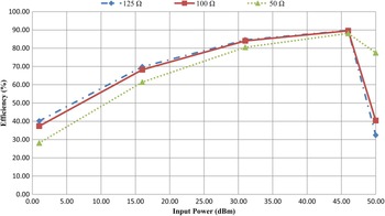
To prove the Class-F operation of this design, the load used at the output to measure voltage and currents across the diode is chosen based on simulations in ADS. It is observed that a large output impedance causes a high reverse voltage to appear across the diode, which results in a large output dc voltage. A larger load results in higher efficiency, but the diode reaches breakdown faster [Reference Guo, Zhang and Zhu14]. The circuit is simulated with several loads and the efficiencies are measured between 0 to 50 dBm. A 100 Ω load is chosen as it is a good compromise between, achieving high-efficiency and preventing the diode from reaching breakdown faster. The simulated load analysis is plotted in Fig. 9.
Simulated output versus dc load.

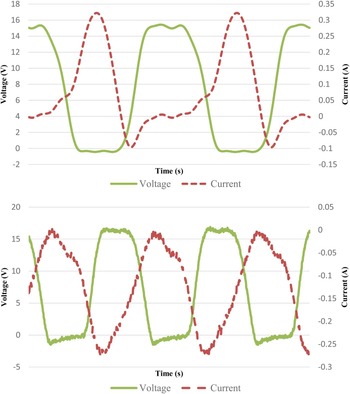
The effect of terminations is verified by analyzing voltage and current across the diode. The ratio of output dc power to the input RF power determines the conversion efficiency (η = output dc power/input RF power). From Fig. 10, it is seen that the simulation and the bench test results are in agreement of each other. The square voltage and sinusoidal current waveforms, confirm the use of terminations to improve the efficiency of the rectifier. It is seen that the measured waveforms are non-ideal representations of the Class-F waveforms. This could be an effect of the voltage reduced by the junction capacitance, C j , of the diode which is similarly explained by Guo et al. [Reference Guo, Zhang and Zhu14] in their analysis.
Simulated (top) and measured (bottom) voltage and current across the diode.

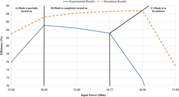
The efficiency of the circuit at different power levels is presented in Fig. 11. This graph represents the typical behavior of a harmonically terminated diode rectifier. The entire plot can be divided into three regions based on the operating point of the diode; the first being the “turn-on” region where the input power is not sufficient to completely turn ON the diode. This results in a large power loss across the diode. In the second region, the diode is ON and is operating nominally; this is also the region where the maximum rectification efficiency is obtained. Beyond this region, if a higher input power is applied, the diode enters breakdown region and may lead to device failure [Reference Guo, Zhang and Zhu14].
Efficiency comparison of experimental and simulated data.

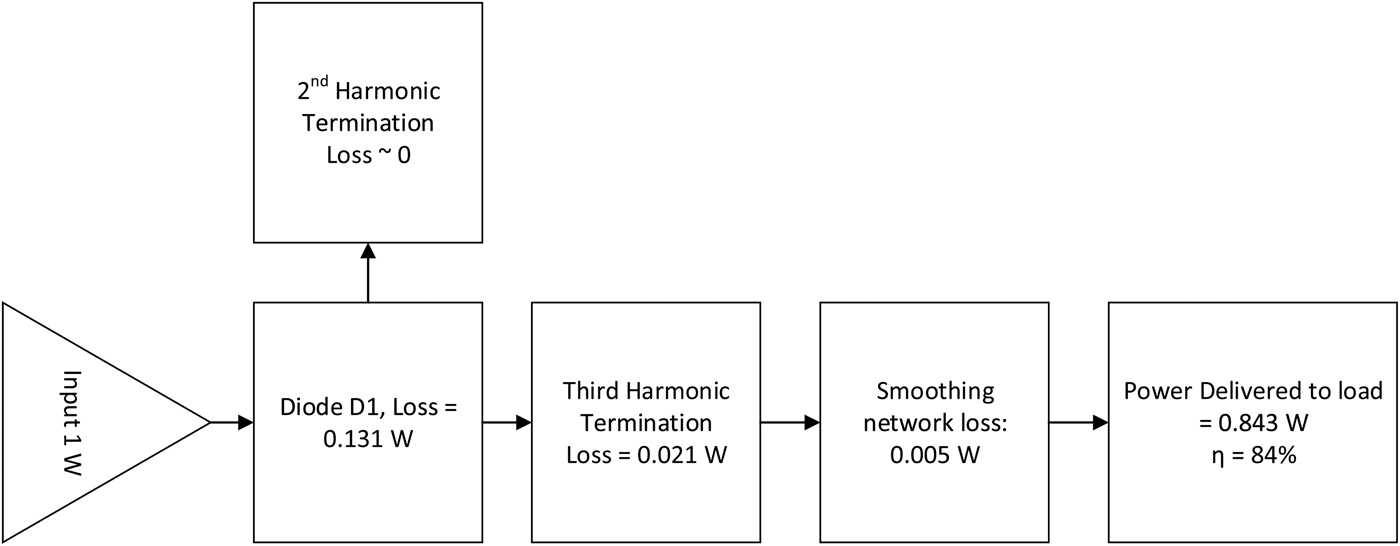
In our design, a maximum efficiency of 84.3% is obtained with a 30 dBm input. Also, for the input power ranging from 28 to 35 dBm, the average conversion efficiency is 80%. Beyond which the diode starts entering the breakdown region. Figure 12 represents the power budget of this design. As explained in the introduction, most losses occur at the diode. However, the deviation in the measured and simulation results are attributed to DCR losses present in the lumped components. Since low frequencies are being used, the dielectric losses in the substrate can be neglected. In this work, either the electrostatic resistance (ESR) or DCR in capacitors and inductors are the main contributors for the loss in rectification efficiency.
Power budget diagram.

There are ways in which the measured results can be improved. First, the efficiency can be brought closer to the simulation results by choosing low tolerance components and components with low parasitic losses. Second, a diode with lower turn ON voltage, lower Rd, and lower junction capacitance [Reference Guo, Zhang and Zhu14] can be chosen.
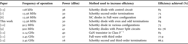
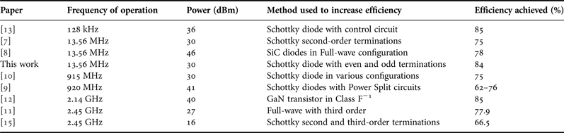
Rectifier designs discussed in literature are listed in Table 2. Kang et al. [Reference Kang, Park, Jang and Lee13] developed a Schottky diode rectifier where a control circuit is used to switch between rectifier and voltage multiplier modes. An impedance matching controller is also implemented to match varying loads. Although a higher conversion efficiency is achieved, a complex architecture is needed. The highest conversion efficiency at 40 dBm is reported by Roberg et al. [Reference Roberg, Reveyrand, Ramos, Falkenstein and Popovic12]. However, this design is implemented using a GaN transistor at a higher frequency with transmission line harmonic terminations. Our design has an advantage over these designs by being simpler to implement and has the highest efficiency at the frequency of operation.
Comparison of rectifier circuits.
IV. CONCLUSION
We have developed a high-efficiency, low-complexity rectifier geared toward short-range wireless power transfer. Such a device will enable fast and efficient charging of devices requiring high power. This will enable wireless charging for not only portable electronic devices, but also for larger devices such as laptops. The flexible design of the rectifier allows it to be customized for use in various wireless power receiver systems.
The rectifier based on a shunt Schottky diode with harmonic terminations is simulated and tested with input power ranging from 27 to 40 dBm. On comparison with similar devices in literature, our design achieves a power efficiency of 84%, which is higher than most shown in Table 2. The highest reported efficiency of 85% in Table 2 comes at the expense of greater design complexity and higher implementation cost than our prototype. Furthermore, the efficiency of our design can readily be improved, if needed, using Schottky diodes with lower junction capacitance and forward voltage, and components with smaller tolerance, ESR and DCR.
ACKNOWLEDGEMENTS
None.
STATEMENT OF INTEREST
None.
 Aasrith Ganti received his B.S. in Electronics and Communication Engineering from the JNT University in 2008 and M.S. in Electrical Engineering in 2014. Presently he is a part of the development team at Philips Healthcare. His main research interests are wireless power transfer, energy harvesting, and semiconductor devices.
 Jenshan Lin received the Ph.D. degree in Electrical Engineering from the University of California at Los Angeles (UCLA), Los Angeles, CA, USA, in 1994. He was with AT&T Bell Laboratories (which later became Lucent Bell Labs), Murray Hill, NJ, USA, from 1994 to 2001, and its spin-off Agere Systems from 2001 to 2003. In July 2003, he joined the University of Florida, Gainesville, FL, USA, as an Associate Professor and became a Professor in August 2007. He has authored or co-authored over 250 technical publications in refereed journals and conferences proceedings, and holds 14 US patents. His research interests include sensors and biomedical applications of microwave and millimeter-wave technologies, wireless power transfer, RF-integrated circuits, and antennas. He is a Fellow of IEEE and currently serves as the Editor-in-Chief of IEEE Transactions on Microwave Theory and Techniques for the term of 2014–2016.
 Raul A. Chinga received his B.S. and Ph.D. degrees from the University of Florida in 2008 and 2013, respectively. His dissertation work concentrated on high efficient power amplifiers for DBD plasma generation for sterilization applications. In addition, he concentrated on wireless power transfer systems via inductive coupling for near field and midrange applications. During his time at the University of Florida, he was awarded the Bridge to the Doctorate Fellowship in 2008, the Graduate Research Fellowship Honorable Mention award by NSF in 2010, and the Varosi Scholarship in 2012. His is currently working at Space Systems Loral in Palo Alto, California, working on various aspects of the spacecraft power system.
 Shuhei Yoshida received his M.S. degree from Keio University, Japan in 2007. His dissertation work concentrated on high efficient wireless power transfer systems and its applications. He is currently working at NEC Corporation in Japan, working on various aspects of the wireless power transfer system.
APPENDIX
Spice model for MBRA140.