Introduction
With the advancement of the wireless communication technology, the demands for bandpass filters (BPFs) with increasingly stringent filtering specifications grow. These BPFs must exhibit low insertion loss, own compact size, be lightweight, offer high selectivity, and possess a wide stopband. Wide stopband BPFs are crucial for effectively mitigating interference signals beyond the passband, which in turn enhances the signal transmission quality and bolsters the overall performance of the communication system. A variety of technologies have been utilized to design the wide-stopband BPFs, including microstrip line (MSL) [Reference Weng, Lan and Chang1–Reference Das, Chatterjee, Rahim and Geok6], substrate integrated waveguide (SIW) [Reference Liu and Cheng7–Reference Azad and Mohan15], and waveguide cavity [Reference Povilas, Kenneth, Rao and Hong16–Reference Abdul and Cristiano18].
Although the MSL and SIW resonators are compact and lightweight, their low-quality factors result in relatively big insertion losses and low selectivity. The waveguide cavity resonators, despite offering low loss and high selectivity, are limited by their metal cavity construction, which leads to large dimensions and heavy weight. Consequently, these traditional resonators are less ideal for the 5G and future communication systems, which demand optimal performance in terms of low loss, compact size, light weight, high selectivity and wide stopband.
Researchers have increasingly focused on dielectric waveguide resonators (DWRs) due to their compelling benefits, such as compact size, low weight and low loss. The BPFs utilizing the DWRs have been extensively documented. In [Reference Huang, Guo, Li, Jiang and Cheng19], isosceles right triangular resonators are integrated into ceramic dielectric waveguides to achieve a reduction in filter dimensions and to minimize interference from higher-order modes. Another research introduces a novel and tunable DWR featuring a distinctive design [Reference Qin, Liu, Yang, Chen, Li and Xu20]. The non-metalized blind holes on the dielectric’s top surface, in conjunction with tuning screws on the Printed Circuit Board (PCB), allow for adjustable and reversible resonant frequency tuning. The study in [Reference Lu, Zhou, Qin, Yang and Chen21] presents a traditional rectangular DWR with orthogonal ridges on both the upper and lower surfaces. This design, when compared to the traditional dual-parallel-ridged DWRs, features a smaller size, a higher quality factor, and more effective suppression of harmonic frequencies. In [Reference Xie, Chen and Chu22] and [Reference Huang, Cheng and Zhang23], DWRs based on dual-mode resonators are proposed, which can achieve flexible control of transmission zeros through adjusting the positions of blind holes. Although the above DWRs exhibit superior performance, they still cannot achieve wide stopband suppression.
The application of hybrid resonator technology has emerged as a focal point in microwave communication research. This approach utilizes a variety of resonators to enhance the filter performance, aligning with different performance requirements for the BPFs in modern wireless communication systems. It describes a design in [Reference Jiao, Zhu, Chu, Yu and Luo24] where an MSL resonator is sandwiched between two SIW cavities, which effectively increases the filter’s order without extra space, thus facilitating miniaturization. In [Reference Zheng, Zhu, Wang and Dong25], a high-selectivity hybrid BPF is proposed for the K-band, utilizing an inverted microstrip gap waveguide technique. This design integrates slot-gap waveguide cavity resonators with microstrip stub-loaded ring resonators, showcasing superior selectivity. In [Reference Zheng and Dong26], a shielded quarter-mode SIW combined with microstrip technology is employed to achieve significant stopband attenuation, which shows the possibility of designing wide stopband BPFs by utilizing distinct resonators. Therefore, it is meaningful and practical to propose different kinds of DWRs and design wide-stopband BPFs for the 5G and future wireless communication systems.
In this study, three distinct types of DWRs will be proposed by incorporating metallized blind holes, metallized U-shaped slots, and parallel ridges into the conventional rectangular DWRs. These resonators are designed in purpose to maintain the same external dimensions and fundamental mode frequencies, yet their harmonic frequencies are staggered. Furthermore, using different structures for adjacent resonators helps to prevent the coupling of higher-order modes that typically occurs between identical resonators, thus effectively reducing the emergence of undesired harmonic passbands. For the purposed of verification, a sixth-order BPF will be designed and characterized by using the proposed three kinds of DWRs. The measured results show accordance with the simulated ones. The 20 dB stopband attenuation reaches up to 2f 0, where f 0 representing the center frequency of the passband. The minimum in-band insertion loss is about 1 dB. These attributes make the proposed BPF a promising candidate for the applications in modern communication systems where wide stopband and low insertion loss are essential.
Analysis of the distinct DWRs
Based on the conventional rectangular DWR, three distinct DWRs are developed. As depicted in Fig. 1(a) and (c), the modifications involve etching a metallized blind hole and a metallized U-shaped slot at the center of the DWR’s top surface. They are marked as Resonator A and Resonator B in the following parts, respectively. The radius and height of the blind hole are denoted by ra and ha, respectively. The width and height of the U-shaped slot are represented by wm and hm. Figure 1(e) illustrates the introduction of a pair of parallel ridge structures within the DWR, with one ridge positioned at the center of the top surface and the other at the center of the bottom surface. It is named as Resonator C. The dimensions of the ridges are characterized by their width wu and height hu. Each resonator maintains identical external dimensions, with l, w, and h signifying the length, width, and height. The ceramic material used owns a relative permittivity εr of 20.3 and a loss tangent of 0.00015. The external surfaces of all resonators are metallized by using a standard silver-plating technique, resulting in a final plating thickness of approximately 20 µm.
3D structures of the three DWRs and the electric field distributions of their corresponding TM110 mode: (a) structure and (b) field of the DWR with metalized blind hole (Resonator A); (c) structure and (d) field of the DWR with metalized U-shaped slot (Resonator B); (e) structure and (f) field of the DWR with dual parallel ridges (Resonator C).

According to the electric field distributions in Fig. 1, the fundamental modes of the three DWRs are generally the TM110 mode. In Fig. 1(b), the introduction of a blind hole into the structure disrupts the electric field distribution, leading to a concentration of the field near the hole. In Fig. 1(d), we proposed a novel DWR with metalized U-shaped slot. The two ends of the U-shaped slot are strategically positioned in regions where the electric field of the higher-order mode is relatively strong. This placement significantly increases the slot’s influence on the higher-order mode resonance frequencies. As a result, the separation of harmonics among the three resonators used in this design is effectively enhanced. In Fig. 1(f), the electric field is compressed between the two parallel ridges, as the ridges’ presence increases capacitance in these regions, drawing the field lines toward the ridges. Consequently, the electric field strength is elevated in areas adjacent to the ridges.
Since the three distinct DWRs will be used for the BPF designs, it is essential to thoroughly investigate their fundamental modes in terms of the resonant frequency (fr) and the unloaded quality factor (Qu). As depicted in Fig. 2, the frs and the Qus of their fundamental modes vary with different physical parameters, where ra and ha represent the radius and height of the metalized blind hole, wm and hm are the width and height of the metallized U-shaped slot, and wu and hu are the width and height of the ridges. It can be seen from Fig. 2(a) and (b) that fr of Resonator A declines as ra and ha increases, fr of Resonator B decreases with the increase in wm and hm, and fr of Resonator C is also found to decrease when wu and hu increases. Importantly, for all the three DWRs, fr can be easily adjusted to the same frequency, e.g., 3.45 GHz. Although the Qu of Resonator C is comparatively lower than those of the other two DWRs, as illustrated in Fig. 2(c) and (d), the Qus of all the three types of DWRs are within the same order of magnitude, which is important to design BPFs constructed by coupled resonators.
The effects of physical parameters on frs and Qus of the fundamental modes of the three DWRs: (a) fr versus 2ra, 2wm, or wu; (b) fr versus ha, hm, or hu; (c) Qu versus 2ra, 2wm, or wu; and (d) Qu versus ha, hm, or hu.

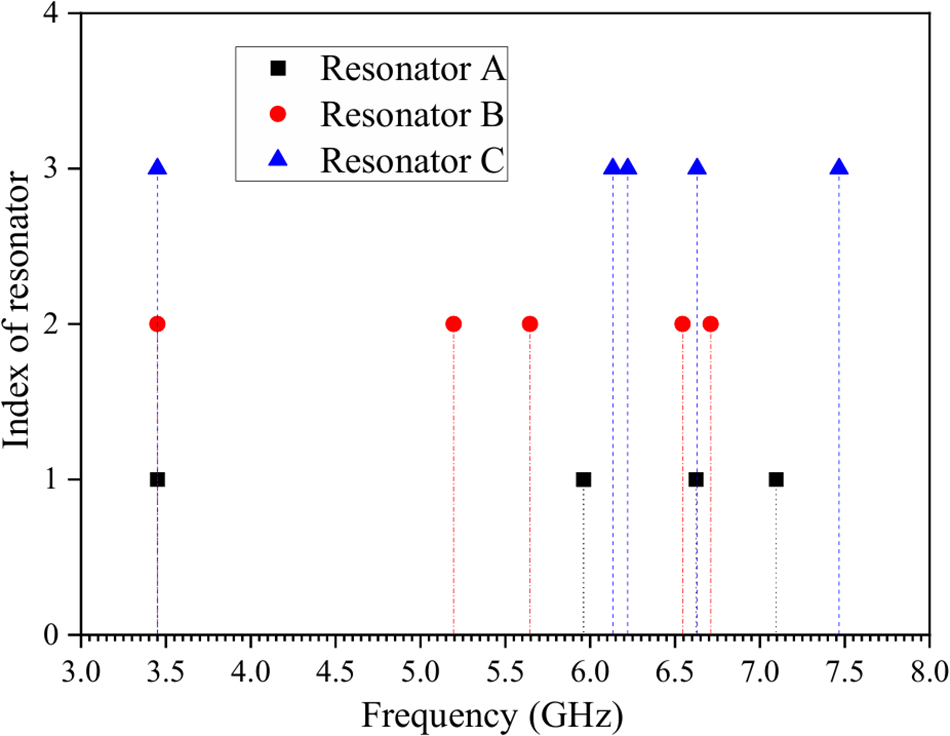
To precisely set the fundamental frequencies of the three DWRs to 3.45 GHz, the physical parameters illustrated in Fig. 2 have been carefully selected (unit: mm): w = l = 11.1, h = 5.8, ra = 2.35, ha = 1.9, wm = 1.85, hm = 1.95, wu = 3, hu = 2.25. Under these specified dimensions, the simulated frequencies for the first five modes of the three DWRs are presented in Table 1. Figure 3 provides a visual representation of the distribution of these modes. It is observed that the fundamental frequencies of the resonators are the same, while their higher-order harmonics are sequentially offset. Although Table 1 may suggest that the combination of Resonators A and B can achieve good out-of-band performance, when the same resonator A is used at both the input and output, the identical resonators B will be adjacent to each other, thereby introducing additional harmonics and degrading the out-of-band performance. To avoid this situation, a new resonator C needs to be introduced. Notably, the fourth harmonics of Resonators A and C are almost coincident at a frequency of approximately 6.62 GHz, which is supposed to result in the nearest spurious response within the upper stopband. Fortunately, Resonator B does not exhibit a resonance at 6.62 GHz. Therefore, the spurious response at 6.62 GHz would be mitigated to a certain degree if the three DWRs are employed in the design of BPFs.
Frequency distributions for the first five modes of the three DWRs.

Resonant frequencies of the first five modes for the three DWRs

DWR BPF using hybrid resonators
In this section, the design of a sixth-order BPF utilizing the three distinct types of DWRs is presented. The primary objective is to demonstrate the effectiveness of this technique in achieving significant harmonic suppression. As shown in Fig. 4, its structure primarily consists of two parts: the dielectric part and the PCB part. The ceramic dielectric section is mounted and electrically connected to the PCB. The dielectric part of the proposed filter is molded by the dielectric powders, which is mainly composed of MgTiO3 and CaTiO3. The molded dielectric body is baked to be fixed. The outer surfaces of the dielectric body are metallized by silver spraying process. Laser etching process is utilized to remove the silver to form the unmetallized ring. The PCB part is fabricated on a Rogers 4003C PCB substrate, characterized by a relative permittivity of 3.55 and a thickness of 0.813 mm. Figure 5 illustrates the coupling mechanism, the couplings between adjacent resonators are realized by the coupling windows.
Structure of the proposed DWR BPF. (Key physical parameters (unit: mm) are w = l = 11.1, h = 5.8, L1 = 5.85, L2 = 5.6, L3 = 5.45, W1 = 1.35, W2 = 1.45, W3 = 1.2, hkd = 0.9, wp = 28.1, lp = 90.1, hp = 0.813, and lf = 13.).

Coupling topology of the proposed DWR BPF.

The objective BPF is characterized by the following key specifications: a center frequency f0 of 3.45 GHz, an operational bandwidth ranging from 3.4 to 3.5 GHz, a fractional bandwidth (FBW) of approximately 2.9%, an in-band return loss better than 20 dB. Based on these specifications, the normalized coupling matrix can be synthesized by employing the traditional coupled resonator theory as
 \begin{equation}\left[ M \right] = \left[ {\begin{array}{*{20}{c}}
0&{{\text{0}}{\text{.999}}}&0&0&0&0&0&{\text{0}} \cr
{{\text{0}}{\text{.999}}}&{\text{0}}&{{\text{0}}{\text{.822}}}&0&0&0&0&0 \cr
0&{{\text{0}}{\text{.822}}}&0&{{\text{0}}{\text{.61}}}&0&0&0&0 \cr
0&0&{{\text{0}}{\text{.61}}}&0&{{\text{0}}{\text{.566}}}&0&0&0 \cr
0&0&0&{{\text{0}}{\text{.566}}}&{\text{0}}&{{\text{0}}{\text{.587}}}&0&0 \cr
0&0&0&0&{{\text{0}}{\text{.587}}}&{\text{0}}&{{\text{0}}{\text{.833}}}&0 \cr
0&0&0&0&0&{{\text{0}}{\text{.833}}}&0&{{\text{0}}{\text{.999}}} \cr
{\text{0}}&0&0&0&0&0&{{\text{0}}{\text{.999}}}&0
\end{array}} \right].\end{equation}
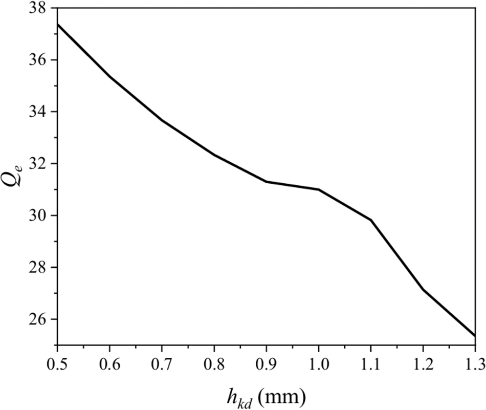
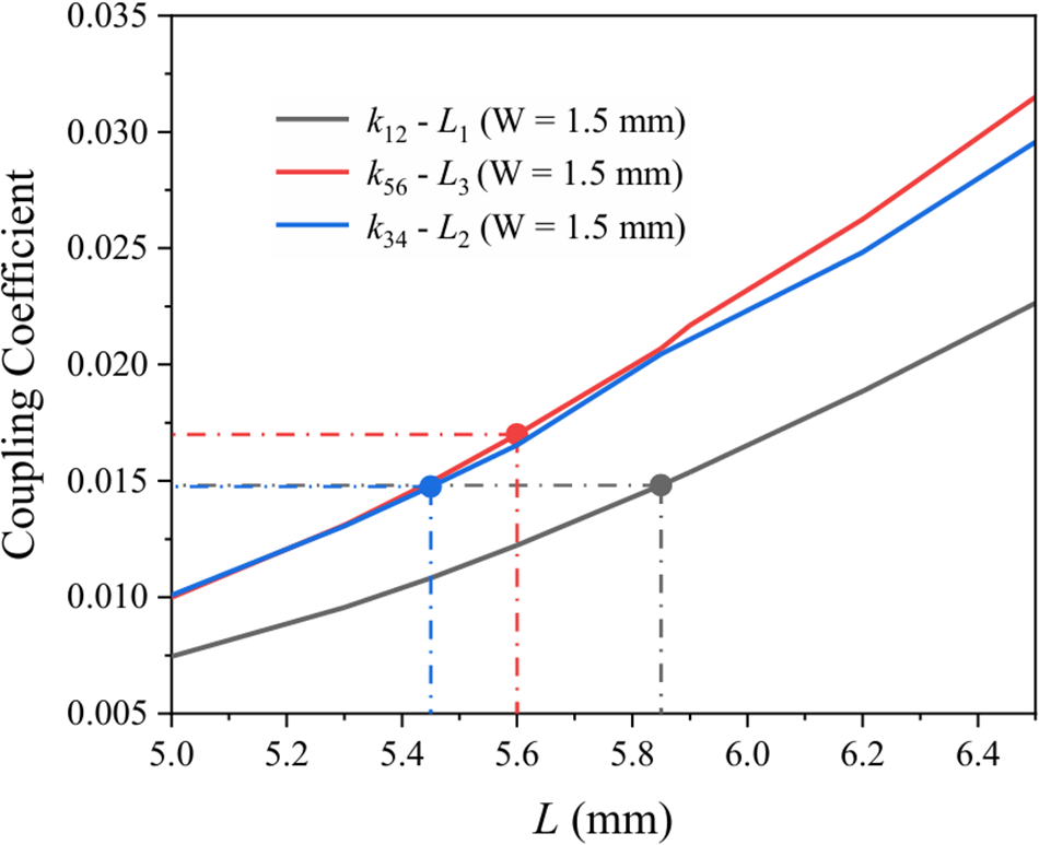
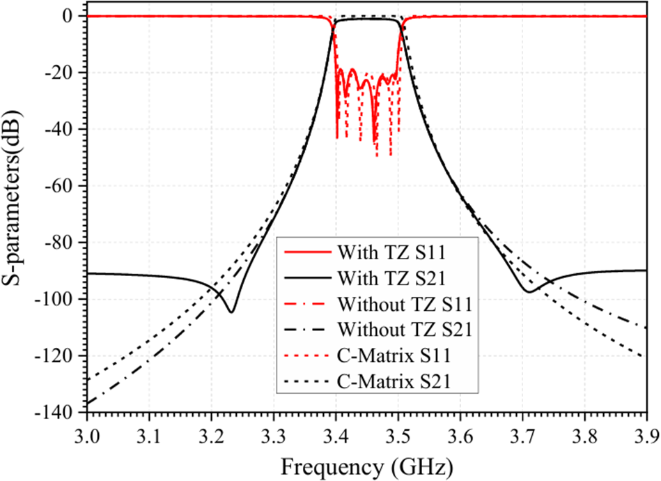
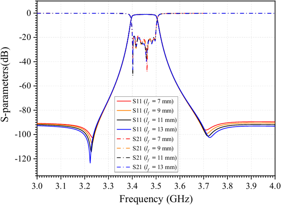
Simulations are conducted to determine the external quality factor (Qe) and the actual coupling coefficient (k). Figure 6 demonstrates the influence of the height of the feeding blind hole (hkd) on the Qe, whereas Fig. 7 highlights the effect of the coupling window length (L) on k. According to the derived values of k and Qe, a sixth-order DWR BPF was designed and simulated. The simulated performance within the 3-4 GHz frequency range is depicted by the solid lines in Fig. 9. It is noteworthy that the filter exhibits two transmission zeros (TZs) at 3.232 and 3.713 GHz on lower and upper sides of the passband, respectively. However, these TZs were not anticipated based on the initial filter design and the proposed coupling topology. The reason is that the PCB feed structure introduces a weak electric coupling between the input and output ports, resulting in the emergence of these TZs. To substantiate this hypothesis, the input and output ports were isolated by a metal block in the simulation model, as shown in Fig. 8. The rectangular metal block is placed at the center of the PCB, separating the two sides of the air box. In this case, there is no coupling between Port 1 (S) and Port 2 (L), and the simulation results within the passband show no significant difference compared to when the metal isolation block is not placed. The dashed lines in Fig. 9 present the corresponding results, which confirm the disappearance of the TZs. Since the TZs originate from the PCB rather than the dielectric component, they could be independently adjustable. By modifying the length lf of the feeding MSL as indicated in Fig. 4, the position of the TZs can be manipulated. Figure 10 illustrates that as lf increases, the TZs move further away from the passband, while the passband almost remains constant. Consequently, the coupling topology and the normalized coupling matrix of the filter require refinement, as displayed in Fig. 11 and Matrix (2).
 \begin{equation}\left[ M \right] = \left[ {\begin{array}{*{20}{c}}
0&{{\text{0}}{\text{.999}}}&0&0&0&0&0&{{\text{ - 0}}{\text{.00018}}} \cr
{{\text{0}}{\text{.999}}}&{\text{0}}&{{\text{0}}{\text{.822}}}&0&0&0&0&0 \cr
0&{{\text{0}}{\text{.822}}}&0&{{\text{0}}{\text{.61}}}&0&0&0&0 \cr
0&0&{{\text{0}}{\text{.61}}}&0&{{\text{0}}{\text{.566}}}&0&0&0 \cr
0&0&0&{{\text{0}}{\text{.566}}}&{\text{0}}&{{\text{0}}{\text{.587}}}&0&0 \cr
0&0&0&0&{{\text{0}}{\text{.587}}}&{\text{0}}&{{\text{0}}{\text{.833}}}&0 \cr
0&0&0&0&0&{{\text{0}}{\text{.833}}}&0&{{\text{0}}{\text{.999}}} \cr
{{\text{ - 0}}{\text{.00018}}}&0&0&0&0&0&{{\text{0}}{\text{.999}}}&0
\end{array}} \right]\end{equation}
Extracted Qe versus hkd.

Extracted coupling coefficients k 12, k 34, and k 56 versus L 1, L 2, and L 3, respectively.

Simulation results and structure of the proposed DWR BPF without TZs.

Simulation and coupling matrix results of S-parameters.

The influence of feeding microstrip line length lf on TZs.

The improved coupling topology of the proposed DWR BPF.

Figure 12 shows photographs of the fabricated dielectric part and the assembled BPF. The dimensions of the dielectric part are 73 mm × 11.1 mm × 5.8 mm, which correspond to 3.78λg × 0.54λg × 0.32λg (λg is the guided wavelength at the center frequency f 0 = 3.45 GHz). The assembled BPF was measured by using the Agilent N5230C vector network analyzer. The comparison between the simulated and measured results is presented in Fig. 13. During the integral manufacturing process, the dielectric part experiences high-temperature firing and cooling, which induces volumetric contraction. To counteract this, the part is initially oversized based on the anticipated shrinkage rate, resulting in an initial volume that exceeds the design and simulation models. Ideally, the final dimensions should closely align with the simulated ones to ensure accurate results. For conventional components such as coupling windows, blind holes, and ridges, shrinkage rates are well-characterized and reliably controlled. However, the U-shaped slot resonator presents a unique challenge due to the lack of experience in describing and measuring its cooling-induced dimensional deviations. This uncertainty leads to a significant discrepancy (approximately 8 dB) between the measured and simulated return losses, emphasizing the need for further empirical research and process refinement to enhance dimensional accuracy. As an important indicator of filter performance, insertion loss affects system efficiency. In Fig. 14, the effects of different conductivity σ, conductor surface roughness Rq and dielectric loss tangent tan δ on the insertion loss of the filter are given. With the increase of σ, the insertion loss decreases. On the contrary, when Rq and tan δ increase, the insertion loss increases. Notably, no TZs are detected in the measurement. This absence is attributed to the fact that the S-parameters measurement range of the vector network analyzer used in our laboratory is limited; the position where the zero point appears is buried in the noise floor. The proposed filter operates in the frequency band from 3.4 to 3.5 GHz. It achieves a minimum in-band insertion loss of approximately 1.0 dB, with a return loss better than 12 dB. The stopband suppression, which is greater than 20 dB, extends from 3.47 to 6.9 GHz, reaching up to twice the center frequency 2f 0.
Photographs of the fabricated DWR BPF: (a) top of the dielectric part, (b) bottom of the dielectric part, (c) top view of the assembled BPF, (d) bottom view of the assembled BPF, and (e) side view of the assembled BPF.

Simulated and measured results of the proposed DWR BPF: (a) narrow-band view and (b) wideband view.

The influence of different parameter variables on the filter insertion loss: (a) conductivity σ; (b) surface roughness Rq; (c) loss tangent tan δ.

Table 2 presents a comparative analysis of the proposed BPF with previously reported BPFs. The proposed filter showcases a broader stopband suppression compared to the precious designs. Furthermore, as compared with the BPFs by combining SIW and MSL resonators in [Reference Jiao, Zhu, Chu, Yu and Luo24–Reference Zheng and Dong26], the proposed one features lower insertion loss. Although its insertion loss is similar to that of the BPF in [Reference Jiao, Zhu, Chu, Yu and Luo24], it is a sixth-order filter, whereas the one in [Reference Jiao, Zhu, Chu, Yu and Luo24] is a third-order BPF. To be concluded, the proposed BPF stands out with low loss, compact size, light weight, and extended stopband.
Comparisons with previous prototypes

RL: return loss, FS: frequency shift, IL: insertion loss, FO: filter order, SB: stopband of 20-dB rejection.
Conclusion
This paper introduces a novel approach to realizing wide stopband BPFs by investigating the harmonic characteristics of three distinct types of DWRs. A new DWR featuring a metallized U-shaped slot is proposed. This design effectively enhances the separation of harmonic frequencies while maintaining consistent fundamental frequencies. Additionally, the arrangement of the resonators is meticulously planned, with adjacent resonators being of different types. This configuration prevents coupling between higher-order modes of the same type, thereby further suppressing the generation of undesired harmonic passbands and achieving effective harmonic suppression. To substantiate the practicality of this technique, a sixth-order wide stopband DWR BPF was designed and measures, utilizing the investigated three distinct DWRs. The measured results are in close concordance with the simulated ones. It was found that the proposed BPF features low loss, compact size, light weight and wide stopband simultaneously, making it applicable to the base station of the 5G and future wireless communication systems.
Funding statement
This work was supported by the National Natural Science Foundation of China under grants 62371260 and 61971244.
Competing interests
The authors report no conflict of interest.

Ke-Lan Li was born in Xuzhou, Jiangsu Province, China, in 1999. He received the B.S. degree from Nantong University, Nantong, Jiangsu Province, China, in 2022. He is currently pursuing the M.S. degree in electromagnetic field and microwave technology at Nantong University, Nantong, Jiangsu Province, China. His research interest is in wide stopband dielectric waveguide filter circuits.

Wei Huang was born in Zhenjiang, Jiangsu Province, China, in 2000. He received the B.S. degree from Nantong University, Nantong, in 2022. He is currently pursuing the M.S. degree in electromagnetic field and microwave technology in Nantong University, Nantong, China. His current research interest is multimode dielectric waveguide filter.

Wei Qin was born in Nantong, Jiangsu, China, in 1984. He received the B.Sc. degree in electronic engineering and the M.Sc. degree in electromagnetic fields and microwave technology from Southeast University, Nanjing, China, in 2007 and 2010, respectively, and the PhD degree in electronic engineering from City University of Hong Kong, Hong Kong, China, in 2013. From July 2013 to November 2013, he was a senior research associate with the State Key Laboratory of Millimeter Waves (HK), City University of Hong Kong, Hong Kong, China. Since 2014, he has been with Nantong University, Nantong, China, where he is currently a Professor. His research interest focuses on deign and application of microwave devices and antennas.

Jian-Xin Chen was born in Nantong, Jiangsu Province, China, in 1979. He received the B.S. degree from Huai Yin Teachers College, Jiangsu Province, China, in 2001, the M.S. degree from the University of Electronic Science and Technology of China (UESTC), Chengdu, China, in 2004, and the Ph.D. degree from the City University of Hong Kong, Kowloon, Hong Kong, in 2008. Since 2009, he has been with Nantong University, Jiangsu Province, China, where he is currently a Professor. He has authored or coauthored more than 100 internationally referred journal and conference papers. He holds 25 Chinese patents and 3 U.S. patents. His research interests include microwave active/passive circuits and antennas, LTCC-based microwave and millimeter-wave filters and devices, and dielectric resonator (DR) filters and antennas.