Multiferroic magnetoelectric nanostructures
Many of today’s technological challenges require integration of two or more monolithic material components. Much attention has therefore been paid to the study of interfacial coupling between individual components in composite material systems, Reference Yang and Tarascon1,Reference Hwang, Iwasa, Kawasaki, Keimer, Nagaosa and Tokura2 where new functionalities can arise from coupling among different variables (order parameters) across the interfaces (see the Introductory article in this issue). In particular, in composite nanostructures with relatively large numbers of interfaces, one can utilize these new functionalities to achieve ultimate performance in a device.
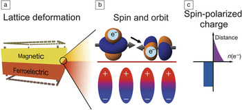
One good example is multiferroic magnetoelectric nanostructures, with magnetic and ferroelectric materials integrated at the nanoscale. Figure 1 shows a nanostructure with juxtaposed magnetic and ferroelectric layers. Across the interface, electric polarization in the ferroelectric layer can be coupled to the magnetization in the magnet, based on the interplay among the lattice, charge, spin, and orbit degrees of freedom achieved typically through the exchange of certain type(s) of potential energy, such as mechanical, electric, and magnetic. Such coupled polarization and magnetization further enable an electrically tunable magnetization or a magnetically tunable polarization, known as converse and direct magnetoelectric coupling, respectively. In this article, we review several novel device prototypes based on interface-based magnetoelectric coupling and provide a brief outlook. Details of recent progress in multiferroic magnetoelectric nanostructures can be found in existing review articles (e.g., References Reference Ma, Hu, Li and Nan3–Reference Fusil, Garcia, Barthélémy and Bibes6).
Interplay among lattice, spin, orbit, and charge degrees of freedom across a magnetic–ferroelectric interface induces coupled magnetization and electric polarization. (a) Lattice deformation (strain) can act over a long spatial scale. (b) Polarization charges in the ferroelectric region can attract or repel spin-polarized electrons in the interface region of the magnet, as schematically shown in (c) by the density of spin-polarized electrons, n(e–), in the case where electrons are attracted to the interface. Accordingly, interfacial magnetism can be modulated based on electrically induced changes in interfacial spin polarization and interfacial orbital configuration.

Ultrahigh-density magnetic memories
Based on converse magnetoelectric coupling in multiferroic magnetoelectric nanostructures, the magnetization is switched with an electric field (via, strain Reference Eerenstein, Wiora, Prieto, Scott and Mathur7–Reference Lahtinen, Franke and van Dijken12 or exchange bias Reference Chu, Martin, Holcomb, Gajek, Han, He, Balke, Yang, Lee, Hu, Zhan, Yang, Fraile-Rodriguez, Scholl, Wang and Ramesh13–Reference Heron, Bosse, He, Gao, Trassin, Ye, Clarkson, Wang, Liu, Salahuddin, Ralph, Schlom, Iniguez, Huey and Ramesh18 across the interface) rather than a current. This property can be exploited to lift the obstacles now limiting the storage densities of magnetic memories.
Ultrahigh-density hard disk drive
The density limit for a hard disk drive (HDD) is set by the thermal stability of one storage unit that consists of a number of magnetic grains (typically 50–100) in a granular recording medium. Reference Richter19 This density limit is about 1 Tb in–2 for state-of-the-art perpendicular recording technology, where the bit information (i.e., 0 and 1) is represented by the polarity of a magnetization aligning perpendicularly to the plane of the recording medium. 20 To achieve higher area density, the thermal stability of one storage unit, expressed as K u V m/k B T (where K u is the uniaxial magnetic anisotropy energy potential, V m is the effective volume of the storage unit that contributes to magnetic energy, k B is the Boltzmann constant, and T is the temperature in Kelvin), must be enhanced. Reference Richter19
The first approach to enhancing thermal stability is by utilizing perpendicular recording media with higher K u values. However, the magnetic coercive field (H c) would also become higher and eventually go beyond the available write magnetic field. Write assist is therefore required to reduce H c momentarily. For example, an electric field can be utilized to assist magnetization reversal (i.e., electrically assisted magnetic recording [EAMR]) Reference Zavaliche, Zhao, Zheng, Straub, Cruz, Yang, Hao and Ramesh8,Reference Zhou, Liu, Zhang and Schreck21 by reducing H c in a single magnetic thin film Reference Zhou, Leong, Yuan, Hu, Ong and Liu22 or, more efficiently, in a recording medium based on multiferroic magnetoelectric nanostructures. Reference Zavaliche, Zhao, Zheng, Straub, Cruz, Yang, Hao and Ramesh8 In these nanostructures, marked reductions of H c have been observed Reference Ma, Hu, Li and Nan3,Reference Wang, Ma, Li, Shen, Lin and Nan23 during electrically driven magnetization switching due to the associated large change in magnetic anisotropy. In particular, a strain-mediated, electrically driven reduction in perpendicular magnetic anisotropy (and/or H c) has recently been observed in an L10-ordered (a type of face-centered cubic-based-ordered structure) FePt film, Reference Tsai, Liao, Huang, Wang and Lai24 one of the promising candidates for practical perpendicular recording media, Reference Thiele, Maat and Fullerton25 and in an ultrathin (1.1-nm-thick) Co20Fe60B20 film; Reference Yu, Wang, Abolfath-Beygi, He, Li, Wong, Nordeen, Wu, Carman, Han, Alhomoudi, Amiri and Wang26 both are grown on top of a Pb(Mg1/3Nb2/3)0.7Ti0.3O3 (PMN-PT) substrate.
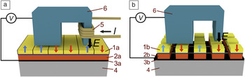
Compared to another emerging technology of heat-assisted magnetic recording (HAMR) Reference Rottmayer, Batra, Buechel, Challener, Hohlfeld, Kubota, Li, Bin, Mihalcea, Mountfield, Pelhos, Peng, Rausch, Seigler, Weller and Yang27,Reference Kryder, Gage, McDaniel, Challener, Rottmayer, Ganping, Hsia and Erden28 that involves the use of heat from a focused laser beam to reduce H c, EAMR is much easier to achieve, as it does not require the complex integration of optical, electronic, and magnetic device components in write heads, and therefore can potentially lead to higher storage densities. Figure 2a schematically shows one possible setup of EAMR, where a horizontal multiferroic magnetoelectric nanostructure (i.e., juxtaposed nanometer-thick magnetic and ferroelectric films) is considered as the recording medium.
Schematics of (a) electrically assisted magnetic recording, where an electric field (E) is generated across the storage unit by applying a voltage (V) through the write head and an electrode layer underneath the ferroelectric layer. (b) Possible electrically driven magnetic recording under zero magnetic field in high-density arrays of magnetic–ferroelectric nanoislands, namely, bit-patterned magnetoelectric media, where the electric field is selectively applied across the isolated storage unit through the write head and the patterned bottom electrode. Perpendicularly magnetized recording media are considered in all cases, with the arrows indicating magnetization orientations. For simplicity, only the principle of the writing process is shown. (a) Prepared on the basis of Reference 21. Magnetic and ferroelectric thin films in (a) (1a and 2a, respectively) and nanoislands (1b and 2b, respectively) in 2b; (3a) thin-film and (3b) patterned electrode underlayer in 2a and 2b, respectively; (4) substrate; (5) write coil; and (6) Yoke/return pole. Note: I, current.

The second approach to enhancing thermal stability is to increase the effective volume of a storage unit (i.e., V m). For example, it is possible to replace the continuous magnetoelectric composite thin films in Figure 2a with high-density bit-patterned arrays of isolated multiferroic magnetoelectric nanoislands, or bit-patterned magnetoelectric media (BPMeM), as shown in Figure 2b. In this case, each magnetic island represents one storage unit, and the entire volume of the island (V i) can contribute to the magnetic anisotropy energy (i.e., V m = V i). More promisingly, purely electric-field-driven 90° and 180° perpendicular magnetization switching have recently been computationally demonstrated in BPMeM using phase-field simulations, Reference Hu, Yang, Chen and Nan29,Reference Hu, Yang, Wang, Huang, Zhang, Chen and Nan30 indicating the possibility of achieving electrically driven magnetic recording (EDMR) under zero magnetic fields (hence without requiring the write coil; see Figure 2b). This EDMR technology can enable ultrahigh-density HDD benefiting from both the much simpler structure and the much lower heat dissipation requirement. (Ideally, there should be no leakage current during writing.)
Ultrahigh-density magnetic random-access memory
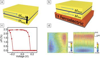
Magnetic random-access memory (MRAM) is one of the most promising types of “universal memory” Reference Åkerman31,Reference Zhu32 that has the potential to replace static random-access memory (SRAM) as the cache memory of the central processing unit, dynamic random-access memory (DRAM) as the principal working memory, or flash memory for permanent data storage. In state-of-the-art MRAM, magnetization in one of the two magnetic layers (separated by a nonmagnetic layer; see Figure 3a) is switched by 180° with a current (I) through spin-transfer torque, Reference Slonczewski33,Reference Berger34 inducing high and low electrical resistance states for antiparallel and parallel magnetization alignment through giant magnetoresistance Reference Baibich, Broto, Fert, Van Dau, Petroff, Etienne, Creuzet, Friederich and Chazelas35,Reference Binasch, Grünberg, Saurenbach and Zinn36 or tunnel magnetoresistance. Reference Julliere37,Reference Moodera, Kinder, Wong and Meservey38 However, the heat dissipation from the current limits the storage density. Thus, a significant amount of research effort has recently been devoted to reducing the threshold current of triggering magnetization reversal Reference Brataas, Kent and Ohno39 by utilizing, for example, vertical current injection Reference Khvalkovskiy, Zvezdin, Gorbunov, Cros, Grollier, Fert and Zvezdin40–Reference Metaxas, Sampaio, Chanthbouala, Matsumoto, Anane, Fert, Zvezdin, Yakushiji, Kubota, Fukushima, Yuasa, Nishimura, Nagamine, Maehara, Tsunekawa, Cros and Grollier42 or an assisting electric field. Reference Wang, Li, Hageman and Chien43
Schematics of (a) a trilayered magnetoresistive element consisting of two magnetic layers (yellow) separated by a nonmagnetic metallic spacer or dielectric tunnel barrier (blue) in magnetic random-access memory (MRAM), where the reversal of magnetization (M free) in the free layer (top) can be driven by a spin-polarized current (I), leading to parallel or antiparallel magnetic alignment between M free and magnetization with a fixed direction (M fixed) in the bottom magnetic layer. (b) A trilayered magnetoresistive element on top of a ferroelectric layer with a bottom electrode for magnetoelectric RAM applications. An electric field (E) applied across the ferroelectric layer can switch the magnetization in its adjacent free layer (M free) by 90° and even 180° according to recent reports (see text). (c) Electrically driven nonvolatile electric resistance switching in a magnetoresistive element consisting of a nickel-free layer and a 2-μm-thick (011) Pb(Mg1/3Nb2/3)0.7Ti0.3O3 ferroelectric layer (ΔR, change in electrical resistance). (d) In-plane magnetization vector distributions in the nickel corresponding to the high- (left) and low- (right) resistance states under zero voltages. m z indicates the out-of-plane component of the normalized magnetization. (c) Adapted from Reference 45. (d) Reproduced with permission from Reference 45. © 2011 Nature Publishing Group.

In parallel, switching magnetization with an electric field, because of its negligible heat dissipation, can be exploited for the design of ultrahigh-density MRAM [i.e., magnetoelectric RAM (MeRAM)]. Reference Wang, Alzate and Amiri44 For example, using phase-field simulations, a multiferroic magnetoelectric-nanostructure-based MeRAM with an area density of up to 88 Gb in–2 was computationally demonstrated. Reference Hu, Li, Chen and Nan45 The core unit of such an MeRAM is shown in Figure 3b. During writing, an electric voltage is applied perpendicularly across the nanostructure of a magnetic free layer on top of a ferroelectric layer, and the switching of magnetization in the free layer (M free) is then triggered based on magnetoelectric coupling across the interface. The heat dissipation during this process would be negligible if the ferroelectric were sufficiently insulating. The energy consumption can be estimated as 0.5CV Reference Hwang, Iwasa, Kawasaki, Keimer, Nagaosa and Tokura2 (where C is the capacitance and V is the driving voltage), that is, the energy required to charge a capacitor. If perfect surface screening of polarization charges in the ferroelectric capacitor is assumed, the energy consumption can be further approximated as 0.5P r SV (where P r is the remnant polarization, and S is the electrode area, which equals the in-plane size of the magnetic free layer according to Figure 3b).
Taking a juxtaposed 64 nm × 64 nm × 5 nm nickel nanomagnet and a PMN-PT ferroelectric layer as a representative nanostructure, the simulated loop of the change in electrical resistance of the entire magnetoresistive multilayer (ΔR) versus the driving voltage (V) is shown in Figure 3c. The distinct electric resistance states (ΔR ≈ 2.5%) at V = 0 are induced by the nonvolatile (i.e., stable in the absence of the driving voltage) almost 90° magnetization switching in the nickel free layer (see Figure 3d), mediated by nonvolatile piezostrains from PMN-PT. Reference Wu, Bur, Zhao, Mohanchandra, Wong, Wang, Lynch and Carman46
An ultralow energy consumption as low as 0.16 fJ is then estimated, which is almost three orders of magnitude smaller than that of MRAM (∼0.1 pJ Reference Ohno47 ). The low magnitude of the driving voltage (i.e., ∼0.26 V) is also compatible with complementary metal oxide semiconductor (CMOS) platforms. Recent progress in fabricating high-quality PMN-PT thin films of giant piezoelectric response on a silicon substrate Reference Baek, Park, Kim, Aksyuk, Das, Bu, Felker, Lettieri, Vaithyanathan, Bharadwaja, Bassiri-Gharb, Chen, Sun, Folkman, Jang, Kreft, Streiffer, Ramesh, Pan, Trolier-McKinstry, Schlom, Rzchowski, Blick and Eom48 provides a solid basis for the experimental demonstration of such an MeRAM device prototype.
Furthermore, strain-mediated electrically driven full 180° magnetization switching has recently been proposed for horizontal multiferroic magnetoelectric nanostructures. Reference Hu, Yang, Wang, Huang, Zhang, Chen and Nan30,Reference Wang, Hu, Ma, Zhang, Chen and Nan49–Reference Roy, Bandyopadhyay and Atulasimha51 On one hand, this full magnetization switching would enhance the magnitude of the electric resistance change of the magnetoresistive multilayer to achieve a higher signal-to-noise ratio. On the other hand, it would significantly enhance the reliability of the proposed MeRAM, because the proposed 180° magnetization switching takes place between the two degenerate directions of one built-in magnetic easy axis in the nanomagnet. In this case, the switched magnetization would remain stable even when the piezostrains were completely relaxed.
The proposed MeRAM concept has also been demonstrated in a BiFeO3-based multiferroic magnetoelectric nanostructure, Reference Heron, Bosse, He, Gao, Trassin, Ye, Clarkson, Wang, Liu, Salahuddin, Ralph, Schlom, Iniguez, Huey and Ramesh18 specifically a Co0.9Fe0.1/Cu/Co0.9Fe0.1 metallic multilayer grown on top of the BiFeO3 film with a periodic, two-variant ferroelectric domain pattern. An in-plane net magnetization reversal driven by an out-of-plane voltage in the Co0.9Fe0.1 free layer, mediated by exchange coupling between local ferroelectric and magnetic domains across the interface, was directly observed by x-ray magnetic circular dichroism photoemission electron microscopy. Such net magnetization reversal further leads to nonvolatile changes in the electric resistance of the metallic multilayer (ΔR ≈ 1.4%). This is also the first experimental demonstration of an MeRAM prototype based on multiferroic magnetoelectric nanostructures, notably under zero testing magnetic fields. A higher change in electric resistance would appear if a full reversal of uniform magnetization (i.e., single-domain magnet) could be achieved. Particularly, lower power consumption, higher device reliability, and CMOS compatibility could be achieved simultaneously if both the magnitude of the driving voltage (6∼7 V) and the leakage current in the BiFeO3 film could be reduced to some extent.
In the MeRAM prototypes discussed so far, an additional ferroelectric layer was integrated with the magnetoresistive multilayer. It is also possible to directly replace the nonmagnetic spacer layer in the magnetoresistive multilayer with an ultrathin (1–2 nm) ferroelectric layer, creating a multiferroic tunnel junction (MFTJ). Reference Scott52,Reference Velev, Duan, Burton, Smogunov, Niranjan, Tosatti, Jaswal and Tsymbal53 Compared to MeRAM, an MFTJ is simpler in structure, which could be beneficial for achieving an even higher storage density, but reliability might be an issue because of the higher probability of dielectric breakdown in such ultrathin ferroelectrics.
In addition, the working principle of an MFTJ is based not on electrically driven magnetization switching, but on electrically modulated spin-polarized charges across the interfaces. Specifically, by electrically reversing the polarization of the ferroelectric tunnel barrier, the densities of interfacial spin-polarized charges and subsequently the interfacial spin-polarization (noted as η 1 and η 2) in two adjacent magnetic electrodes can be modulated through, for instance, spin-dependent screening. Reference Zhang54 As a result, the tunnel magnetoresistance ratio [= 2η 1 η 2/(1 – η 1 η 2)] can be controlled electrically. Reference Garcia, Bibes, Bocher, Valencia, Kronast, Crassous, Moya, Enouz-Vedrenne, Gloter, Imhoff, Deranlot, Mathur, Fusil, Bouzehouane and Barthélémy55–Reference Pantel, Goetze, Hesse and Alexe57
Furthermore, the tunnel electroresistance, which is a polarization-reversal-triggered electric resistance change that can be observed in any ultrathin ferroelectric capacitor (also known as a ferroelectric tunnel junction [FTJ]), could be dramatically enhanced in an all-oxide MFTJ with multiferroic complex oxide interfaces such as La1–x A x MnO3/BaTiO3 (A = Sr, Ca). Reference Burton and Tsymbal58–Reference Yin, Burton, Kim, Borisevich, Pennycook, Yang, Noh, Gruverman, Li, Tsymbal and Li60 More information on the principles and progress of such MFTJs and FTJs can be found in recent review articles, Reference Tsymbal, Gruverman, Garcia, Bibes and Barthélémy61–Reference Yin, Raju, Hu, Burton, Kim, Borisevich, Pennycook, Yang, Noh, Gruverman, Li, Zhang, Tsymbal and Li63 including one in MRS Bulletin. Reference Tsymbal, Gruverman, Garcia, Bibes and Barthélémy61
Ultralow-power tunable radio-frequency/microwave magnetic devices
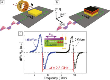
Tunable radio-frequency (RF)/microwave magnetic devices, such as tunable inductors, tunable filters, tunable resonators, and phase shifters, have been widely deployed in aircraft, satellites, and portable communication systems. Reference Sun and Srinivasan5,Reference Srinivasan64,Reference Liu and Sun65 Such tunable RF/microwave magnetic devices typically operate on the basis of a dramatic change in permeability at approximately the ferromagnetic resonance (FMR), which arises from the precessional motion of magnetization in an external magnetic field. Therefore, a current-driven electromagnet is typically necessary in these devices (see schematic in Figure 4a), which, in principle, makes them energy-consuming, bulky, noisy, and difficult for on-chip integration. In multiferroic magnetoelectric nanostructures, the permeability of the magnetic phase can alternatively be tuned by a non-power-dissipating electric field mediated by electrostrains, enabling electrically tunable RF/microwave magnetic devices with ultralow power consumption. An electric field is also easy to generate and localize on a chip, which is beneficial for device miniaturization.
Experimental setup of ferromagnetic resonance measurement for demonstrating the working principles of (a) magnetically and (b) electrically tunable radio-frequency/microwave magnetic devices, where a single-layer magnetic thin film (e.g., Co20Fe60B20 [CoFeB]) or a bilayered magnetoelectric nanostructure is laid face down on an S-shaped coplanar waveguide (CPW). The CPW generates a microwave magnetic field to excite magnetization precession in CoFeB. A DC testing magnetic field (H DC) of 720 Oe is applied along the [100] direction in both cases (not shown). (c) First derivative of the absorption power (P) with respect to H DC as a function of the frequency of the microwave magnetic field. The resonance frequencies that are determined by the intersection of the spectra and the baseline (dashed line) can be modulated by an applied electric field. The ferroelectric layer is Pb(Mg1/3Nb2/3)0.71Ti0.3O0.29 (PMN-PT). (b) Adapted with permission from Reference 65. © 2014 Royal Society Publishing. (c) Adapted with permission from Reference 66. © 2013 Wiley-VCH.

For example, in a horizontal magnetoelectric nanostructure consisting of a 20-nm-thick Co20Fe60B20 (CoFeB) film grown on top of a 500-μm-thick (011)-oriented PMN-PT layer (see Figure 4b), a small electric field of 1.5 kV cm–1 applied across the nanostructure can shift the FMR frequency of the CoFeB film by up to 2.3 GHz (see Figure 4c), Reference Liu, Howe, Grazulis, Mahalingam, Nan, Sun and Brown66 based on an electrostrain-induced change in permeability. Reference Sun and Srinivasan5 Although the use of magnetic alloys (e.g., CoFeB and FeGaB Reference Lou, Liu, Reed, Ren and Sun67 ) with large magnetostriction can lead to high strain-mediated electrical tunability, the high microwave loss of these alloy materials is an important issue. Low-loss magnetic ferrites such as epitaxial single-crystal yttrium iron garnet (YIG) have been widely used in magnetically tunable RF/microwave devices, but their smaller magnetostriction leads to lower electrical tunability. Nevertheless, it is possible to achieve reasonably high electrical tunability in YIG-based magnetoelectric nanostructures with sharp and elastically coherent interfaces. For instance, in a high-quality multilayered magnetoelectric nanostructure of YIG (300-nm-thick)–Pt (30-nm-thick)–(Ba,Sr)TiO3 (BSTO, 1-μm-thick)–Pt (50-nm-thick) grown on a single-crystal gadolinium gallium garnet substrate, Reference Das, Song, Mo, Krivosik and Patton68 a maximum electrical tunability of FMR of above 2 MHz V–1 can be achieved at 25 V, which is nearly one order of magnitude larger than that in a bulk heterostructure with a mechanically bonded YIG (7-μm-thick) layer and BSTO ceramic slab (500-μm-thick). Reference Ustinov, Tiberkevich, Srinivasan, Slavin, Semenov, Karmanenko, Kalinikos, Mantese and Ramer69
Ultralow-cost magnetic field sensors
Ultrasensitive and high-spatial-resolution magnetic field sensors are critically important to noninvasive medical imaging and diagnosis, such as magnetoencephalography (MEG, which detects magnetic fields of the brain to analyze neural activities), cardiological diagnosis, and magnetogastrography, which detects magnetic fields of the stomach. Given that the magnetic fields produced by human organs are typically weak, ranging from 10 fT to 1 pT, Reference Nakaya and Mori70,Reference Wikswo71 and have low frequencies (below 103 Hz), Reference Zhai, Xing, Dong, Li and Viehland72 magnetic field sensors with sub-picotesla sensitivity in this frequency range are desired. This leaves no option but to use ultrasensitive magnetic field sensors based on high-density arrays of a superconducting quantum interference device (SQUID), which, however, require expensive and cumbersome cryogenic systems (e.g., see a practical MEG system from the brain mapping center of University of Pittsburgh Medical Center at www.meg-brain-mapping.pitt.edu). Thus, it is imperative to develop a novel low-cost magnetic field sensor whose sensitivity is comparable to that of a SQUID-based sensor.
Multiferroic-magnetoelectric-composite-based magnetic field sensors, with ultralow cost and compact size, Reference Israel, Mathur and Scott73 have been demonstrated as among the most promising candidates. These magnetoelectric sensors allow a direct transformation (i.e., without requiring source current) of a weak AC magnetic field signal into a voltage signal over a broad temperature range (e.g., from –35°C to 85°C; see Reference Reference Ye, Ma, Ma, Hu, Li, Feng, Zhang and Nan74) through a strain-mediated direct magnetoelectric coupling (i.e., magnetically tunable polarization). Reference Nan, Liu, Lin and Chen75–Reference Wang, Li, Wang, He and Nan77 In particular, the sensitivity of magnetoelectric sensors based on bulk magnetoelectric composites Reference Zhai, Xing, Dong, Li and Viehland72 can become comparable to that of a SQUID-based sensor if the frequency of the target magnetic field is equal or close to the electromechanical resonance frequency (typically 104–105 Hz) of the constituent ferroelectric/piezoelectric material. Reference Bichurin, Filippov, Petrov, Laletsin, Paddubnaya and Srinivasan78
However, it is difficult to utilize bulk magnetoelectric composites to fabricate high-density magnetoelectric sensor arrays for biomedical use. Reference Greve, Woltermann, Quenzer, Wagner and Quandt79 More importantly, the sensitivity of existing magnetoelectric sensor prototypes is insufficient to detect low-frequency (below 103 Hz) AC magnetic fields for the following three reasons. First, the strain-mediated direct magnetoelectric response is typically low (resulting in weak magnetically induced voltage signals) if the frequency of the target AC magnetic field is far from electromechanical resonance. Second, the noise level increases significantly with decreasing frequency f because of the 1/f noise, Reference Edelstein and Fischer80,Reference Stutzke, Russek, Pappas and Tondra81 as in other types of magnetic field sensors. Third, the externally applied DC bias magnetic field, commonly used to set the piezomagnetic coefficient at a maximum to maximize the direct magnetoelectric coupling, Reference Ma, Hu, Li and Nan3,Reference Wang, Hu, Lin and Nan82 creates an additional noise source. The use of such an external bias magnetic field in high-density magnetoelectric sensor arrays would also lead to crosstalk among neighboring sensors and, hence decrease the spatial resolution.
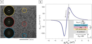
Recently, on a silicon cantilever substrate, a horizontal magnetoelectric nanostructure consisting of a magnetic multilayer of Ta/Cu/Mn70Ir30/FeCoSiB (or Fe50Co50) grown on a 2-μm-thick piezoelectric AlN layer was fabricated. Reference Lage, Kirchhof, Hrkac, Kienle, Jahns, Knochel, Quandt and Meyners83 Because of the tightly bonded interfaces at the nanoscale (see Figure 5a) and the relieved mechanical constraint from the substrate in the cantilever geometry (i.e., the multilayer is only clamped on one end, see the inset of Figure 5b), a significant amount of magnetic-field-induced strain can be obtained and transferred efficiently to the AlN, leading to a high magnetoelectric coefficient α H,31 (= dE 3/dH 1) of over 100 V cm–1 Oe–1 at a resonance frequency of 1197 Hz, which is close to the desirable frequency range below 103 Hz. Here, E 3 and H 1 indicate the induced electric field and applied magnetic field along the out-of-plane and in-plane (long axis of the cantilever substrate) directions, respectively. In particular, by exploiting the exchange bias field between the antiferromagnetic Mn70Ir30 and the ferromagnetic FeCoSiB (or Fe50Co50) in the multilayer as a built-in DC bias magnetic field, a high α H,31 value of 96.7 V cm–1 Oe–1 is obtained under zero externally applied bias magnetic field (Figure 5b), which is beneficial for achieving a low noise level and a high spatial resolution. Indeed, with this built-in bias magnetic field and the high value of α H,31, a high sensitivity limit of 10 pT Hz–1/2 was achieved at resonance frequency for the FeCoSiB-based magnetoelectric nanostructure. By optimizing the thickness and magnetic domain structure of the FeCoSiB layer, α H,31 was recently enhanced to about 430 V cm–1 Oe–1 at a lower resonance frequency of about 700 Hz, Reference Lage, Urs, Röbisch, Teliban, Knöchel, Meyners, McCord and Quandt84 which should lead to an even higher sensitivity.
(a) Cross-sectional transmission electron microscope bright-field image of a horizontal magnetoelectric nanostructure consisting of a Ta/Cu/Mn70Ir30/Fe50Co50 multilayer deposited on an AlN layer on a silicon cantilever substrate, with selected-area electron diffraction patterns of different sample areas. The asterisk inside the blue circle on the right indicates the area next to the multilayer/AlN interface. (b) The magnetoelectric voltage coefficient α H,31 as a function of the DC bias magnetic field (μ0 H DC, where the prefactor μ0 is the vacuum permeability) in the magnetoelectric nanostructure based on a Ta/Cu/Mn70Ir30/Fe70.2Co7.8Si12B10 multilayer under an excitation magnetic field (δH) with a frequency of 1197 Hz. The inset schematically shows the sample geometry and the definition of α H,31, where δV is the induced voltage and t is the thickness of the AlN layer. Adapted with permission from Reference 83. © 2012 Nature Publishing Group.

More recently, a novel nanoelectromechanical systems (NEMS) magnetoelectric resonator consisting of a multilayered AlN/(FeGaB/Al2O3) heterostructure on an etched silicon substrate was developed for detecting low-frequency AC magnetic fields. Reference Nan, Hui, Rinaldi and Sun85 In such an NEMS magnetoelectric resonator, the magnetic field can be sensed not only by electrically detecting the magnetically tunable polarization, where an external or built-in DC bias field is required, as mentioned earlier, but also by electrically detecting the magnetically tunable electromechanical resonance frequency. The latter is based on the ΔE effect Reference Ludwig and Quandt86 (i.e., magnetic-field-induced changes in the Young’s modulus of magnetic materials), and these changes are nonzero under zero DC bias magnetic field. Thus, in the latter scenario, a DC bias magnetic field is no longer required. Furthermore, the frequency of the target AC magnetic field does not have to be the same as the electromechanical frequency for the enhanced sensitivity, allowing the detection of a broadband low-frequency AC and even DC magnetic fields. Reference Nan, Hui, Rinaldi and Sun85 It is also easy to integrate such NEMS resonators with CMOS platforms to fabricate high-density magnetoelectric sensor arrays.
Outlook
The interface-based magnetoelectric coupling in multiferroic magnetoelectric nanostructures is being exploited for many exciting device technologies. Compared to bulk multiferroic magnetoelectric heterostructures, these magnetoelectric nanostructures are easier to integrate on a chip, and their interfaces can be controlled or designed for enhanced magnetoelectric coupling or new functionalities (e.g., MFTJ). Despite the bright future and notable progress, many challenges remain to be overcome before the practical use of these magnetoelectric nanostructures in the mentioned device technologies.
To compete with the complex but very effective HAMR technology, larger electric-field-induced reductions in the perpendicular magnetic anisotropy and magnetic coercive field are desirable for EAMR. This requires further enhancement of the converse magnetoelectric coupling across the magnetic–ferroelectric interface in the layered magnetoelectric composite thin film (shown in Figure 2a), which is challenging because the electric-field-induced strain would be limited by substrate clamping. One promising solution is to exploit interfacial charge-mediated converse magnetoelectric coupling, which can become effective over a long spatial scale (up to tens of nanometers) near the interface through exchange coupling Reference Zhou, Leong, Yuan, Hu, Ong and Liu22 or magnon excitation Reference Jedrecy, von Bardeleben, Badjeck, Demaille, Stanescu, Magnan and Barbier87,Reference Jia, Wei, Jiang, Xue, Sukhov and Berakdar88 and can become stronger with intervention from interfacial redox reactions. Reference Leistner, Wunderwald, Lange, Oswald, Richter, Zhang, Schultz and Fähler89–Reference Bi, Liu, Newhouse-Illige, Xu, Rosales, Freeland, Mryasov, Zhang, te Velthuis and Wang91 A more promising solution is based on high-density arrays of layered magnetic–ferroelectric nanoislands. Such novel magnetoelectric nanostructures were recently predicted to show strong strain-mediated magnetoelectric coupling due to the extraordinarily large (1% and above) electric-field-induced homogeneous strains Reference Hu, Yang, Chen and Nan29,Reference Hu, Yang, Wang, Huang, Zhang, Chen and Nan30 and, in particular, to exhibit a purely electrically driven reversal of uniform magnetization Reference Hu, Yang, Wang, Huang, Zhang, Chen and Nan30 that can be exploited for both high-density HDD (see Figure 2b) and high-density perpendicular MRAM. Both predictions remain to be verified by experiments.
For application as electrically tunable RF/microwave devices, one of the challenges is to develop magnetic materials (most likely, based on ferrites) that simultaneously exhibit low microwave loss and large magnetostriction (for high strain-mediated electrical tunability). A promising approach to achieving greater flexibility for materials selection and design is to exploit interfacial charge-mediated converse magnetoelectric coupling (as recently demonstrated experimentally Reference Nan, Zhou, Liu, Yang, Gao, Assaf, Lin, Velu, Wang, Luo, Chen, Akhtar, Hu, Rajiv, Krishnan, Sreedhar, Heiman, Howe, Brown and Sun92,Reference Zhou, Howe, Liu, Nan, Chen, Mahalingam, Sun and Brown93 ), such that large magnetostriction is no longer necessary.
It is appealing to replace the expensive and bulky SQUID-based magnetic sensor arrays with low-cost and compact-sized magnetoelectric-nanostructure-based magnetic sensor arrays for biomedical imaging and diagnosis. The high sensitivities on the order of pT Hz–1/2 for low-frequency (<103 Hz) magnetic field detection, recently achieved in self-biased multilayered magnetoelectric nanostructures, Reference Lage, Kirchhof, Hrkac, Kienle, Jahns, Knochel, Quandt and Meyners83,Reference Nan, Hui, Rinaldi and Sun85 represent important progress, but there is still a long way to go. One of the most immediate needs is to further enhance the low-frequency magnetic field sensitivity to the order of ƒT Hz–1/2: a level not far from that of SQUID-based magnetic sensors. Reference Gallop94,Reference Fagaly95 This should be pursued, on one hand, by enhancing the direct magnetoelectric coupling (e.g., by optimizing the microstructure and interfaces of such multilayered magnetoelectric nanostructures Reference Lage, Urs, Röbisch, Teliban, Knöchel, Meyners, McCord and Quandt84 or possibly by operating them in shear mode Reference Lu, Mei, Jeong, Xiang, Xie and Zhang96 ) and, on the other hand, by reducing the noise level. Reference Wang, Gao, Li, Shen, Hasanyan, Li and Viehland97
Acknowledgments
We gratefully acknowledge our colleagues and collaborators for sharing their insights and contributions, including C.W. Nan, Q.M. Zhang, C.B. Eom, D.G. Schlom, and R. Ramesh. We especially thank X.X. Cheng for help preparing the schematic figures and M.-C. Lu and M. Liu for helpful discussions. J.-M.H. and L.-Q.C. gratefully acknowledge financial support from the National Science Foundation under Grant DMR-1234096. T.N. and N.X.S. gratefully acknowledge financial support from the Air Force Research Laboratory through Contract FA8650-14-C-5706 and, in part, Contract FA8650-14-C-5705 and from the W.M. Keck Foundation.