


Introduction
Rapid developments in microelectronic devices and miniaturized sensors rely on defining small patterns at ever-decreasing length scales, which are now reaching sub-22 nm.Reference Liddle and Gallatin1 The required level of precision and complexity can be achieved using ultraviolet lithography to define deterministic pattern geometries and sequential metal/ceramic/semiconductor deposition and etching. However, these techniques are cost-efficient only up to wafer-scale sizes (<12" diameter)Reference Liddle and Gallatin1 and are less suitable for covering meter-scale areas. On the other hand, relying on the same microfabrication processes as used in microelectronics, several recent demonstrations have focused on texturing and patterning micro- and nanoscale features to study efficiency of energy transfer across interfaces,Reference Chu, Xiao and Wang2 including solar cells,Reference Pint, Takei, Kapadia, Zheng, Ford, Zhang, Jamshidi, Bardhan, Urban, Wu, Ager, Oye and Javey3 anti-wetting/icing coatings,Reference Paxson and Varanasi4 and unusual optical and acoustic metamaterials.Reference Gansel, Thiel, Rill, Decker, Bade, Saile, von Freymann, Linden and Wegener5–Reference Zhao, Belkin and Alù7 For these applications to become commercially viable, three-dimensional (3D) texturing and patterning must be possible at high throughput and with high precision on meter-scale areas. New nanofabrication techniques with the potential to address these challenges, such as roll-to-roll nanoimprint lithography, are simultaneously in development.
The deformation of slender microstructures induced by capillary forces, also known as elasto-capillary phenomena, have recently emerged as a fabrication method with the ability to locally control 3D geometries at the nanometer scale. During simple wetting and drying by water or organic solvents, elasto-capillary forces can induce the formation of complex 3D patterns (such as bent and helical structures) from simple surface features in a fast and cost-effective manner.Reference De Volder and Hart8,Reference Roman and Bico9 As a manufacturing process, they can be applied to existing straight (prismatic) structures such as straight nanopillars to transform them into freeform 3D structures with intricate curvatures along the height axis (Figure 1a).Reference Hu, Lao, Cumming, Wu, Li, Liang, Chu, Huang and Gu10 Elasto-capillary fabrication can augment the capabilities or overcome the limitations of current microfabrication processes. For example, carbon nanotube (CNT) forests, which are often synthesized with vertical orientation (perpendicular to a substrate), typically show good alignment and density, but are difficult to process using planar microfabrication techniques due to their vertical orientation (Figure 1b).Reference Copic, Park, Tawfick, De Volder and Hart11 After submerging in an organic solvent such as acetone, it is found that the nanotubes can become reoriented during the drying process to lay down flat on the substrate, enabling their use as electrical interconnects and mechanical switches.Reference Hayamizu, Yamada, Mizuno, Davis, Futaba, Yumura and Hata12,Reference Tawfick, De Volder and Hart13 Similarly, in microelectromechanical systems (MEMS), 2D patterns and thin films can be pursued on horizontal flat wafers by photolithography and metal liftoff. Subsequently, using capillary-activated hinges, these in-plane panels can be tilted to the vertical (out-of-plane orientation).Reference Vaccaro, Kubota, Fleischmann, Saravanan and Aida14–Reference Leong, Zarafshar and Gracias16
Elasto-capillary forming as a 3D lithography process. (a) Left (scale bar 5 µm), straight nanopillars with 700-nm diameter and 2.5-µm height (inset scale bar 700 nm) are fabricated by femtosecond laser-assisted lithography. Right image (scale bar 10 µm) demonstrates the capillary induced self-assembly of three-pillar clusters into “tepees.”Reference Hu, Lao, Cumming, Wu, Li, Liang, Chu, Huang and Gu10 (b) Left image shows an assembly of vertically aligned carbon nanotubes (CNTs), where the individual CNT diameter is 10 nm, and the microstructure height is 70 µm. After the condensation and evaporation of acetone, the microstructure folds, laying down flat on the substrate (scale bar 10 µm) while retaining the alignment of the CNTs (inset scale bar 700 nm).Reference Copic, Park, Tawfick, De Volder and Hart11

From a process perspective, elasto-capillary lithography lies at the intersection of two major nanofabrication processes: self-assembly and strain engineering.Reference Leong, Zarafshar and Gracias16,Reference Whitesides and Grzybowski17 Self-assembly allows local short-range surface forces of micro- to nanoscale particles to self-organize, while strain engineering uses residual stresses to locally cause geometric changes such as wrinkling and bending.Reference Bowden, Brittain, Evans, Hutchinson and Whitesides18
This article is organized as follows: the next section briefly presents the physical ingredients of elasto-capillary phenomena such as buckling and aggregation. The following section presents some of the successful applications of elasto-capillary fabrication. The final section addresses some current challenges and opportunities of this exciting field.
The elasto-capillary phenomenon
Children learn early, while painting, how to dip a disordered brush into a glass of water in order to assemble the uneven hairs into the desired point. More tragically, the hydrophobic barbules of seabird feathers also form bundles as they come in contact with an oil spill.Reference Duprat, Protiere, Beebe and Stone19 In both situations, the attraction between flexible fibers results from a balance between capillary forces and elasticity (i.e., the interactions that respectively dictate the spherical shape of water droplets and the stiffness of fibers). Such surface forces become dominant at small scales, and they may induce the failure of engineered microstructures. As a practical example, the tiny accelerometers present in high-tech devices such as smart phones rely on micron-sized cantilever beams whose deflection can be blocked by moisture-induced capillary stiction.Reference Maboudian and Howe20 Due to such fatal effects, capillary forces are usually viewed as a limitation in traditional microfabrication technology.Reference Maboudian and Howe20 However, recent developments involving controlled self-assembly are progressively bringing a more optimistic paradigm. Capillary forces are, for instance, commonly used to self-align chips in welding facilities,Reference Lambert, Mastrangeli, Valsamis and Degrez21 and “capillary origami” has been proposed as a tool to deploy planar templates into 3D microstructures.Reference Roman and Bico9,Reference Leong, Zarafshar and Gracias16,Reference Legrain, Janson, Berenschot, Abelmann and Tas22 Motivated by recent experiments on substrates covered with micropillarsReference Hu, Lao, Cumming, Wu, Li, Liang, Chu, Huang and Gu10,Reference Fan, Dyer, Zhang and Zhao23–Reference Grinthal, Kang, Epstein, Aizenberg, Khan and Aizenberg28 or nanotubes,Reference De Volder and Hart8,Reference Chakrapani, Wei, Carrillo, Ajayan and Kane29,Reference Liu, Li, Zhai, Li, Zheng, Jiang and Zhu30 we focus here on the self-patterning of surfaces with vertical slender structures.
Slender structures such as fibers or thin plates are prone to deflect or to buckle as a lateral force or a compressive load is respectively applied. At which scale will capillary forces be strong enough to bend such a structure? Consider a single circular microrod clamped on a substrate and immersed in a liquid (e.g., the solvent used to remove uncured resin in a photolithography process). As the liquid evaporates, its surface eventually reaches the tip of the rod (see Figure 2a). Does the rod pierce the interface without bending? Piercing through the interface leads to the formation of a meniscus around the rod. The corresponding capillary force acting on the rod is given by F cap = 2πrγcosθ, where r is the radius of the rod, γ is the liquid/air surface tension, and θ is the contact angle of the liquid on the rod. The rod is thus expected to buckle if its length, L, exceeds the critical limit determined by Euler,
 $${L_c}\, = \,{\pi \over 2}\sqrt {{{EI} \over {{F_{cap}}}}}$$,
where E is the Young’s modulus, and I is the second moment of inertia of the beam,  $I\, = \,{{\pi {r^{\rm{4}}}} \over 4}$. In terms of scaling, the critical length is proportional to
 $${L_{EC}}\, = \,\sqrt {{{E{r^3}} \over \gamma }}$$,
which we refer to as the elasto-capillary length; 1/L EC sets the curvature that surface tension forces can induce on a flexible structure.Reference Roman and Bico9,Reference Cohen and Mahadevan31,Reference Liu and Feng32 This length scale applies to a broad range of materials from nanotubes, to polymer and metallic nanostructures. In addition, the bending direction of the pillars may be controlled by tuning the shape of their cross section.Reference Chae, Güneş, Kim, Kim, Han, Kim, Shin, Yoon, Choi, Park, Yang, Pribat and Lee33,Reference Duan, Yang and Berggren34
(a) Buckling of a rod (radius, r) induced by capillary forces (F) if the length of the rod exceeds a critical value L C proportional to the elasto-capillary length L EC. (b) Stiction of a pair of fibers clamped at a distance d by a capillary bridge if their length is larger than  ${L_{\min }} \sim \sqrt {d{L_{EC}}}$. (c) Hierarchical bundling of a macroscopic brush. Pairs of smaller units are successively associated into larger bundles until reaching the final size N.Reference Py, Bastien, Bico, Roman and Boudaoud37 (d) Alternative scenario involving a single-step clustering if the length of the fibers exceeds L s ∼(Er 2d 2/γ)1/3.Reference Chandra and Yang38,Reference Zhao and Fan39
The effect of capillarity is not limited to buckling. Capillary forces may also induce the bundling of dense arrays of fibers. Experiments conducted with macroscopic brushes have shown that bundling dynamics lead to hierarchical structures, where pairs of smaller units are successively associated into larger bundles.Reference Bico, Roman, Moulin and Boudaoud35,Reference Kim and Mahadevan36 The adhesion of a pair of fibers separated by a distance d involves a minimal curvature on the order of d/L 2. If this curvature is smaller than 1/L EC (i.e.,  $L\, &gt; \,{L_{min}} \sim \sqrt {{L_{EC}}d}$), the fibers are prone to stick together (Figure 2b). The same law also predicts stiction of microcantilevers if the radius r in the definition of L EC is replaced by the thickness of the cantilevers. This relation can be adapted to describe the association of a pair of bundles containing N/2 fibers leading to a bundle of size N (Figure 2c). In this case, the effective stiffness of each bundle is multiplied by N/2, while their distance of separation is amplified by a factor proportional to
 $\sqrt N$ (for a 2D lattice). As a consequence, a bundle of fibers of length L and spacing d can be formed at the condition
 $L\, &gt; \,{L_{\min }}\left( N \right) \sim {N^{3/8}}\sqrt {{L_{EC}}d}$. In other words, the maximum size of a bundle composed of fibers of length L is
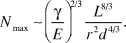 $${N_{\max }} \sim {\left( {{{{\gamma ^{}}} \over {\rm E}}} \right)^{2/3}}\,{{{L^{8/3}}} \over {{r^2}{d^{4/3}}}}\.^{37}$$
An alternative scenario considers a one-step clustering where fibers simultaneously associate (Figure 2d),Reference Chandra and Yang38 which is highly relevant for the case of fibers of moderate aspect ratio (r/L ∼ 0.1).Reference Chandra and Yang38–Reference Chandra and Yang40 The model is based on the lateral attraction between liquid menisci formed as the fibers pierce the interface. The corresponding surface energy approximately scales as γr 2, while the bending energy of a fiber is proportional to  $E{r^4}L{\left( {{{{N^{1/2}}d} \over {{L^2}}}} \right)^2}$. The maximum bundle size is finally given by N max ∼(L/L s)3, with
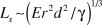 ${L_s}\, \sim \,{\left( {E{r^2}{d^2}/\gamma } \right)^{1/3}}$. In practice, complex dynamics lead to a broad size distribution. Nevertheless, the lower bound of this distribution, N min, remains proportional to N max for both scenarios.
When carpets of CNTs or other arrays of flexible micropillars are dipped into a solvent and then dried, two types of structures are usually observed: bundles or cellular patterns (Figure 3a).Reference Correa-Duarte, Wagner, Rojas-Chapana, Morsczeck, Thie and Giersig41 The selection between each mode relies on a combination of the two mechanisms previously described (Figure 3b).Reference Chiodi, Roman and Bico42 Capillary forces first lead to the formation of aggregates of size N (N min < N < N max). Although bundles are stiffer than individual pillars, they may buckle if their length exceeds a critical size L c(N). We thus expect to observe bundles for L c(N min) < L and large bundles surrounded by collapsed pillars for L c(N min) < L < L c(N max). In the extreme situation of short pillars (N < 2 and L < L c(1)), the structure remains unchanged. Conversely, long pillars (L > L c(N max)) all collapse.
(a) Scanning electron microscope images of bundles (top) or cellular (bottom) patterns formed as a carpet of carbon nanotubes is dipped into a solvent and dried.Reference Correa-Duarte, Wagner, Rojas-Chapana, Morsczeck, Thie and Giersig41 (b) Configuration diagram obtained with one-dimensional model brushes as a function of brush length (L) and separation (d), normalized with respect to the elasto-capillary length L EC. Capillary forces lead to bundles of N brushes (N min to N max), with major configuration changes occurring at critical lengths, L crit-, as a function of N.Reference Chiodi, Roman and Bico42
Capillary forces induce the formation of self-assembled structures. In the absence of any specific adhesion strategy (e.g., initially dissolved polymeric molecules acting as glue), attractive van der Waals interactions may maintain the structure.Reference Chandra and Yang38,Reference Glassmaker, Jagota, Hui and Kim43–Reference Delrio, De Boer, Knapp, Reedy, Clews and Dunn45 When the magnitude of the corresponding adhesion energy is comparable to the elastic bending energy of liquids, the structures are expected to persist after they are dried. In the case of adhesion between polymeric structures, the attraction is significantly increased by plasma treatment, which adds functional hydroxyl groups.Reference Kang, Pokroy, Mahadevan and Aizenberg46 However, the effective adhesion energy is qualitatively different in the case of rod geometries.Reference Roca-Cusachs, Rico, Martínez, Toset, Farré and Navajas44,Reference Chaudhury, Weaver, Hui and Kramer47 As parallel soft fibers are adhering along their length, their contact area relies on a balance between adhesion energy and elastic deformation of the cross section of the rods. The corresponding contact width is given by  $a \sim {\left( {{{{W_{ad}}} \over E}{r^2}} \right)^{1/3}}$, where W ad is the van der Waals adhesion energy. If a liquid column initially bridges the rods along a length L, the initial capillary energy scales as rLγ. In the case of dry adhesion, this energy becomes
 $aL{W_{ad}} \sim rL{W_{ad}}{\left( {{W_{ad}}/Er} \right)^{1/3}}$. Soft and thin fibers thus promote strong stiction.
These principles represent the fundamental physical ingredients promoting elasto-capillary self-assembly. We next present some practical examples ranging from bundles to chiral structures and then focus on possible applications.
Design of textured surfaces by elasto-capillary engineering
One of the earliest observations of the elasto-capillary effect in nanoscale materials was the increased density of nanotubes, pillars, or wires obtained by “zipping” them together (Figure 3a).Reference Chakrapani, Wei, Carrillo, Ajayan and Kane29,Reference Liu, Li, Zhai, Li, Zheng, Jiang and Zhu30,Reference Futaba, Hata, Yamada, Hiraoka, Hayamizu, Kakudate, Tanaike, Hatori, Yumura and Iijima48 For example, a CNT “forest” or “mat” is a configuration where individual CNTs are aligned with one another and oriented perpendicular to the substrate; they are hence called vertically aligned (VA-) CNTs. This form of CNTs affords precise control over the CNT length and diameter, from 1-nm single-walled to 20-nm multi-walled CNTs, as well as good alignment among the CNTs.Reference Yamada, Namai, Hata, Futaba, Mizuno, Fan, Yudasaka, Yumura and Iijima49 However, the solid density in CNT forests is very low, usually 1–5 vol%, which make them fragile and unsuitable for mechanical or wet chemical post-processing. Simply immersing CNT forests in a liquid such as water or acetone then drying changes their configuration to “tepees” or, depending on the structure of the forest, to a cellular foam with cell walls and ridges consisting of dense and mechanically stable aligned CNTs (Figure 3a).
The formation of microcellular structures sheds light on some important practical considerations in elasto-capillary aggregation: The interplay between the nanotubes’ height, modulus, and adhesion to the substrate determines the maximum size of uniform aggregates that can be formed.Reference Chiodi, Roman and Bico42 The scaling laws described earlier are derived assuming ideal bonding of the CNTs to the substrate, which is critical but challenging to realize in practice. Nonetheless, by carefully patterning hierarchical CNT micropillars, composed of a large number of aligned nanotubes with diameters from 10–100 μm and aspect ratios from 1–10, De Volder et al. fabricated dense and uniform vertical interconnects with good mechanical and electrical properties that could be further mechanically reinforced by simple spin-coating of a polymer to form polymer-CNT composite microstructures (Figure 4a–c).Reference De Volder, Tawfick, Park, Copic, Zhao, Lu and Hart50 VA-CNT pillars synthesized by chemical vapor deposition with semicircular cross sections bend (Figure 4a), while those with chiral, flower-like cross sections twist to form helices (Figure 4b), and those with hollow, cylindrical cross sections collapse to form flat, radially aligned CNT sheets when dried (Figure 4c).Reference De Volder, Tawfick, Park, Copic, Zhao, Lu and Hart50 Fortunately, these structures obtained from capillary densification and geometrical transformations are mechanically more robust, and thus overcome some of the limitations of as-synthesized low density fibrous nanomaterials.
Elasto-capillary design of large-area 3D textures from straight nanotubes and nanopillars. Top panel (a–c) shows schematics and accompanying scanning electron microscope (SEM) images of a variety of 3D microstructures, each comprising thousands of vertically aligned carbon nanotubes: (a) inward and outward bending microbeams (scale bars 40 μm), helices (scale bar 40 μm), and straight hollow microneedles concentric with radially aligned annular rings (scale bar 20 μm).Reference De Volder, Tawfick, Park, Copic, Zhao, Lu and Hart50 (d–g) SEM images of straight polymer bristles and their long- and short-range order. (d) As-prepared straight pillars with 250-nm diameter and 8-μm height (scale bar 1 μm); (e–f) self-assembly of pillars and the creation of chiral clusters (bottom scale bar 400 nm); and (g) meniscus lithography applied to achieve long-range moiré-like order by laminating two identical bristle surfaces with a small bias angle θ (scale bar 50 μm, inset scale bar 10 μm).Reference Pokroy, Kang, Mahadevan and Aizenberg24,Reference Kang, Wu, Grinthal and Aizenberg52
Elasto-capillary forces can reorient vertical CNTs into horizontally aligned, mechanically stable films (Figure 1b).Reference Hayamizu, Yamada, Mizuno, Davis, Futaba, Yumura and Hata12 Starting from high-aspect-ratio line patterns, MEMS cantilevers were fabricated from horizontally aligned CNTs based on this process. Tawfick et al. demonstrated that the folding direction can be programmed to arbitrary directions, independent of the immersion liquid front.Reference Tawfick, De Volder and Hart13 Similarly, Duan et al. utilized a symmetry breaking approach to self-fold high-aspect-ratio polymer arcs of <50 nm width into deterministic patterns.Reference Duan and Berggren51 They studied the effects of the arc angle and radii, and ultimately obtained large arrays of self-folding in a controlled direction. This also allowed them to control the narrow gaps (or slits) formed between the fins after they collapse.
General interest in helices stems from their ability to control light polarization and propagation, such as in optical metamaterials,Reference Zhao, Belkin and Alù7 as well as their mechanical properties for flexible electrical and thermal conductors. Pokroy et al.’s pioneering work (Figure 4d–f) obtained hierarchically helical nanobristles by elasto-capillary deformation of straight epoxy posts, and demonstrated their use in trapping microparticles.Reference Pokroy, Kang, Mahadevan and Aizenberg24
One notable limitation is the difficulty in achieving long-range order, even in periodic and symmetric pillars, and especially for high-aspect-ratio pillars, where the pillar height allows interaction with the second nearest neighbor.Reference Hu, Lao, Cumming, Wu, Li, Liang, Chu, Huang and Gu10 This manifests itself as self-assembled pillars of variable cluster sizes and sometimes non-uniform geometry (Figure 4e). A novel approach to solve this problem is templated drying, for example, by confining a meniscus between two identical substrates with periodic nanopillars.Reference Kang, Wu, Grinthal and Aizenberg52 Kang et al. showed that using this meniscus lithography approach, and by controlling the bias angle between the two substrates, a moiré-like pattern can be locally formed (Figure 4g), leading to local chiral organization of pillars in the short range, and periodic repeating in the long range.
Applications
As described previously, elasto-capillary-driven self-organization expands the capabilities of conventional lithographic approaches, and enables the fabrication of complex geometries or extreme nanoscale spacing. These structures are not just curiosities, but have a number of interesting applications in diverse fields, including chemical and biological sensing, modifying surface optical properties, mechanical switches and resonators, and electrical interconnects. For example, periodic arrays of hydrogel micropillars, often with some color due to Bragg diffraction, can be collapsed into randomized clusters promoting random scattering of light and leading to a whitening layer, as shown in Figure 5a.Reference Chandra, Yang, Soshinsky and Gambogi53 Compared to alternative whitening layers, which often require layers greater than 100 μm thick and the inclusion of pigments or fluorescent dyes, this process provides the potential for comparable whiteness and brightness values in a much thinner layer.Reference Vukusic, Hallam and Noyes54 In another example, condensed CNT arrays were used as a back contact for photovoltaic solar cells, as shown in Figure 5b. With proper design of the initial CNT arrangement, the condensed arrays yield additional functionality as a scaffold for an antireflection layer, leading to enhanced light absorption in the active region of the device.Reference Pint, Takei, Kapadia, Zheng, Ford, Zhang, Jamshidi, Bardhan, Urban, Wu, Ager, Oye and Javey3
(a) Hydrogel micropillars are collapsed into random clusters, generating an ultrathin whitening layer, with scanning electron microscope (SEM) images (left) and optical images (right).Reference Chandra, Yang, Soshinsky and Gambogi53 (b) Condensed carbon nanofiber arrays (separation, d, and height, L) serve as a bottom electrode and scaffold for a back antireflection coating for solar cells. Scale bars are 3 μm.Reference Pint, Takei, Kapadia, Zheng, Ford, Zhang, Jamshidi, Bardhan, Urban, Wu, Ager, Oye and Javey3 (c) Engineered collapse of gold-coated nanopillars into pentamers for uniform and strong surface-enhanced Raman spectroscopy enhancement. Scale bars are 1 μm.Reference Kim, Ou, Ohlberg, Hu, Williams and Li62 (d) Schematic of trapping and releasing of microparticles with corresponding optical images (left) and SEM images (right). Scale bars are 3 μm.Reference Hu, Lao, Cumming, Wu, Li, Liang, Chu, Huang and Gu10
One of the most compelling applications of patterning dimensions not achievable by conventional lithography is in the field of surface-enhanced Raman spectroscopy (SERS). Capillary forces can locally increase the density of nanofibers by forming the “tepee” geometry, which could enable SERS (Figure 5c).Reference Barcelo, Kim, Wu and Li55 Some of the strongest Raman enhancement comes from metallic nanoparticles with spacing on the order of 2 nm or less due to the formation of an intense plasmon resonance.Reference Hao and Schatz56,Reference Wustholz, Henry, McMahon, Freeman, Valley, Piotti, Natan, Schatz and Van Duyne57 Because this narrow spacing is prohibitively challenging to achieve via traditional lithography, the most common approach has been to rely on random agglomeration of nanoparticles from solution. This can lead to the generation of hot spots with high Raman enhancement, but its random nature leads to poor repeatability and uniformity.Reference Fang, Seong and Dlott58 Alternatively, nanoscale polymer pillars can be patterned to collapse together in a controlled fashion under elasto-capillary forces, as shown in Figure 5c.Reference Kim, Barcelo, Williams and Li59 When the pillar tips are coated with metal, the collapsing behavior leads to the formation of regular clusters of metallic nanoparticles with nanoscale spacing.Reference Hu, Ou, Wu, Naumov, Li, Bratkovsky, Williams and Li60 This approach enables fine control over the size and shape of both the individual nanoparticles and the assembly.Reference Ou, Hu, Naumov, Kim, Wu, Bratkovsky, Li, Williams and Li61 Furthermore, the collapsing nanopillars have been shown to trap analyte molecules in the gap between adjacent particles, precisely where the strongest Raman enhancement is found.Reference Kim, Ou, Ohlberg, Hu, Williams and Li62
Trapping on the microscale also has a number of potential applications in chemistry, medicine, and microfluidics. Hu et al. have demonstrated that arrays of micropillars can be designed with appropriate height and spacing to selectively trap and release microparticles, as shown in Figure 5d.Reference Hu, Lao, Cumming, Wu, Li, Liang, Chu, Huang and Gu10 In the trapping process, size selectively arises from the fact that particles that are too large are excluded from the collapsing pillars, while particles that are too small can slip between the pillars and escape. Untrapped particles can then be removed by blowing or rinsing. Submersion in an appropriate liquid causes the pillars to reopen, leading to controlled release of the trapped particles.
Outlook
This review focused on capillary force-driven assembly of standing (or straight) nanotubes and pillars into a variety of 3D geometries, to form tailored surface textures and enable new applications. In the next few years, we expect elasto-capillary phenomena to become an engineering process in 3D lithography, overcoming the limitations of current micro- and nanofabrication in creating energy-efficient surfaces and complex biochemical microdevices. Before this becomes a reality, there is a need for precise and adaptable models that can capture the process parameters governing this process, such as the evolution of surface interactions and mechanical properties of the textures at the wet and dry states; this could enable the design of more robust textures and stable surface functionalization.
While these techniques can be useful for lab-on-chip or device-level applications, nanopillars fabricated by standard microfabrication techniques are often not cost-effective for very large areas. Application and commercialization of large areas of such textures will rely on design for manufacturability, including process integration with developing nanofabrication techniques such as roll-to-roll nanoimprint lithography, and the development of such coatings in forms that could be easily laminated onto a variety of surfaces such as glasses, metals, and composite materials.
Acknowledgments
S.T. acknowledges funding by the Mechanical Science and Engineering Department at the University of Illinois at Urbana-Champaign. J.B. acknowledges partial funding by the IAP 7/38 MICROMAST program initiated by BELSPO.



