INTRODUCTION
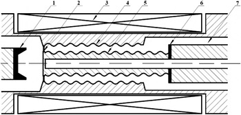
Increasing the output efficiency is a key point for the development of the relativistic backward wave oscillator (RBWO) (Swegle & Benford, Reference Swegle and Benford1998; Eltchaninov et al., Reference Eltchaninov, Korovin, Rostov, Pegel, Mesyats, Rukin, Shpak, Yalandin and Ginzburg2003), which is one of the most promising high power microwave (HPM) source devices (Benford et al., Reference Benford, Swegle, Schamiloglu, Benford, Swegle and Schamiloglu2006; Liu et al., Reference Liu, Yin, Ge, Zhan, Chen, Feng, Shu, Zhang and Wang2007). Recent progress on RBWO with the coaxial slow-wave structure (SWS) as shown in Figure 1 presents a practical approach to achieve the high output efficiency (Liu, Reference Liu2002). The numerical simulation predicted the output efficiency up to 37% (Liu et al., Reference Liu, Xiao, Chen, Shao, Hu and Wang2008; Teng et al., Reference Teng, Xiao, Song, Sun, Chen and Shao.2011). However, the introduction of coaxial rippled inner conductor not only greatly increases the output efficiency, but also results in the severe problem of power capacity, which is likely to induce the phenomenon of the pulse shortening. Since the development of the coaxial RBWO, the pulse shortening is considered to be one of the most serious problems limiting its application (Liu, Reference Liu2002).
Structure of coaxial RBWO. (1) annular cathode; (2) anode foil; (3) guide magnet solenoid; (4) outer SWS; (5) inner SWS; (6) electron collector; (7) output waveguide.

Pulse shortening was first put forward by Mesyats, Voronkov and their colleagues as an important problem that limits output energy to 10 J in Cherenkov generators and to several hundred joules in over-moded systems (Voronkov et al., Reference Voronkov, Loza and Strelkov1991). Therefore, it has become an important issue to enhance the power capacity to eliminate the pulse shortening of the HPM source device for the researchers (Korovin et al., Reference Korovin, Kurkan, Loginov, Pegel, Polevin, Volkov and Zherlitsyn2003; Li et al., Reference Li, Yuan, Zhang, Shu and Zhang2008, Reference Li, Shu, Yuan, Zhu, Liu, Wang and Zhang2010). The reasons for the pulse shortening in RBWO are rather diverse, including radio frequency (RF) breakdown, unexpected plasma generation, poor vacuum and cleanliness, electron streaming, variation of diode voltage, and so on (Benford & Benford, Reference Benford and Benford1997; Goebel, Reference Goebel1998; Korovin et al., Reference Korovin, Mesyats, Pegel, Polevin and Tarakanov2000). However, our research indicates that the electron beam interruption and combining effects of the explosive field electron emission, and the secondary electron multipactor on the surface are two main causes accounting for pulse shortening in the coaxial RBWO. It is reported that in the conventional hollow RBWO, the electric field on the surface of the X-band RBWO gets close to 1 MV/cm on the power level of 1 GW (Jin et al., Reference Jin, Zhang, Yang, Zhong, Qian, Shu, Zhang, Zhou and Xu2011; Zhang et al., Reference Zhang, Jin, Yang, Zhong, Shu, Zhang, Yuan, Li, Fan, Zhou and Xu.2010). And in such a strong field the explosive emission on the surface of SWS will occur in 10 ns (Gunin et al., Reference Gunin, Klimov, Korovin, Kurkan, Pegel, Polevin, Roitman, Rostov, Stepchenko and Totmeninov1998a). Thus, the introduction of the coaxial rippled inner conductor, which reduces the transverse cross-section of RBWO, makes the electric field much more intensive. Consequently, the explosive field electron emission and the secondary electron multipactor on the SWS surface will happen more easily, which leads to the cessation of the microwave output (Jin et al., Reference Jin, Zhang, Yang, Zhong, Qian, Shu, Zhang, Zhou and Xu2011). Besides, the special structure of the coaxial inner and outer rippled conductors, which is equipotentially connected, is likely to disrupt the beam transmission in the coaxial SWS. The beam transmission will be also disturbed by the high field (Agee, Reference Agee1998). Beam disruption will degrade the coupling of the electron beam and the electromagnetic modes of the electrodynamic structure and terminate the microwave generation (Schamiloglu, Reference Schamiloglu1999). As a result, pulse shortening becomes a serious difficulty hindering the enhancement of the output energy and the practical use of RBWO.
Since the coaxial RBWO has been put forward, most study concentrates on the numerical simulation that improves the structure in order to achieve the higher output efficiency (Teng et al., Reference Teng, Liu, Shao and Tang2008; Xiao et al., Reference Xiao, Teng, Chen and Sun2011). And little work has focused on the elimination of pulse shortening in the coaxial RBWO. Up to now, a series of researches on pulse shortening were devoted into the transient behavior of RF breakdown and plasma generation in RBWO (Chang et al., Reference Chang, Liu, Fang, Tang, Huang, Chen and Zhang2010; Price & Benford, Reference Price and Benford1998; Min et al., Reference Min, Jung, Shin, Park, An, Lee, Yoon, Kim, Lee and So2008). However, this paper describes our approach to eliminate the pulse shortening in coaxial RBWO by theoretical analysis and structure optimization, which is validated by the following experiment results.
PHYSICS DESIGN AND ANALYSIS
Coaxial SWS
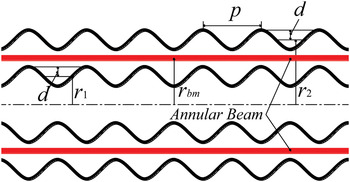
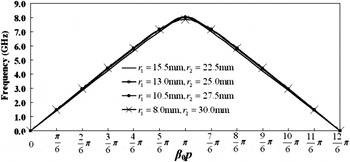
On the same level of the generation power, increasing the transverse dimension of the hollow RBWO is proved to be an effective method to lower the maximum electric field on the metallic wall, which drops as (D/λ)−2, where D is the average diameter of hollow RBWO and λ is the wavelength (Jin et al., Reference Jin, Zhang, Yang, Zhong, Qian, Shu, Zhang, Zhou and Xu2011). In the coaxial SWS as demonstrated in Figure 2, increasing the transverse cross-section has little effect on the dispersion relation of the quasi-TEM mode, which interacts with the electron beam in the coaxial RBWO (Teng et al., Reference Teng, Tang, Liu, Chen and Shao2009). It is shown in Figure 3 that while the difference between the average inner and outer radii |r 2 − r 1| increases from 7 mm to 22 mm, the variation of the frequency at π point is less than 0.2 GHz. This allows researchers to increase the transverse cross-section of coaxial RBWO without changing the output frequency.
(Color online) Structure of coaxial SWS and its key parameters, inner and outer average radii r 1 and r 2, ripple depth d, ripple period p, and radius of the infinitely thin annular beam r bm.

Effect of difference between average inner and outer radii r 1 and r 2 on dispersion relation of quasi-TEM mode in coaxial SWS. Ripple period p = 16 mm and ripple depth d = 2 mm.

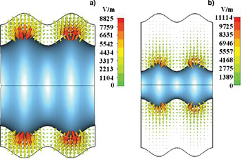
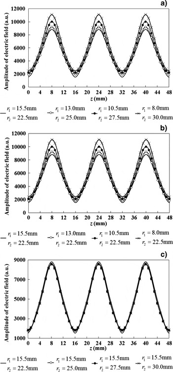
However, our researches indicate the maximum electric field in the coaxial RBWO appears on the surface of the rippled inner conductor, but not on the outer conductor as in the conventional hollow RBWO. And if the transverse distance between the average inner and outer radii r 1 and r 2 is too large, the uniformity of the field distribution in the coaxial SWS will be destroyed, which makes the electric field trend to concentrate on the rippled inner conductor as shown in Figure 4. As a result, when r 1 is reduced, the strength of the electric field on the surface of the rippled inner conductor even rises slightly as shown in Figures 5a and 5b. And when we increase r 2 with the same r 1, the amplitude of the electric field decreases a little as shown in Figure 5c, which presents some possibility of the reduction of electric field on the surface of the inner conductor.
(Color online) Electric field distribution close to π point of quasi-TEM mode in coaxial RBWO, in which ripple period p = 16 mm, ripple depth d = 2 mm. (a) r 1 = 15.5 mm; r 2 = 22.5 mm; (b) r 1 = 8 mm, r 2 = 30 mm.

Electric field of quasi-TEM mode close to π point on the radius r = r 1 + d + 0.2 mm with different average inner and outer radii r 1 and r 2. Ripple period p = 16 mm and ripple depth d = 2 mm.

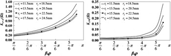
When we expand the transverse cross-section 2π(r 22 − r 12) by increasing the average inner and outer radii r 1 and r 2 together with the same |r 2 - r 1|, the concentration of the electric field on the inner conductor can be alleviated. So the amplitude of the electric field abates with the expansion of the transverse cross-section as shown in Figure 6. Nevertheless, the coupling impedances of the first harmonic and the fundamental harmonic, Kc ,-1 and Kc ,0, decline with the increment of r 1 and r 2 as shown in Figure 7, which will be likely to decrease the output efficiency. Thus, there is a trade-off between the power capacity and the output efficiency and this should be considered carefully.
Electric field of quasi-TEM mode close to π point on the radius r = r 1 + d + 0.2 mm when average inner and outer radii r 1 and r 2 are increased together. Ripple period p = 16 mm and ripple depth d = 2 mm.

Effect of increment of r 1 and r 2 on coupling impedances of -1st harmonic and fundamental harmonic K c,-1 and K c,0 in coaxial RBWO.

According to the discussion above, in the recent research on the coaxial RBWO, the applied transverse dimensions are always large, and the experimental output efficiency is lower than 18% (Ge et al., Reference Ge, Zhong, Qian, Zhang, Fan, Shu and Liu2009).
Application of Resonant Reflector
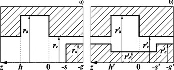
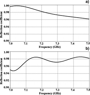
In Figure 1, the anode foil equipotentially connects the inner and outer conductors serving as the anode and prevents the microwave from propagating into the diode region. However, in the experiment under the beam bombardment the foil will produce anode plasmas, which will result in the cathode gap closure and the phenomenon of impedance collapse (Roy et al., Reference Roy, Menon, Mitra, Kumar, Kumar, Sharma, Mittal, Nagesh and Chakravarthy2008). It interrupts the beam transmission, which will reduce the output efficiency and result in the pulse shortening. Thus, we suggest replacing the anode foil by resonant reflectors as shown in Figure 8, in which the two models are connected to SWS at z = −g or z = −g′ at the right end. The reflection coefficients of the both resonant reflectors calculated through field matching method are illustrated in Figure 9, which indicates that the both resonant reflectors reflect the microwave well in the frequency range from 7.0 GHz to 7.5 GHz.
Physical models of two kinds of promising resonant reflector for coaxial RBWO. r b = 34 mm, r c = 20.5 mm, r a = 17.5 mm, h = 20 mm, s = 10 mm, r′b = 29.5 mm, r′d = 10 mm, r′c = 20.5 mm, r′a = 17.5 mm, h′ = 6 mm, s′ = 20 mm.

Reflection coefficients of both resonant reflectors in Figure 8.

Compared with the anode foil, the resonant reflector not only prevents microwave from propagating to the diode region and disturbing the generation and the transmission of the electron beam, but also pre-modulates the electron beam before it travels into the SWS (Gunin et al., Reference Gunin, Korovin, Kurkan, Pegel, Rostov and Totmeninov1998b). Pre-modulation of the electron beam can effectively enhance the output efficiency. Our researches indicate that the resonant reflector in Figure 8b can pre-modulate the electron beam efficiently. With the same coaxial SWS, employing the resonant reflector in Figure 8a the output efficiency of 36% is obtained, while employing that in Figure 8b the output efficiency can achieve up to 43% (Teng et al., Reference Teng, Liu, Shao and Tang2008).
However, the further research indicates that the resonant reflector in Figure 8b may be severely impacted by the problem of the power capacity. The resonant reflector can be considered as an open resonant cavity when the power loss on the metallic surface is neglected. And the strength of the electric field in it is closely associated with its external quality factor Q, which is defined as
 $$Q = \displaystyle{{2{\rm \pi} fW} \over P},$$
where f and P are the operation frequency and the generation power. W, the electromagnetic energy storied in the resonant reflector, can be expressed as
 $$W = \displaystyle{1 \over 2}{\rm \varepsilon} _0 \mathop{\vint \vint \vint}\limits_{ V} {\left\vert {\vec E\left({r\comma \; {\rm \theta} \comma \; z} \right)} \right\vert ^2 rdrd{\rm \theta} dz} \propto \bar E^2 {\rm \lambda} ^3 \propto \displaystyle{{\bar E^2 } \over {\,f^3 }},$$
 $\vec E\left({r\comma \; {\rm \theta} \comma \; z} \right)$ is the electric field vector in the open resonant cavity and its average amplitude is
 $\bar E$. λ is the wavelength. From Eqs. (1) and (2) it can be concluded that
 $$\bar E \propto f\sqrt {PQ}$$
According to Eq. (3), the smaller the external quality factor Q is, the lower the electric field in the open resonant cavity will be. At the operation frequency, the external quality factor of the resonant reflector shown in Figure 8a is Qa = 9.1, compared with that in Figure 8b is Qb = 20.9. It can be predicted that the electric field in the resonant reflector shown in Figure 8a is lower than that in the resonant reflector shown in Figure 8b. This is in the good agreement with the scalar field distribution in Figure 10. Therefore, it is suggested that the resonant reflector with low external quality factor Q (≤10) should be chosen to minimize the unavoidable increase of electric field in the reflector region (Gunin et al., Reference Gunin, Klimov, Korovin, Kurkan, Pegel, Polevin, Roitman, Rostov, Stepchenko and Totmeninov1998a).
(Color online) Scalar distribution of electric field in resonant reflectors (a) and (b) illustrated in Figure 8.

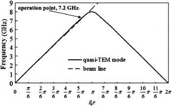
According to the conclusion above, the average inner and outer radii are optimized to be r 1 = 15.5 mm and r 2 = 22.5 mm as shown in Figure 1. The ripple period and the ripple depth are p = 16 mm and d = 2 mm, respectively. The dispersion curve of the coaxial SWS with the beam line of 500 keV is shown in Figure 11. The operation point, which is determined by the intersection of the beam line and the fundamental harmonic branch of the quasi-TEM mode, is at the 7.2 GHz close to the π mode. In the hot dispersion shown in Figure 12, the structure wave and the slower space charge wave merge into a complex conjugate pair of solution whose imaginary part represents the temporal growth rate in the range of β0p from 0 to π (Teng et al., Reference Teng, Xiao, Liu, Tang, Chen and Shao2010). The fast space charge wave interacts with the electron beam without energy exchange. The maximum of temporal growth rate ωi, max = 4.0576 ns−1 occurs at the point of β0 = 187 m−1.
Dispersion curve of quasi-TEM mode of the coaxial SWS in Figure 2. The beam line represents the electron beam of 500 keV.

Hot dispersion line with the electron beam of 500 keV and 4.0 kA.

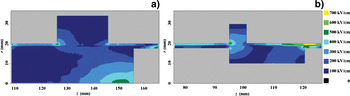
As the design and analysis mentioned above, the structure of the coaxial RBWO shown in Figure 1 should be improved to be that shown in Figure 13. Because the anode foil equipotentially connecting the inner and outer conductors is replaced by the resonant reflector, we adopt the equipotential support with six axisymmetric thin slices described in Figure 14, which will not interrupt the transmission of the electron beam. The equipotential support is designed and optimized carefully so that its microwave transmission coefficient of the quasi-TEM mode is high enough as shown in Figure 15a and the electromagnetic field can propagate through it with little reflection. Besides, according to our analysis, the maximum of the electric field amplitude in the equipotential support is a relative safe value, about 545 kV/cm as shown in Figure 15b.
Improved structure of coaxial RBWO. (1) annular cathode; (2) resonant reflector; (3) guide magnet solenoid; (4) outer SWS; (5) inner SWS; (6) fluting electron collector; (7) equipotential support; (8) output waveguide.

(Color online) Close-up view of equipotential support in Figure 13.

(Color online) (a) Microwave transmission coefficient of quasi-TEM mode of equipotential support. (b) Amplitude distribution of electric field in equipotential support in the case of 1 GW.

Driven by the pulsed power (Kovalchuk et al., Reference Kovalchuk, Kharlou, Zherlitsyn, Kumpjak, Tsoy, Vizir and Smorudov2009; Liu et al., Reference Liu, Yin, Ge, Zhan, Chen, Feng, Shu, Zhang and Wang2007), the electron beam emitted from the dense cathode plasma is confined by the guide magnetic field and is injected into SWS. The radial expansion of the cathode plasma will increase the beam diameter to scrape the resonant reflector. In the experiment, the radial expansion velocity of the cathode plasma is less than vpr = 1 cm/μs with the guide magnetic field higher than 1 T (Kovalev et al., Reference Kovalev, Nechaev, Petelin and Zaitsev1998). So the radial distance between the radius of the resonant reflector and the beam radius should be more than vprτb ≈ 1 mm, where τb is the electron beam pulse duration.
The bombardment of the spent electron onto the beam collector at the end of the coaxial SWS may lead to the secondary-emission multiplication and then the consequent plasma generation (Polevin et al., Reference Polevin, Korovin, Kovalchuk, Karlik, Kurkan, Ozur, Pegel, Proskurovsky, Sukhov and Volkov2004).When the electron beam dumps onto a clean collector surface at front surface doses exceeding about 100 J/g, plasma will be generated and stream back along the magnetic field lines into the microwave generation region (Benford & Benford, Reference Benford and Benford1997). In Figure 13, the electron collector is modified into a fluting one by notching the annular groove on the surface where the electron is bombarding. This structure of the electron collector is motivated by the form of the coaxial extractor (Liu et al., Reference Liu, Chen and Zhang2001). We make use of this fluting electron collector to prevent the plasma generated by the electron bombardment from expanding into SWS.
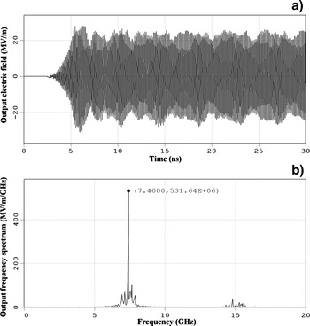
The results of the numerical simulation on the improved structure shown in Figure 13 are presented in Figure 16. The microwave pulse of 751 MW at 7.40 GHz is generated under the diode voltage 507 kV and current 3.99 kA. The guide magnetic field of 3.2 T is applied. The output efficiency is 37%, which is in agreement with the theoretical predication, 38% (Teng et al., Reference Teng, Xaio, Song, Sun, Chen, Shao and Liu2012).
Numerical simulation of coaxial RBWO. (a) Output electric field; (b) output frequency.

The scalar distribution of the electric field in the coaxial RBWO is analyzed in Figure 17a. The electromagnetic field in the coaxial RBWO is the superimposed field of the forward wave and the backward wave. In terms of the output power 1.0 GW the maximum electric field about 1.3 MV/cm, which is considered as the dangerous value capable of inducing explosive field electron emission, occurs on the sixth inner ripple as indicated in Figure 17b.
(Color online) Scalar distribution of the electric field in coaxial RBWO in terms of the output power 1.0 GW.

Surface Treatment
In order to raise the breakdown threshold and lower the secondary electron emission yield, the coaxial RBWO are suggested to be carefully surface-treated by several steps. First the important components should be electrochemically polished to remove the microscopic bumps and spires on the metallic surfaces, which can enhance electric fields by a factor of 100 or even 1000 (Benford & Benford, Reference Benford and Benford1997). Then the tube should be baked in vacuum furnace to disrobe the oil and gas molecules from the metallic surfaces, especially the water molecules and the hydrogen atoms (Gilgenbach et al., Reference Gilgenbach, Hochman, Jaynes, Cohen, Rintamaki, Peters, Vollers, Lau and Spencer1998). Finally, the TiN film with the thickness of 100 nm, which makes the metallic surface have a low secondary electron emission yield, is evaporated onto the stainless steel surface (Mayberry et al., Reference Mayberry, Wroblewski, Schamiloglu and Fleddermann1994; Polevin et al., Reference Polevin, Korovin, Kovalchuk, Karlik, Kurkan, Ozur, Pegel, Proskurovsky, Sukhov and Volkov2004).
EXEPERIMENT RESEARCH
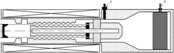
The experiment research on the coaxial RBWO is performed on the accelerator SINUS-881, which can produce the electron beam pulse of the full width at half maximum (FWHM) 28 ns. In our experiment, the output power of the coaxial RBWO is measured by the electric probe mounted on the output waveguide and validated by the calorimeter simultaneously for each shot as shown in Figure 18. The total experiment system can be evacuated by turbo-molecular pump up to 10−3 Pa, which is in favor of the elimination of the pulse shortening (Korovin, Reference Korovin1999). Besides, the important components such as the insulator, the cathode shank and the calorimeter are carefully washed and cleaned or baked to make sure the cleanness of the experiment system. Before the experiment, the coaxial RBWO should be conditioning through repeated operating. The structures of the coaxial RBWO shown in Figure 1 and Figure 13 are compared in our experiment.
Scheme of the measurement in our experiment. The output power of the coaxial RBWO is measured by the electric probe 1 mounted on the output waveguide and validated by the calorimeter 2 simultaneously for each shot in order to make sure the experiment result is accurate.

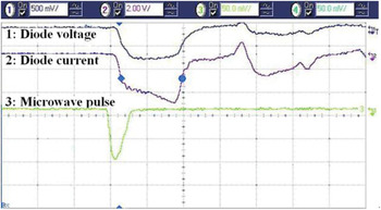
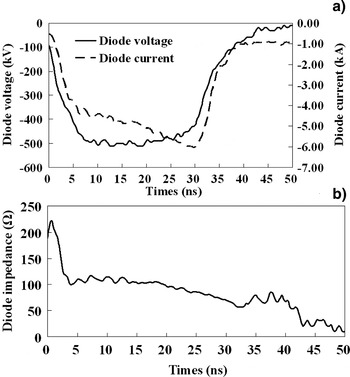
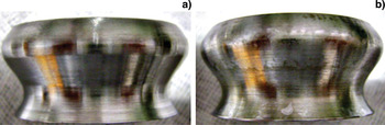
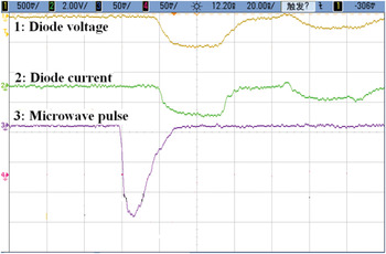
Our previous experiment is performed with the structure shown in Figure 1, which was predicted to achieve the output efficiency higher than 37% (Liu, Reference Liu2002) by numerical simulation. But in experiment its typical generated waveform in Figure 19 shows the great difference from the numerical simulation result. Under the diode voltage 511 kV and current 4.96 kA, the output power no more than 460 MW and the efficiency less than 20% are obtained with the guide magnetic field 3.2 T after conditioning through repeated operating. The microwave pulse duration is about 8 ns, much less than that of the electron beam. In Figure 19, the diode current increases remarkably while the diode voltage maintains the constant. As a result, the diode impedance falls rapidly with times as described in Figuree 20, in which the impedance decreases from 116 Ω to 67 Ω during the flat stage of the diode voltage from 8 ns to 30 ns. This time-dependent variation of the diode current remarked by impedance collapse results from the decrease of the cathode gap by the plasma generated from the anode foil during the transmission of the electron beam. It can be deduced that the transmission of the electron beam is terribly interrupted, which is responsible for the both of the pulse shortening and the low output power and efficiency. After experiment, the surface conditions of every component of the coaxial RBWO are carefully investigated. The most impressive result demonstrated in Figure 21 indicates that the traces marked by the explosive field electron emission and the secondary electron bombardment on the sixth ripple are much heavier than those on the first one. These results agree with the analysis of the electric field illustrated in Figure 17 very well. From Figure 20 and Figure 21 it can be concluded that the interruption of the beam transmission and the combining effects of the explosive field electron emission and the secondary electron multipactor are the main causes for the pulse shortening in the coaxial RBWO.
(Color online) Typical experiment results of the structure shown in Figure 1. The resolution is 20 ns/div on the horizontal axis. (1) diode voltage, 511 kV; (2) diode current, 4.96 kA; (3) microwave pulse, 456 MW.


(Color online) Comparison between the surface conditions of the first and sixth inner ripples after experiment. (a) The first ripple. (b) The sixth ripple.

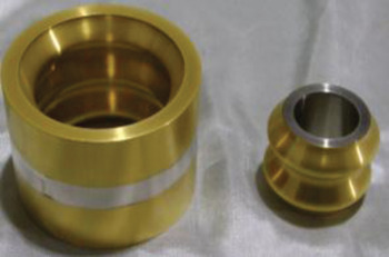
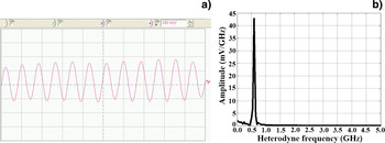
The further experiment research focuses on the structure of the coaxial RBWO shown in Figure 13. Besides a series of modification and improvement on the diode structure, SWS optimization and the collector design proposed by our physical design and analysis, the coaxial RBWO is surface-treated carefully as shown Figure 22. After conditioning through repeated operating the microwave pulses with the output power higher than 730 MW and the pulse duration about 20 ns are generated under the diode voltage 500 kV and current 4.3 kA with the guide magnetic field 3.2 T as shown in Figure 23. The output efficiency is about 34%, and the output frequency measured by the heterodyne method is 7.4 GHz as shown in Figure 24, which are close to the simulation prediction. It is found that in Figure 23 after reaching the steady state the diode current maintains the constant as the diode voltage does with little impedance collapse appearing. This is corresponding to the replacement of the anode foil by the resonant reflector. The electron beam can travel through SWS and interacts with the electromagnetic field without any interruption. Besides, the surface treatment raises the breakdown threshold and lowers the secondary electron emission yield. As a result, the output efficiency and the pulse duration shown in Figure 23 are greatly increased compared to those in Figure 19.
(Color online) Outer and inner ripples coated with the TiN film.

(Color online) Typical experiment results of the structure shown in Figure 13. The resolution is 20 ns/div on the horizontal axis. (1) diode voltage, 505 kV; (2) diode current, 4.26 kA; (3) microwave pulse, 733 MW.

(Color online) (a) Waveform derived from heterodyne method. Local frequency is 8.0 GHz. (b) FFT of heterodyne signal.

When the diode voltage rises to 560 kV, the output power and efficiency increase up to 1.01 GW and 36%, but the pulse duration, about 16 ns, starts to present the form of pulse shortening as described in Fig. 25. However, compared to that in Fig. 19, the diode current in Fig. 25 does not increase with time on the steady state, which indicates that the diode impedance does not collapse in this case. Therefore, the pulse shortening under the diode voltage 560 kV results from the combining effects of the explosive field electron emission and the secondary electron multipactor on the surface. And it can be concluded that the breakdown threshold on the treated stainless steel surface at 7.4 GHz in the coaxial RBWO is 1.2 MV/cm.
(Color online) Typical experiment results of the structure shown in Figure 13 under the increased diode voltage. The resolution is 20 ns/div on the horizontal axis. (1) diode voltage, 561 kV; (2) diode current, 5.03 kA; (3) microwave pulse, 1.01 GW.

DISCUSSION
As a new type of the HPM source device with high output efficiency, the coaxial RBWO encounters the more serious problem of the pulse shortening due to its special coaxial structure. Our study has found that in the coaxial RBWO, the two main reasons responsible for the pulse shortening are the interruption of the beam transmission and the combining effects of the explosive field electron emission and the secondary electron multipactor on the surface. The researches on the electrodynamic structure presented in this paper have provided an effective method to avoid the beam interruption. The structure optimization including the diode region, SWS and the electron collector and the series of surface treatment are proved to be practical to avoid the surface breakdown and depress the generation of the unexpected plasma. It is found that when the diode voltage rises from 500 kV to 560 kV, although the phenomenon of pulse shortening happens due to the explosive field electron emission and the secondary electron multipactor, the output power and efficiency are increased. Therefore it can be expected that if the limitation of the breakdown and pulse shortening is eliminated, the output power and the efficiency of the coaxial RBWO can be enhanced further even by taking advantage of the resonant reflector suggested in Fig. 8 (b).