Introduction
Bandpass filters are basic components in RF and microwave systems providing little insertion loss in the passband and huge suppression in the stopband. To accommodate multiple services or standards, multi-band bandpass filters are necessary at such request. There are several promising dual-band bandpass filter designs suitable for the competition [Reference Tsai and Huse1–Reference Quendo, Rius and Person10]. In [Reference Tsai and Huse1], a synthesizing method is presented to design a microwave dual-band filter consisting of a bandstop filter and a wide-band bandpass filter in a cascade topology. By tuning the frequency ratio of the first two resonant modes, stepped-impedance resonators are used to realize dual-band bandpass filters [Reference Chen, Huang and Wu2, Reference Sun and Zhu3]. Stub-loaded resonators can also adjust the frequency ratio of the first two resonant modes and are employed to design dual-band bandpass filters [Reference Zhang, Chen, Xue and Li4, Reference Mondal and Mandal5]. In [Reference Chen and Hsu6], two single-band bandpass filters are integrated into a dual-band bandpass filter with two long feeding lines. The multilayer structure is a good solution to shrink area for compact dual-band bandpass filters [Reference Wu, Chen and Chen7–Reference Joshi and Chappell9]. In [Reference Quendo, Rius and Person10], three open-circuited stubs in parallel are introduced to implement three transmission zeros for separating the two passbands.
Considering limited preparation time, ease of in-house fabrication, and tuning after fabrication, three viable topologies are investigated and compared. The first bandpass filter utilizes stepped-impedance resonators. Common input and output resonators are used to reduce size. To increase selectivity and design freedom, a three-pole topology is used, where the two passbands do not share the middle resonators. The second bandpass filter utilizes parallel coupling technology and two half-wavelength resonators each loaded with an open-circuited stub in the middle. Each resonator is a dual-mode resonator, and each passband goes through their respective path achieving high design freedom and a low loading effect. The third filter is similar to the second one. However, two half-wavelength resonators loaded with short-circuited stub in the middle are used for compact size. Also, a lumped surface-mounted capacitor is soldered between the input and output feeding lines to generate enough cross-coupling for creating transmission zeros beside the passbands to achieve a good selectivity.
Dual-mode resonators
The final filter is evaluated by the following figure of merit (FoM), where a low value is favorable.

The first passband frequency is from 900 to 1000 MHz and the second passband frequency is from 1427 to 1518 MHz. |S 21(900 MHz)| is the absolute value of the measured S 21 parameter in dB at 900 MHz, and A is the surface area in mm2. The rejection is defined as the worst value of |S 21| for frequencies within the specified stopbands. To obtain a small FoM, the final filter must achieve compact size, low insertion loss, high rejection, and good selectivity. Resonators are major building blocks for a bandpass filter. A resonator with the first two controllable resonant frequencies is crucial for a single-band bandpass filter design and a dual-band bandpass filter design. The two resonant modes can be close to each other for a single-band operation. On the other hand, when the two resonant modes are apart, two of such resonator can realize a two-pole dual-band bandpass filter. There are three resonators under evaluation. Each has advantages and disadvantages. Together with feeding technology, the bandpass filters are realized and compared using the FoM.
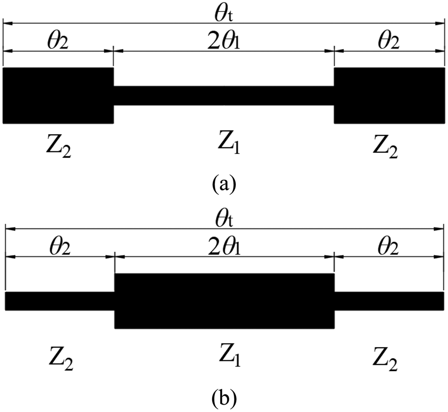
Figure 1 shows two types of the stepped-impedance resonator in microstrip technology. The even- and odd-mode resonant condition can be derived as [Reference Makimoto and Yamashita11]


where the impedance ratio K = Z 2/Z 1 and the electrical length ratio α = θ 2/(θ 1 + θ 2) = θ 2/θ t. When K = 1, it is a uniform-impedance resonator, and the frequency ratio of the second and the first resonant frequencies is 2. When K < 1 as shown in Fig. 1(a), the frequency ratio is greater than two. When K > 1 as shown in Fig. 1(b), the frequency ratio is less than two. Also, the electrical length ratio can be tuned for a wider variety of frequency ratio. However, such resonator is impractical for frequency ratio very close to one, and it is not useful for narrow-band, dual-mode, and single-band bandpass filter. Nevertheless, in a dual-band bandpass filter with a proper frequency ratio, if the stepped-impedance resonators are used as common resonators, the resonator number can reduce and the circuit would be compact.
Stepped-impedance resonators in microstrip technology. (a) K < 1 (b) K > 1.

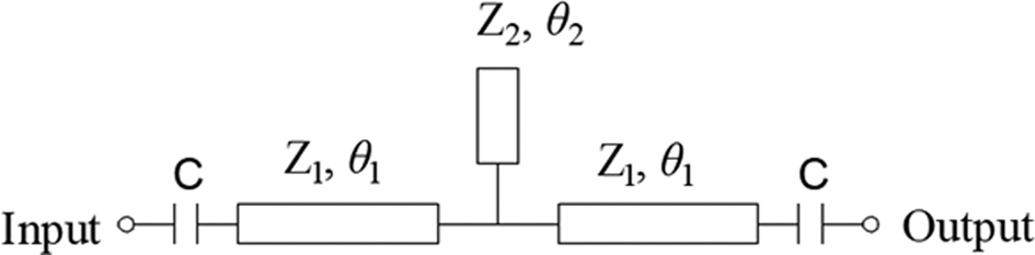
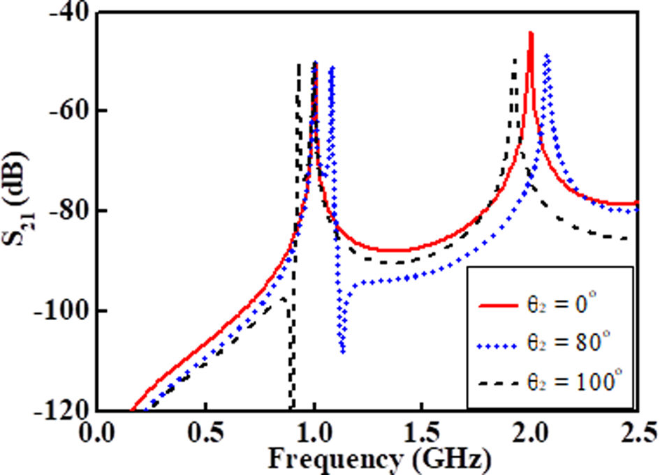
Figure 2 shows a half-wavelength resonator with a shunt open-circuited stub in the middle [Reference Tu, Li, Michalski and Chang12]. In order to investigate the resonant frequency, the resonator is loosely coupled via two 10-fF capacitors. The electrical length θ 1 is 90o at 1 GHz, and Z 1 = Z 2 = 50 for simplicity. Figure 3 shows the resonant mode analysis with different stub electrical length θ 2. The first odd mode is at 1 GHz and is determined by the electrical length θ 1. When θ 2 is 80o, the first even mode frequency is at 1.08 GHz. There is a transmission zero at 1 (GHz) × 90/80 = 1.125 GHz. When θ 2 is 100°, the first even mode frequency is 0.93 GHz. There is a transmission zero at 1 (GHz) × 90/100 = 0.9 GHz. It should be noted that the first odd mode is fixed when θ 2 is tuned. The first even mode frequency could be easily tuned above or under the first odd mode frequency. If one resonator is used, such resonator can be used for dual-mode single-band bandpass filter design. The bandwidth can be easily adjusted with different shunt stub lengths.
A loosely coupled-resonator with shunt open-circuited stub.

Resonant mode analysis with different θ 2 = 0°, 80°, and 100°.

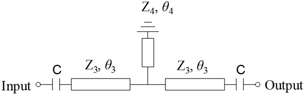
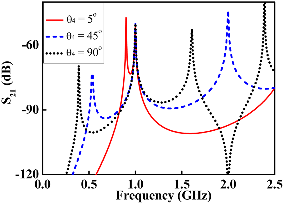
Figure 4 shows a half-wavelength resonator loaded with a short-circuited stub in the middle [Reference Zhou, Tang and Xiao13], and the resonator is loosely coupled via two 10-fF capacitors for mode analysis. The electrical length θ 3 is 90° at 1 GHz, and Z 3 = Z 4 = 50 for simplicity. Figure 5 shows the resonant mode analysis. The first odd mode frequency is fixed at 1 GHz for different stub electrical length θ 4. The first even mode frequency is always lower than 1 GHz, and increases as θ 4 decreases. Again, such resonator can be used for dual-mode single-band bandpass filter design. The bandwidth can be easily tuned with different shunt stub length. In comparison to the resonator with an open-circuited stub, although there is no transmission zero near the passband for better selectivity, the shorter stub saves circuit size.
A loosely coupled-resonator with shunt short-circuited stub.

Resonant mode analysis with different θ 4 = 5°, 45°, and 90°.

Dual-band bandpass filter designs
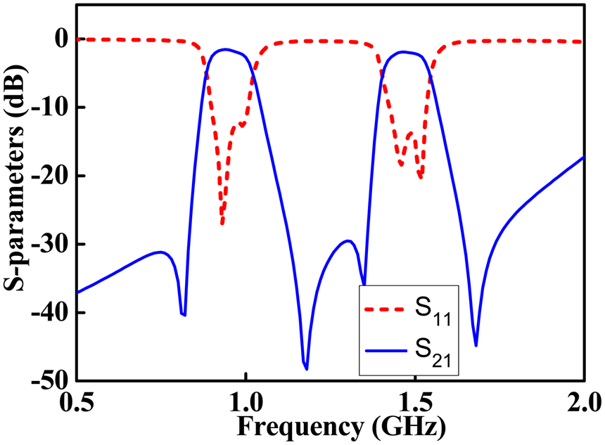
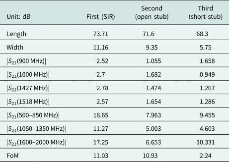
Figure 6 shows a three-pole dual-band bandpass filter using stepped-impedance resonators. The center frequency (fractional bandwidth) for band 1 and band 2 is 0.95 GHz (10.5%) and 1.47 GHz (6.2%), respectively. The filter is of 0.1-dB ripple Chebyshev response. The design procedure for a single-band bandpass filter can be found in [Reference Hong and Lancaster14]. Common input and output resonators resonate at both passband frequencies for a compact size. The left-center stepped-impedance resonator is for band 1, and the right-center uniform-impedance resonator is for band 2. Ideally, a compact two-pole structure is a better solution. However, the required coupling coefficients are difficult to simultaneously match for both bands with little design freedom. Hence, the two center resonators are introduced. Since each resonator is for a respective band, it is easy to optimize the coupling coefficients. The required external quality factor (coupling coefficient) for band 1 and band 2 is 9.82(0.097) and 16.64(0.057), respectively. Two tapped feeding lines are connected to the two common resonators. Conventionally, the tapping position is adjusted to match the external quality factors. However, in the dual-band operation, the microstrip line impedances must be tuned as the impedance ratio is fixed. The first filter is simulated with a 0.635-mm RT/Duroid 6010LM substrate. The dielectric constant is 10.2 and the loss tangent is 0.0023. The dimensions are L 1 = 28.27, L 2 = 22.72, L 3 = 23.37, L 4 = 11.37, L 5 = 41.5, W 1 = 1.04, W 2 = 0.19, W 3 = W 5 = 0.3, W 4 = 1.25, G 1 = 0.305, G 2 = 0.64, all units in mm. Figure 7 shows the simulated results. The simulated insertion loss at 900/1000/1427/1518 MHz is 2.52/2.7/2.78/2.57 dB. The worst rejection in 500 − 850 /1050 − 1350 /1600 − 2000 MHz are 18.65/11.27/17.25 dB. The circuit size is 73.71 × 11.16 mm2 and all of these correspond to a FoM of 11.03.
The three-pole dual-band bandpass filter using stepped-impedance resonators.

The simulated results for the dual-band bandpass filter using stepped-impedance resonators.

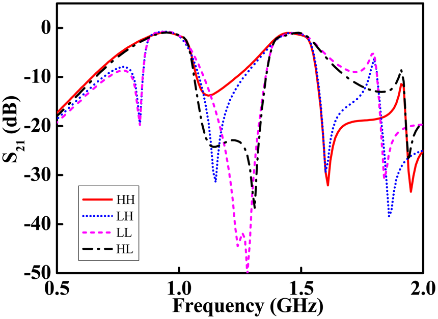
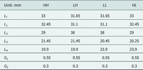
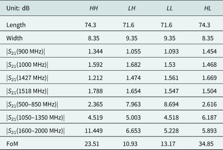
Figure 8 shows the dual-band bandpass filter using resonators with the loaded open-circuited stub. The two narrow feeding lines are parallel coupled to the two resonators. The two shunt stubs are bent for a compact size. The upper resonator is for band 1, and the lower one is for band 2. The two gaps G 1 and G 2 between the feeding lines and the resonators are the main parameters tuned for the required external quality factors. The mutual coupling between the two resonators is low, and the performance of each band can be optimized independently. Since the resonator is inherited with one transmission zero, there are four possible arrangements for such filter, where HH is the case with both transmission zeros at respective high stopband, and LL is the case with both transmission zeros at respective low stopband. The second filter is simulated with a 1.27-mm RT/Duroid 6010LM substrate. A thick substrate is used for more coupling between the feeding line and resonator. The dimensions for the four cases are listed in Table 1, and all the line width is 0.3 mm. Figure 9 shows the simulated S 21 of the four cases. Their performance is summarized in Table 2. It shows that the LH case achieves the best FoM of 10.93, where a transmission zero is at the low band of band 1 and a transmission zero is at the high band of band 2.
The two-pole dual-band bandpass filter using resonators with a loaded open-circuited stub.

The simulated results for the dual-band bandpass filter using resonators with a loaded open-circuited stub.

The dimensions of the four cases of the second filter

The simulated results of the second filter

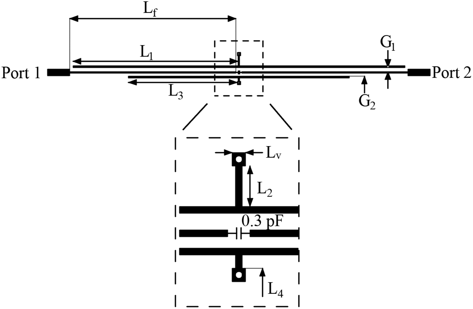
Figure 10 shows the dual-band bandpass filter using resonators with the loaded short-circuited stub. Short-circuited stubs are used to replace the open-circuited stubs for a compact size. The detailed design procedure is as follows.
1. Design two single-band bandpass filters.
2. Set center frequency = 0.95/1.47 GHz, fractional bandwidth = 10.5%/6.2%, lowpass frequency prototype = both are 0.1-dB Chebyshev response.
3. Adjust resonators' parameters: the two-mode frequencies for band 1 is 0.909 GHz/0.983 GHz, and those for band 2 is 1.434 GHz/1.5 GHz [Reference Hong and Lancaster14]. The half-wavelength resonators resonate at 0.983 GHz or 1.5 GHz. Adjust stub lengths such that the resonators also resonate at 0.909 GHz or 1.434 GHz.
4. Adjust G 1 and G 2 such that the required external factors of 8 or 13.6 are satisfied.
5. Integrate the two single-band filter in a parallel configuration. The loading effect is low and only slight final optimization is needed.
The two-pole dual-band bandpass filter using resonators with a loaded short-circuited stub.

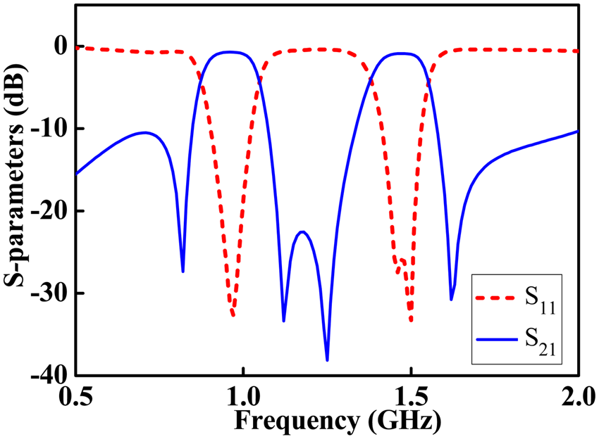
The via hole diameter is 0.3 mm. In such configuration, cross-coupling generates two transmission zeros near each passband [Reference Tu15]. A 0.3-pF lumped capacitor between two feeding lines is used for enhancing coupling, and the transmission zeros frequency can move toward passbands for a sharp rejection. The third filter is simulated with a 1.27-mm RT/Duroid 6010LM substrate. The dimensions are Lf = 30 mm, L 1 = 29.45 mm, L 2 = 1.8 mm, L 3 = 19.55 mm, L 4 = 0.6 mm, Lv = 0.6 mm, G 1 = 0.75 mm, and G 2 = 0.5 mm. The line width is 0.3 mm. Figure 11 shows the simulated results. The simulated insertion loss at 900/1000/1427/1518 MHz is 1.658/0.949/1.267/1.286 dB. The worst rejection in 500 − 850/050 − 1350/1600 − 2000 MHz are 9.455/4.603/10.331 dB. The circuit size is 68.3 × 5.75 mm2 and all of these correspond to a FoM of 2.24. The comparison Table 3 lists the simulated performance of the three circuits. For the first filter, it is a 3-pole filter, and the high stopband rejection is obtained at the cost of high in-band insertion loss. For the second filter, the open-circuited stubs occupy a large area. For the third filter, it achieves the smallest size, fair insertion loss, and fair rejection. All of these make it achieve the smallest FoM among the three. Figure 12 shows the final fabricated filter. The measured insertion loss at 900/1000/1427/1518 MHz is 1.053/1.504/1.233/1.231 dB. The worst rejection in 500 − 850/1050 − 1350 /1600 − 2000 MHz are 4.117/6.218/10.606 dB. The measured FoM of the final filter is 3.48.
The simulated results for the dual-band bandpass filter using resonators with a loaded short-circuited stub.

The final filter (a) photograph (b) simulated and measured results.

Simulated performance comparison

Conclusion
Given the FoM of a dual-band bandpass filter, three topologies are investigated for optimal size, insertion loss, and rejection. Also, high design freedom and ease of tuning after fabrication are necessary due to the limited preparation time. With parallel coupling technology for a low loading effect between two channels, two resonators with loaded short-circuited stub for a compact size, and a lumped capacitor to enhance cross-coupling resulting a sharp rejection, an optimal design is implemented with a measured FoM of 3.48.
Acknowledgements
This work was supported in part by the Ministry of Science and Technology, Taiwan, under contract no. MOST 107-2221-E-008-059.
 Wei-Chung Chang received the B.S. degree in electrical engineering from National Taiwan Ocean University, Keelung, Taiwan, R.O.C., in 2018, and is currently working toward the M.S. degree in electrical engineering at National Central University, Taiwan. His research interests are microwave passive circuits, mainly filters and multiplexers.
 Wen-Hua Tu received the B.S. degree in communication engineering from National Chiao Tung University, Hsinchu, Taiwan, R.O.C., in 1999, the M.S. degree in communication engineering from National Taiwan University, Taipei, Taiwan, R.O.C., in 2001, and the Ph.D. degree in electrical engineering from Texas A&M University, College Station, TX, USA in 2006. From 2003 to 2006, he was a Research Assistant with the Electromagnetics and Microwave Laboratory, Texas A&M University. In 2007, he joined the Department of Electrical Engineering, National Central University, Taiwan, as an Assistant Professor, and is now a Professor. He has authored or coauthored over 80 papers in the areas of antennas and microwave passive components. Dr. Tu is a member of The Honor Society of Phi Kappa Phi, and he received the 2007 AP-S Graduate Research Award.