Introduction
The original design of dye-sensitized solar cells (DSSCs) is typically constructed from a thick film of TiO2 nanoparticles, which is sintered into a mesoporous network with a large internal surface area for the maximum adsorption of light-harvesting dye molecules.[Reference O'regan and Grätzel1] Upon illumination, the sensitizer dye-excited states undergo rapid charge separation, with electrons injected into the nanocrystalline TiO2 film and holes exiting the cell by means of redox species in a liquid or solid-state electrolyte. Electron transport is one of the prominent processes in the cell and is of major importance for the overall performance of the device. Electron transport is a complex process because the transport medium is a mesoporous film, and the gaps in the pores are completely filled by the electrolyte with high ionic strength, resulting in electron–ion interactions. Therefore, the electron transport in these so-called state-of-the-art systems has a practical limit in terms of improving the DSSCs efficiency because of the low electron diffusion coefficient in this randomly oriented mesoporous film photoanode.[Reference Kopidakis, Benkstein, van de Lagemaat and Frank2] Although some DSSC cells operate with high electron transport efficiency, ultimately cell performance is constrained by a balance between light path length and electron transport limitations. Improvements in the device performance could be possible by optimizing the conduction path and transporting the electrons as quickly as possible to avoid recombination of the charge carriers. Several approaches have been reported in the literature, which focus on achieving the above strategy. One-dimensional (1D) nanowires were used to construct efficient DSSCs. Advanced DSSCs have been reported in which the photoanode consists of ZnO and TiO2 nanowire, nanorod, and nanotube structures synthesized by chemical or physical methods[Reference Zukalova, Zukal, Kavan, Nazeeruddin, Liska and Grätzel3] or ZnO–ZnO core–shell nanowire arrays for blocking recombination.[Reference Guillen, Azaceta, Vega-Poot, Idigoras, Echeberria, Anta and Tena-Zaera4] Examples include preparation of hybrid structures by introducing hydrothermal anatase TiO2 nanotubes into TiO2 films,[Reference Wu, Chen, Lu, Wu and Chen5] growing ZnO nanowires in a liquid medium, or by metal organic vapor phase epitaxy,[Reference Law, Greene, Johnson, Saykally and Yang6–Reference Baxter and Aydil8] making TiO2 nanorods by using an electrospinning method,[Reference Song, Ahn, Jo, Kim and Ahn9] and anodic oxidation of titanium metal plates to form TiO2 nanotubes.[Reference Wang, Yip, Cheung, Djurisic, Xie, Leung and Chan10–Reference Stergiopoulos, Ghicov, Likodimos, Tsoukleris, Kunze, Schmuki and Falaras12] The large nanocrystallite surface area available for dye adsorption in nanotube photoanodes leads to efficient light harvesting. Also, the nanotubes provide an easier pathway to capture photogenerated charges where the electron transport direction is parallel to the nanotube orientation.[Reference Kamat13] However, the need for decreasing the recombination of electrons and holes after band gap excitation was not fulfilled due to the bulk defects and grain boundaries, which are the major causes of limited photoconversion efficiency.[Reference Wang, Huang, Cao, Yu, Deng, Liu, Huang, Huang, Huang, Guo and Liang14] Also, the work focusing on 1D nanostructure involved the oxide layer available for dye adsorption, while the interface between the fluorine-doped tin oxide (FTO) glass electrode and the oxide layer was still flat. The cell performance can be improved if the area of this second interface is maximized, which could increase the rate of charge capture. Three-dimensional (3D) core–shell structures having TiO2 as shell and various metals or metal oxides as core via electrodeposition have been reported.[Reference Xie, Zhou, Huang, Huang and Lu15–Reference Feng, Ji, Duan, Zhu, Jiang, Ding, Meng, Ding, Liu, Hu and Huang24] We have recently reported the successful application of Au–TiO2 core–shell nanowire arrays as photoanode materials in advanced 3D DSSCs using two different approaches.[Reference Sahu, Gordon and Tarr25, Reference Sahu, Wang, Gordon, Zhou and Tarr26] In our reported methods, dye desorption experiments showed the similar dye loading among all devices tested (nanowire array photoanodes and mesoporous film photoanodes). Consequently, changes in dye loading could not account for the enhanced efficiency of the core–shell devices. Likely explanations include: (1) improved electron transport due to the presence of the conducting metal core within the ~20 nm TiO2 film compare with the ~15 µm thick mesoporous TiO2 nanoparticle film where electrons need to transfer from particle to particle to reach the transparent conductive oxide, (2) increased effective path length of the entering photons due to scattering from the metal nanowire arrays, and (3) enhanced absorbance caused by optical effects of the metal nanowire array such as enhanced localized surface plasmon resonance. Upon excitation the free electrons in gold cause large near-field amplitude and a resonantly enhanced scattering cross-section known as near field scattering. If the large near field in the vicinity of the gold nanostructure would be overlapped by the extinction of the light-absorbing material such as the dye of the solar cell, the overall absorption by the dye will be increased. As a result, the plasmon-enhanced absorbance of the dye would increase due to the increased electromagnetic field. Such localized fields can excite the dye more efficiently than the incident light, so the gold nanowire arrays may function as light-harvesting antennas for the dye molecules as long as the dye molecules are near the metal's effective electromagnetic field.
The 3D core–shell Au–TiO2 nanowire arrays showed improved photovoltaic performance because of the greatly increased interface area, efficient charge separation, ease of transport, and light-focusing effects (scattering and/or localized surface plasmon resonance). However, gold is a relatively expensive metal, potentially limiting its applicability in these advanced 3D core–shell devices. In this study, the versatile method was carried out to fill the TiO2 nanotubes with a less expensive metal such as Ni. High-yield Ni–TiO2 core–shell nanowire arrays were prepared and applied as photoanodes in advanced DSSCs.
Experimental
Synthesis of TiO2 nanotubes
The TiO2 nanotubes were prepared similarly to those previously reported.[Reference Sahu, Gordon and Tarr25] Commercial anodic aluminum oxide (AAO) membranes (Whatman 13, 0.2 µm) were uniformly and conformally coated with titanium isopropoxide, Ti(OC3H7)4 mixed with ethanol. The weight ratio of Ti(OC3H7)4:C2H5OH was 3:1. The membrane was immersed in the precursor solution for 15 min, and then excess liquid was wiped off from the exposed surface of the membrane. The above process generated TiO2 nanotubes up to 15 µm long within the AAO template. Next, the sample was annealed at 500 °C for 30 min in air to achieve a highly crystalline anatase TiO2 phase. For SEM observation, the AAO template was removed by chemical etching using 3 M NaOH (aq) for 45 min, which produced highly aligned arrays of TiO2 nanotubes perpendicular to the substrate.
Synthesis of Ni–TiO2 core–shell nanowire arrays
After the TiO2 nanotubes were obtained with the desired anatase phase and morphology, bottom up room temperature constant current electrodeposition was carried out in order to grow Ni–TiO2 core–shell nanowire arrays. The same procedure was followed as described previously for synthesizing Au-TiO2 nanowire arrays.[Reference Sahu, Gordon and Tarr25] The nickel plating solution (nickel sulfamate RTU) was purchased from Technic, Inc. Electrodeposition was carried out using a single channel potentiostat (EG&G Instruments Model 263A). After preparing TiO2 nanotubes in an AAO template, one side of the template was sputtered with a thin film of Ag (~20 nm). The exposed silver was attached to copper tape and masked so that only the open pores of the template were exposed to the nickel-plating solution. Nanowire arrays were grown into the TiO2 nanotubes with a constant current of −0.9 mA for up to 30 min in the nickel plating solution. This deposition allowed the wires to grow as far as to the top of the nanotubes, filling the entire channel within the TiO2 tubes with Ni nanowires. After Ni deposition, the sample was rinsed with distilled water, and the AAO was etched slowly away with 3 M NaOH (aq) for 45 min. The obtained core–shell nanowire arrays were washed several times with distilled water resulting in well-aligned nanowire arrays on a copper substrate. The nanowire arrays were later removed from the copper tape by washing with acetone and transferred to an FTO substrate (Solaronix, TCO10-10, sheet resistance 10 Ω/sq).
Preparation of mesoporous TiO2 nanoparticle film on FTO
The mesoporous anatase TiO2 film used as photoanode for comparison with the core–shell photoanodes was prepared as previously reported.[Reference Lee, Hwang, Guo, Ho, Buchholtz, Wang and Chang27] The prepared TiO2 paste was spread on an FTO substrate by doctor-blade technique to give a uniform flat and smooth surface using an adhesive tape spacer. The thickness of the nanoparticles film was measured using a profilometer (SLOAN Dektak II).
Characterization
The structures were characterized by a Carl Zeiss 1530 VP field emission scanning electron microscope (FESEM). The compositional analysis was conducted by energy dispersive x-ray spectroscopy (EDS). For x-ray diffraction (XRD), TiO2 nanotube samples were attached to a glass substrate using epoxy glue. The XRD patterns of samples were collected by a Philips X-pert PW 3040 MPD x-ray powder diffractometer operated at 40 kV and 40 mA current with Cu Kα radiation.
Structural characterization and phase determination of TiO2 nanotubes
The FESEM image and the XRD data of synthesized nanotubes are given in Fig. 1, which shows that the synthesized structures were clearly composed of well-aligned TiO2 nanotube arrays. The TiO2 nanotubes were ~5 µm in length with a ~200 nm outer diameter. A large-scale FESEM image of well-aligned TiO2 nanotube arrays has been given in supporting information Fig. S1(a). The XRD pattern confirmed the highly crystalline anatase phase of the as synthesized TiO2 nanotubes. The XRD pattern contained several peaks corresponding to anatase, and the absence of a peak at 27.45° (rutile) suggests that the nanotubes consist predominantly of crystalline anatase TiO2 phase.
(a) SEM of TiO2 nanotubes and (b) XRD data from the nanotube array.

Structural characterization of Ni–TiO2 core–shell nanowire arrays
After preparation of the nanowire arrays, the structures were characterized both morphologically and compositionally, as shown in Fig. 2. Figures 2(a)–2(c) represent the cross-section and top views of the Ni-filled TiO2 nanotubes taken at various magnifications by FESEM. The images prove the successful growth of the Ni–TiO2 core–shell nanoarchitectures. A large-scale FESEM image of top view, uniform Ni–TiO2 core–shell nanowire arrays has been given in supporting information Fig. S1(b). Figure 2(d) presents the EDS data for the Ni–TiO2 core–shell nanowire arrays, which clearly indicate the presence of Ni, Ti, and O in the spectrum.
FESEM images of Ni–TiO2 core–shell nanowire arrays (a)–(c) and corresponding EDS data (d).
Solar cell fabrication and electrochemical characterization
Photoanodes utilizing TiO2 nanotube and Ni–TiO2 nanowire arrays were prepared by transferring the nanostructures onto a FTO glass substrate obtained from Solaronix (TCO10-10, sheet resistance 10 Ω/sq) using our previously reported method[Reference Sahu, Gordon and Tarr25] as depicted in Fig. 3. In detail, the AAO containing TiO2 nanotubes or Ni–TiO2 core–shell nanowires were dissolved in 3 M NaOH, which resulted in free arrays of TiO2 nanotubes or Ni–TiO2 core–shell nanowires in NaOH solution. The arrays of nanotubes or Ni–TiO2 nanowires were washed with DI H2O four times in order to remove the residual NaOH. The nanostructures were then washed with ethanol to remove residual water. The freely suspended nanostructure arrays were then transferred and adhered onto a pre-cleaned FTO slide and annealed in air at 450 °C for 30 min. The resulting TiO2 nanotube or Ni–TiO2 core–shell nanowire film on the FTO was sensitized with dye (N-535, Solaronix) solution overnight. The same procedure was used for the fabrication of frontside (anode) illuminated devices as was done for the Au–TiO2 core–shell nanowire cells described previously.[Reference Sahu, Gordon and Tarr25] Additional devices were fabricated using mesoporous TiO2 nanoparticle film-based photoanodes for comparative studies. Photovoltaic data were measured using a 150 W xenon lamp solar simulator (Newport 96000) that was fitted with an Air Mass 1.5 filter (Newport 81094). The light intensity of the xenon light source was adjusted to 100 mW/cm2 using an NREL calibrated silicon photodiode (Hamamatsu S1787-08 for visible to IR range). J–V data were generated using a Keithley 2400 source meter. The J–V characteristics were measured under 1 Sun (AM 1.5 G, 100 mW/cm2). The current–voltage characteristics of TiO2 nanotube solar cells were compared with that of Ni–TiO2 nanowire device and the corresponding TiCl4-treated cells.
Schematic of the method of transferring the Ni–TiO2 core–shell nanowire arrays onto FTO and solar cell fabrication.
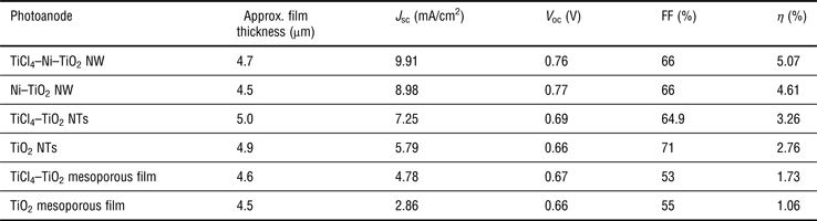
The comparative J–V characteristic studies of DSSCs with and without TiCl4 treatment are plotted in Fig. 4. The average length of each photoanode film (nanotube, nanowire, or mesoporous film) was in the range of 4.5–5.0 µm. Without TiCl4 treatment, the TiO2 nanotube based DSSC yielded an overall power conversion efficiency (η) of 2.76%, whereas the power conversion efficiency was increased to 3.26% with a short-circuit current density (J sc) of 7.25 mA/cm2, open circuit voltage (V oc) of 0.69 V, and fill factor (FF) of 64.9% after the surface treatment with TiCl4. By employing the reductively electrodeposited Ni–TiO2 core–shell nanowire, the DSSC showed enhanced photoconversion efficiency (η = 4.61%) with increased V oc, J sc and FF values (0.77 V, 8.98 mA/cm2 and 66%, respectively). The significantly enhanced efficiency after employing the Ni–TiO2 nanowire array is likely due to decreased charge transport resistance caused by the highly conductive Ni cores and by light path length enhancements resulting from the metal core. Furthermore, the TiCl4 treated Ni–TiO2 core–shell nanowire DSSC showed even higher performance in terms of conversion efficiency and current generation up to η = 5.07 % and 9.91 mA/cm2, respectively. The post-treatment of TiCl4 on Ni–TiO2 core–shell nanowire arrays, adds an extra layer of TiO2 onto the nanostructures constituting the film. Different explanations of the working principle of this coating have been reported in literature. These hypotheses concern increased surface area, improved electron transport, surface passivation, light scattering, TiO2 purity, and dye anchoring. Enhanced light scattering and surface passivation are likely the main reasons for the improved performances in our system. The FF remained the same, and open-circuit voltage was similar: V oc = 0.77 and 0.76 V for bare Ni–TiO2 nanowire and TiCl4–Ni–TiO2 nanowire devices, respectively. However, the V oc for Ni–TiO2 and TiCl4–Ni–TiO2 cell was much higher as compared with the TiO2 nanotube only or TiCl4–TiO2 nanotube cell. There may be several phenomena contributing to the improved V oc seen here. First the large amount of defects, which easily trap photogenerated electrons, on the nanotube surface are modified by the introduction of nanowires into the nanotube followed by TiO2 layer on top of the nanowire. Second, there is a concentration gradient of the electrons injected from the excited dye molecules to the TiO2 shell and the Ni core due to their thickness difference; low electron concentration in TiO2 and high electron concentration in Ni. In this kind of n–n+ heterojunction at the Ni–TiO2 interface, a built-in potential is induced due to the electron concentration gradient.[Reference Park, Zhang, Garcia, Zhou, Jeong and Cao28] The electric field generated by the potential gradient between the core and shell can confine the electrons in the core, and eventually the recombination can be suppressed and a higher open circuit voltage is obtained.[Reference Park, Zhang, Garcia, Zhou, Jeong and Cao28] The FF results suggest that the series resistance in both types of devices was almost identical. Additional information on high shunt resistance can be obtained from the visual observation of the shape of the J–V curves in Fig. 4(a).The flat plateau in J–V curve is favorable for achieving high FF. Our results indicate that the fabrication of Ni–TiO2 core–shell DSSCs is feasible and also demonstrates encouraging J–V characteristics of the core–shell nanowire anode-based devices. For comparison, we also fabricated DSSC with a 4.5 µm-thick film of mesoporous TiO2 nanoparticles using conventional methods with the same dye (N535) and the same electrolyte. We obtained J–V characteristics with J sc of 2.8 mA/cm2 and η of 1.06%, whereas the corresponding values for a TiCl4-treated TiO2 mesoporous film DSSC were J sc = 4.7 mA/cm2 and η = 1.73%. These value are lower than the state-of-the-art efficiency of 10.4% reported in the literature,[Reference Hagfeldt and Grätzel29] but these devices are thinner than those reported. This side-by-side comparison suggests that the efficiency of our core–shell nanowire DSSCs is definitely higher than the nanoparticle cells that were fabricated in the same laboratory and under the same conditions. The comparative analysis also suggests the efficiency of the nanowire cells is not limited by the intrinsic properties of the metal core material since our previous work demonstrated similar results with gold cores. Optimization of the device fabrication conditions by exploring various methods is in progress to achieve the highest efficiency that this architecture can offer.
J–V curves for DSSC employing various photoanodes. Data in panel (a) present TiO2 nanotube (NTs) (open black circles), TiCl4–TiO2 nanotube (closed black circles), Ni–TiO2 core–shell nanowire (NW) (open blue diamonds), and TiCl4–Ni–TiO2 core–shell nanowire (closed blue diamonds). Panel (b) presents TiCl4–TiO2 mesoporous film (closed brown diamonds), and TiO2 mesoporous film (open brown diamonds). Corresponding cell efficiencies are listed on each curve. Length/thickness for each device noted in Table 1.
J–V characteristics of various photoanodes, under 1 Sun.
The main potential advantage of Ni–TiO2 core–shell architecture is that it combines three desired properties for a highly efficient DSSC: (1) efficient charge separation and fast electron transport through the highly conductive Ni core as current conductor, (2) thin TiO2 shell providing large effective surface area by a rough thin film texture to support the dye adsorption, approaching that of the traditional TiO2 NP-based DSSCs, and (3) enhanced effective light path length due to the presence of metallic nanowire core inside the semiconductor film.
Conclusions
The well-defined highly aligned vertical Ni–TiO2 core–shell nanowire arrays grown under a combination of sol–gel template and electrodeposition methods make the structures more attractive than randomly stacked mesoporous TiO2 nanoparticles for DSSC applications. Overall, with improved short-circuit current density (J sc) and FF, the surface treated Ni–TiO2 core–shell nanowire devices demonstrate improved performance in solar conversion efficiency. This improvement is likely the result of: (1) photon confinement in the dye region due to light scattering or focusing effects as it was seen in case of our previously reported Au–TiO2 nanowire film-based DSSCs, and (2) improved pathways for electron transport out of the anode after photoinduced charge injection caused by the metal nanowire array. The results of this study indicate that not only gold, but also less expensive nickel can be applied as the inner core metal in order to perform its job as a current collector and safely transport the electrons out of the oxide for better solar conversion efficiency. In comparison with the performance of 6 µm long TiCl4–Au–TiO2 core–shell nanowire device that showed 5.4% power conversion efficiency,[Reference Sahu, Gordon and Tarr25] the 4.7 µm long TiCl4–Ni–TiO2 nanowire cell showed 5.07% conversion efficiency. This comparative data suggest that further gain in efficiency could be possible with optimized nanowire length. This report demonstrates that a working DSSC with incorporation of the less expensive metal nickel was fabricated and reasonable efficiency improvement of >50% was achieved with Ni–TiO2 core–shell nanoarchitecture as photoanode. In recent years, much hope has been directed toward these inexpensive, lightweight, environmentally friendly cells that use photosensitive dyes, and a non-toxic semiconductor that is abundantly available to generate electricity. This new core–shell architecture approach opens a new cost-effective direction, allowing homogeneous dye adsorption on the thin semiconductor layer that can offer the possibility of reducing the physical thickness of the photovoltaic absorber layers while remaining optically thick in order to trap as much solar light as possible. However, optimization of the nanowire length and device fabrication strategies are still required in order to meet the requirements to be applied into commercial DSSCs. Longer nanostructures with high aspect ratio should be synthesized in order to increase available surface area for dye adsorption while maintaining good electron transport. Additional directions for future improvement include the use of other inexpensive core metals and the utilization of alternate redox couples that can enhance V oc. The core–shell approach reported here may improve the success of alternate redox couples due to enhanced electron transport away from the oxide-solution interface.
Supplementary materials
For supplementary material for this article, please visit http://dx.doi.org/10.1557/mrc.2013.42
Acknowledgment
This work was supported by the Louisiana Board of Regents, LEQSF (2007-12)-ENH-PKSFI-PRS-04.