Introduction
X-ray detectors are a crucial component in any x-ray experiment. In synchrotron experiments, detector performance has often been a limiting factor, particularly as the brilliance of these sources has increased. For example, when performing time-resolved experiments, the sensitivity and readout speed of the detector are crucial. Likewise, when studying radiation-sensitive samples, improving the detector may benefit the experiment, but increasing the flux may not.
A wide range of detectors are currently in use at synchrotron facilities, and the overwhelming majority of these are semiconductor detectors. The main strength of semiconductor detectors is that they can provide an outstanding combination of high speed, spatial resolution, and sensitivity, as compared to other types of detectors such as gas detectors or image plates.
While semiconductor detectors vary in design, Reference Lutz1 they all rely on the incoming radiation generating electron–hole pairs in the semiconductor, which can then be measured by readout electronics. This process relies on two key features of semiconductors. First, in the absence of ionizing radiation under appropriate conditions (e.g., a reverse-biased p–n junction), they contain few mobile electrons and holes. Second, electrons and holes generated by ionizing radiation are highly mobile and long-lived, making it possible to separate them with an electric field and measure them before they recombine. These features are highly dependent on crystal quality.
Broadly speaking, semiconductor detectors used in synchrotrons can be divided into two types—spectroscopic detectors, whose key role is energy measurement, and imaging detectors, used to obtain an x-ray image or diffraction pattern. Reference Willmott2 Spectroscopic detectors typically consist of a single sensing element, or a small number of elements, each connected to a high-performance readout channel for optimal energy measurement. Imaging detectors, on the other hand, are finely segmented, in some cases into millions of pixels, and different schemes exist for reading out these pixels efficiently.
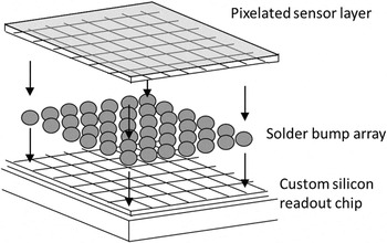
One conceptually simple, but powerful, imaging detector design is the “hybrid pixel” structure, shown in Figure 1 . A pixelated semiconductor sensor is connected face to face with a custom-designed silicon readout chip by a fine array of solder balls. Each pixel in the sensor is connected to a channel of readout electronics on the chip. This design makes it possible to achieve direct detection in a relatively thick sensor layer with small pixels. The readout chip can provide sophisticated signal processing in each individual pixel and fast readout. X-ray diffraction experiments have greatly benefited from “photon counting” readout chip designs such as Pilatus Reference Schmitt, Brönnimann, Eikenberry, Hülsen, Toyokawa, Horisberger, Gozzo, Patterson, Schulze-Briese and Tomizaki3 and Medipix, Reference Ponchut, Rigal, Clement, Papillon, Homs and Petitdemange4 which count the x-ray photons hitting each pixel during the acquisition. This approach achieves effectively “noise-free” x-ray detection (limited by photon statistics), even over long acquisition periods. This, combined with high readout speed, can greatly improve the speed and sensitivity of measurements.
Diagram of the “hybrid” pixel detector structure, where a pixelated sensor layer is connected by an array of solder bumps to a silicon readout chip providing readout electronics for each individual pixel.

The hybrid pixel detector structure is particularly important because it is compatible with a range of different semiconductor materials, rather than just silicon. The rest of this article discusses the state and future developments of a range of so-called “high-Z” (high atomic number) semiconductor detectors. While these materials have been used to build detectors with a small number of pixels for spectroscopic measurements, a major new field of development is the use of these materials to build imaging detectors with millions of pixels using this hybrid pixel design.
“High-Z” semiconductors
Silicon is the most commonly used semiconductor sensor material, due to its various advantages. Silicon wafer processing technology is mature; silicon wafers are available with near-perfect crystal quality; low leakage current can be achieved by using a photodiode structure; and silicon sensors are relatively robust, both mechanically and chemically.
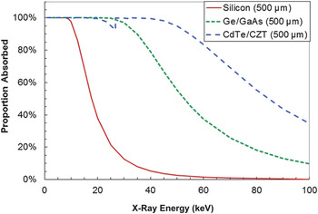
However, the x-ray absorption efficiency of silicon is limited at higher energies. As shown in Figure 2 , silicon sensors with a typical thickness of 500 µm provide 90% photoelectric absorption efficiency at 12 keV, but their efficiency rapidly falls as the photon energy is increased beyond this. Reference Berger, Hubbell, Seltzer, Chang, Coursey, Sukumar, Zucker and Olsen5 For many x-ray experiments in synchrotrons, these lower energies are acceptable. Experiments such as protein crystallography use small samples with low-atomic-number elements, so little x-ray penetrating power is needed, and the 1 Å wavelength of 12 keV photons is sufficient to achieve atomic-level resolution. However, harder x-rays are needed for experiments for studying larger samples, samples with higher atomic number, or when working with sample environments such as reaction vessels. This is particularly common in materials science, for example, geological experiments often take place in high-pressure cells. Silicon sensors are thus not the best option for hard x-ray experiments.
Photoelectric x-ray absorption efficiencies of common semiconductor sensor materials, assuming 500-µm sensor thickness. Reference Ponchut, Rigal, Clement, Papillon, Homs and Petitdemange4 Ge and GaAs have similar absorption efficiencies, so one curve (Ge) is plotted; likewise, one curve is plotted for CdTe and CZT. The notch in the curve at 30 keV occurs because, while x-ray absorption tends to fall with increasing photon energy, sudden increases in absorption occur at the point where the photon energy gets high enough to excite the inner-shell (k-shell) electrons of an atom.

Efficient direct detection of hard x-rays can be achieved using so-called “high-Z” (high atomic number) semiconductors such as germanium (Ge), gallium arsenide (GaAs), cadmium telluride (CdTe), and cadmium zinc telluride (CZT). Each of these high-Z materials has its own strengths and weaknesses. With the notable exception of Ge, a common issue is that these materials cannot be produced with the same level of crystal perfection and uniformity as silicon. This is largely due to these materials being compound semiconductors. The weaker bonding strength in higher-Z materials also means that they can more easily be damaged during processing. Defects in these materials (especially at grain boundaries) can have a range of effects. Reference McCluskey and Haller6 Defects can trap free electrons and holes, resulting in a loss of signal and “afterglow” effects in the semiconductor (where carriers are slowly released from traps, producing signal over a long time period after the original x-ray hit). The charge states of these defects can alter the electric field within the sensor, resulting in insensitive low-field regions or distortions in images. Defects increase the rate at which thermally generated leakage current is produced, making it more difficult to distinguish real x-ray hits. These defects can vary with position within a sensor, or be unstable with time and irradiation. Producing large detector-grade crystals and successfully processing them is a key challenge to using these materials in detectors.
Germanium
Unlike most high-Z semiconductors, Ge is an elemental semiconductor, which is a great advantage for producing high-quality crystals. High-purity germanium (HPGe) single crystals are grown through the Czochralski process, Reference Depuydt, Theuwis and Romandic7 with dimensions currently ranging up to about 100 mm in length and diameter. Net impurity concentrations can be extremely low (109 at/cm3) in both p- and n-type Ge over large volumes; this means that detector thicknesses of several cm can be used. Low-dislocation and even defect-free crystals can be grown for specific applications.
However, because of the relatively low bandgap (0.7 eV), HPGe detectors cannot be operated at room temperature due to the large leakage current from thermally generated charge carriers. Until the late 1990s, using liquid nitrogen (LN2) with a boiling temperature of 77 K was the most common solution to cool down HPGe detectors and keep leakage currents in the range of a few pA. Currently, the major manufacturers of HPGe detectors propose LN2-free options for all types of cryostats, using integrated mechanical cooling devices with proven reliability (long mean time to failure) and limited degradation of performance (vibration of electronic parts can create stray electrical signals, so vibration must be minimized).
The detection principle of an HPGe semiconductor detector consists of developing a p–i–n diode structure in which the intrinsic region is sensitive to ionizing radiation when a reverse-bias voltage is applied. Compared to other semiconductors, HPGe presents the best properties for high-resolution and high-efficiency spectroscopy of hard x-rays and γ-rays. These properties are due to excellent mobility of electron and holes, the relatively high-Z (32) and density (5.32 g/cm3), and the availability of large, pure, and high-quality single crystals. For example, an energy resolution of 0.36 keV can be achieved at 60 keV photon energy. Depending on the required performance (thickness requirements for surface layers, reliability, and sensitivity to other radiations), several types of surface contacts can be used for the junction and blocking contact. Reference Darken and Cox8,Reference Knoll9 Li diffusion and B implantation are the most widespread doping techniques for the N+ and P+ contacts, while surface barrier contacts are still used when low-energy x-rays have to be detected. In order to enhance the count rate capability and provide information on interaction position, researchers developed pixelization and segmentation. Reference Gutknecht10
Although bulkier and more expensive than silicon drift detectors (SDDs), dedicated multichannel HPGe detectors are operated in synchrotrons for x-ray fluorescence, extended x-ray absorption fine structure (EXAFS), and imaging Reference Elleaume, Charvet, Berkvens, Berruyer, Brochard, Dabin, Dominguez, Draperi, Fiedler, Goujon and Le Duc11 for their high sensitivity to high-energy photons and excellent spectroscopic performance. Current developments in both detector technology and readout electronics have led to more compact systems with high-efficiency (10-mm-thick HPGe) demonstrating energy resolutions similar to SDDs, at count rates beyond millions of counts per second per channel, providing an alternative to silicon detectors on a larger energy range.
The capability to closely assemble several HPGe crystals in the same cryostat Reference Duchêne, Beck, Twin, De France, Curien, Han, Beausang, Bentley, Nolan and Simpson12 allowed for improvement of detector granularity as well as the development of high-count-rate spectroscopy, in particular, for synchrotron EXAFS beam lines. Reference Oyanagi, Fonne, Gutknecht, Dressler, Henck, Lampert, Ogawa, Kasai and Mohamed13 A large variety of HPGe sensor configurations are used for x-ray applications, depending on the application requirements. Sensors are generally planar with thickness ranging from 0.5–20 mm, with segmentation patterns applied in one or two dimensions (strip or pixel) on one or both contacts, and with pitches ranging from a few tens of micrometers to a few centimeters.
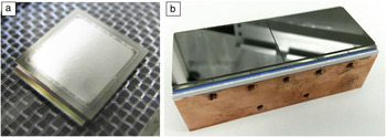
In addition to spectroscopy applications, segmented HPGe detectors have recently been considered for hard x-ray imaging because of their excellent intrinsic charge-collection uniformity. Prototype hybrid pixel detectors have been produced using 1-mm-thick Ge and 55-µm pixel size. Compared to other sensor materials, HPGe wafers offer high crystal perfection, and as a result, these prototypes have shown good image uniformity. Reference Pennicard, Struth, Hirsemann, Sarajlic, Smoljanin, Zuvic, Lampert, Fritzsch, Rothermund and Graafsma14,Reference Sarajlić, Pennicard, Smoljanin, Hirsemann, Struth, Fritzsch, Rothermund, Zuvic, Lampert, Askar and Graafsma15 An image of one of these prototypes, with an array of 256 × 256 pixels, is shown in Figure 3a. However, due to the challenges of cooling these detectors during operation, further development is required to build large-area systems for practical use.
(a) Ge hybrid pixel detector prototype, with a sensor of 256 × 256 pixels (55-µm pixel size) bonded to a single Medipix3 readout chip. (b) Larger GaAs hybrid pixel detector, with two sensor tiles of 768 × 512 pixels (each bonded to six Medipix3 chips) mounted on a single circuit board.

Gallium arsenide
GaAs is widely used in applications such as optoelectronics, and is available in large wafers (6 in.), which makes it an appealing option for radiation detection. However, detecting x-rays requires a combination of good carrier transport, high resistivity, and large sensor thickness (hundreds of micrometers), which is difficult to achieve with GaAs, particularly in bulk crystal growth. In recent years, it has been shown that this combination of qualities can be achieved by taking n-type GaAs (which does not have high resistivity) and compensating for excess electrons with chromium doping.
It is experimentally shown that a material with resistivity of about 109 Ω cm, which is close to the theoretical limit, Reference Tyazhev, Budnitsky, Mokeev, Novikov, Zarubin, Tolbanov, Shelkov, Hamann, Fauler, Fiederle, Procz and Fiederle16 can be produced using this technology. This is high enough to allow using GaAs detectors with a simple photoresistor structure. Optimization of compensation conditions makes it possible to achieve good uniformity of the resistivity distribution, both across the area and thickness of the wafers. This technology can currently be applied to GaAs wafers of up to 1 mm in thickness. Experiments also show that the electric field in high-resolution GaAs sensors is distributed uniformly throughout the thickness of the high-resistive layer. Reference Tyazhev, Budnitsky, Koretskay, Novikov, Okaevich, Potapov, Tolbanov and Vorobiev17 Finally, investigations of the charge collection efficiency have shown reasonable charge-transport properties. With a strong electric field applied to the detector, the mean distance traveled by carriers before they are trapped is on the order of 5–10 mm for electrons and 50–100 µm for holes; this is acceptable, but lower than for other materials discussed.
It was shown that by using detectors with small pixels (to reduce the influence of hole transport on signal collection), it is possible to obtain an energy resolution of about 2–3 keV at 60 keV in the temperature range from 7°C to ambient. Reference Veale, Bell, Duarte, French, Schneider, Seller, Wilson, Lozinskaya, Novikov, Tolbanov and Tyazhev18 Therefore, GaAs is less suited to spectroscopic detectors than other materials. However, GaAs is a promising material for hybrid pixel detectors, due to its relative robustness and stability. GaAs detectors have been constructed with 55-µm pixel size and readout with Medipix Reference Ponchut, Rigal, Clement, Papillon, Homs and Petitdemange4 chips. These detectors show a spatial resolution close to the theoretical limit given by the pixel size. Reference Hamann19 Raw x-ray images taken with these detectors show a cellular structure due to the dislocation network emerging during crystal growth of n-GaAs. However, the good stability of the detector response over time makes it possible to perform “flat-field” correction, which greatly improves the image quality. Reference Hamann, Koenig, Zuber, Cecilia, Tyazhev, Tolbanov, Procz, Fauler, Baumbach and Fiederle20
GaAs hybrid pixel detectors have been produced with 768 × 512 pixels with 55-µm pixel size layout and operated with the “LAMBDA” readout system. Reference Pennicard, Smoljanin, Struth, Hirsemann, Fauler, Fiederle, Tolbanov, Zarubin, Tyazhev, Shelkov and Graafsma21 These systems can be operated at 2000 frames per second with no deadtime between images. Diamond anvil cell experiments have shown that a single 0.5 ms image is sufficient to produce a useful diffraction pattern, thus demonstrating that these detectors can enable high-speed experiments with hard x-rays. Multiple sensors may be tiled together to create multi-megapixel GaAs systems. An image of a GaAs detector module composed of two tiles on a single circuit board is shown in Figure 3b.
As the brilliance of synchrotron sources increases, radiation hardness and stability become increasingly important. Studies of radiation hardness of GaAs sensors with small pixels were conducted using x-rays from the dynamic light scattering synchrotron. Reference Veale, Bell, Duarte, French, Hart, Schneider, Seller, Wilson, Kachkanov, Lozinskaya and Novikov22 It was found that the radiation hardness of the sensor was at least 1 MGy after irradiation with 12 keV x-rays. Studies of high-flux x-ray imaging using GaAs:Cr Timepix assemblies have shown that the count rate of 16 keV photons reaches values of 1 × 10⁹ s–1 mm–2. Reference Hamann, Koenig, Zuber, Cecilia, Tyazhev, Tolbanov, Procz, Fauler, Fiederle and Baumbach23 It should be noted that with 10 h exposure of the sensor, there were no effects connected to polarization or radiation damage.
Cadmium telluride
For experiments with extreme x-ray energies and smaller pixel sizes, CdTe is an appealing option, because the higher atomic numbers of Cd and Te (48 for Cd, 52 for Te) result in significantly shorter x-ray attenuation lengths compared to Ge and GaAs. As shown in Figure 2, 500 µm of CdTe will absorb 55% of 80 keV photons. CdTe is used for applications such as thin-film solar cells, and nearly all the CdTe used for x-ray detection is manufactured by Acrorad, Japan.
Detector-grade CdTe is generally produced by first growing polycrystalline CdTe ingots from a Te-rich melt, and then progressively recrystallizing the material by the traveling heater method (THM). Reference Shiraki, Funaki, Ando, Tachibana, Kominami and Ohno24 Using this approach, 4-in.-dia. single crystal wafers of CdTe can be reliably produced. The carrier transport properties of the material reveal that the mean distance before trapping is on the order of 1 cm for holes and 10 cm for electrons in good quality bulk material; while this is lower than for Ge and Si, it is sufficient for good spectroscopic performance. Reference Takahashi and Watanabe25
Defects in CdTe may cause a range of problems, and due to the fragility of the material, some defects such as dislocations can be introduced during processing, for example, mechanical force can cause atomic planes to slip with respect to each other. One particular issue with CdTe is “polarization,” where the electric field within the sensor changes with time and irradiation due to trapping of electrons and holes by crystal defects. Under high-flux conditions, this trapped charge can build up to the point where the electric field collapses, resulting in a loss of signal. Improvements in crystal growth over time have made it possible to apply CdTe to x-ray applications with higher flux.
The effects of polarization depend on the contact technology used. By using different metals for electrodes, it is possible to create Schottky contacts with the material (giving diode-like behavior) or conductive (ohmic) contacts. Schottky contacts reduce current flow in the sensor, resulting in better spectroscopic performance, but polarization tends to increase. Significant signal loss after operating a Schottky contact detector for 60 min in low irradiation conditions is reported in Reference Reference Funaki, Ando, Jinnai, Tachibana and Ohno26. However, this can be combatted by temporarily switching off the high voltage on the sensor. Ohmic contacts are more commonly used for high-count-rate applications.
As a concrete example of spectroscopy with CdTe, the “hexitec” spectroscopic pixel detector (a hybrid pixel detector with a layout of 80 pixels × 80 pixels of 250-µm size) achieves a spectral response of better than 1.2 keV full width at half maximum at 60 keV in 93% of pixels. Reference Wilson, Dummott, Duarte, Green, Pani, Schneider, Scuffham, Seller and Veale27 While this is a spectroscopic detector, its large number of pixels allows it to be used for novel forms of spectroscopic imaging in synchrotrons. Reference Wilson, Connolley, Dolbnya, Grant, Liotti, Lui, Malandain, Sawhney, Seller and Veale28
Photon-counting hybrid pixel detectors for x-ray diffraction experiments at synchrotrons have also been built with higher pixel counts and smaller pixel sizes. The largest CdTe systems are currently manufactured by Dectris, with up to two megapixels and a pixel size of 172 µm. Detectors based on Medipix readout chips have been produced with 55-µm pixel sizes and are used in high-resolution imaging experiments. Reference Diemoz, Bravin, Sztrókay-Gaul, Ruat, Grandl, Mayr, Auweter, Mittone, Brun, Ponchut and Reiser29
As the pixel size decreases, the effects of localized nonuniformities in the material such as dislocations become more noticeable. For example, x-ray images reported in Reference Reference Ruat and Ponchut30 show a network of lines appearing in the detector with distorted count rates, most likely due to dislocations in the sensor. Long experiments and high x-ray fluxes can also cause polarization effects, reducing the effectiveness of image correction, though the count rate that can be achieved with these detectors is sufficient for most experiments. For example, CdTe detectors using the Timepix chip can cope with x-ray fluxes of up to 105 photons/s/pixel (approximately 40 million counts/mm2/s), limited by the chip, but high-flux irradiation for extended periods of time has been shown to temporarily alter the flat-field response.
Cadmium zinc telluride
Much of the previous discussion of CdTe also applies to CZT detectors. Replacing some Cd atoms with Zn to give Cd1–x Zn x Te increases the bandgap of the material from 1.44 eV to approximately 1.6 eV for typical Zn concentrations of x = 0.08 to 0.15, and the wider bandgap has the benefit of lower leakage current, which can improve spectroscopic behavior. Reference Takahashi and Watanabe25
Different growth methods are used for CZT. The high-pressure Bridgman technique produces large, polycrystalline CZT ingots, which can then be diced to obtain single crystals, typically up to a few cubic centimeters. This can provide CZT for spectroscopic detectors, but imaging detectors typically require larger single-crystal areas. However, recent advances applying THM growth Reference Iniewski, Rissi, Radicci, Zambon, Schneebeli, Iwanczyk, Butler and Bosch31 to CZT has made imaging more feasible.
As previously described for CdTe, high-flux operation of CZT sensors presents well-known challenges primarily due to material defects that lead to polarization and other instability effects. Reference Awadalla32 Experimental results have shown that low electron and hole collection occurs in regions where polarization has been induced. Reference Prekas33
Improvements in THM growth and device fabrication that require additional processing steps have enabled CZT to show dramatically improved hole-transport properties and reduced polarization effects. As a result, high-flux operation of CZT sensors at rates in excess of 200 million counts/s/mm2 is now possible and has enabled multiple medical-imaging original equipment manufacturers to start building cameras for computed tomography, baggage scanning, and nondestructive testing (NDT). While few CZT imaging detectors have been produced for synchrotron applications thus far, these developments in CZT make it a promising option for the future.
In order to prepare for high-volume commercial production, the CZT industry is moving from individual tile processing to whole-wafer processing using silicon methodologies. Parametric-level screening is being developed at the wafer stage to ensure high wafer quality before detector fabrication in order to maximize production yields. These process improvements enable CZT manufacturers to provide high-volume production for photon-counting applications in an economically feasible manner.
CZT sensors are capable of delivering both high count rates and high-resolution spectroscopic performance, although it is challenging to achieve both of these attributes simultaneously. Recent publications discuss material challenges, detector design tradeoffs, and hybrid pixel readout chip architectures required to build cost-effective CZT-based detection systems. Reference Iwanczyk34 Photon-counting readout chips are an essential part of the integrated module platforms, because simpler readout chips that integrate the signal in each pixel over a period of time cannot make accurate energy measurements if more than one photon per image hits the pixel. Reference Iniewski35
CZT sensors are finding widespread use in medical imaging (single photon emission computed tomography, dental imaging), NDT, dirty bomb detection, and baggage scanning. Technological development and innovation in CZT-based imaging is proceeding at a rapid pace. New CZT sensor technologies for spectral multi-energy image acquisition are being developed, driven by the demands of the field of radiology for better quality images of tiny moving structures, as well as a push toward novel material/tissue characterization. Reference Schlomka, Roessl, Dorscheid, Dill, Martens, Istel, Bäumer, Herrmann, Steadman, Zeitler and Livne36
Conclusions
Semiconductor detectors are widely used in synchrotrons, but there is still room for improvements in semiconductor materials for hard x-ray detection. While a mature technology, Ge detectors are now being developed for a wider range of synchrotron experiments such as imaging. GaAs has good potential for building imaging detectors. CdTe and CZT can achieve good spectroscopic performance, and are increasingly feasible for building large-area detectors capable of coping with high x-ray fluxes.
Acknowledgment
The authors would like to thank W. Inui for advice on CdTe detectors.

David Pennicard is Chief Technology Officer of X-Spectrum GmbH, a detector company based in Hamburg, Germany, and a detector scientist at Deutsches Elektronen-Synchrotron, Germany. He received his PhD degree in physics from the University of Glasgow, Scotland, UK, in 2009. His research interests focus on x-ray detectors for synchrotrons and high-Z semiconductor materials. He led the development and commercialization of the “LAMBDA” photon-counting detector. Pennicard can be reached by phone at +49-40-8998-4544 or by email at david.pennicard@x-spectrum.de.

Benoît Pirard manages R&D and Specialty Detector Developments at Mirion Technologies (formally Canberra), France. He received his PhD degree in astrophysics from the University of Toulouse, France, in 2006. Previously, he was an associate researcher at the University of Bern, Switzerland, and at IRAP, France. His research interests focus on the development of high-purity germanium detectors for advanced scientific applications in fundamental research and in industry. Pirard can be reached by phone at +33 (0)3 88 77 49 80 or by email at bpirard@mirion.com.

Oleg Tolbanov is a full professor and head of the Functional Electronics Laboratory in the Semiconductor Electronics Department of Tomsk State University, Russia. His research interests focus on the electronic properties of semiconductor structures doped with deep-level impurities and the development of devices. He is one of the creators of GaAs:Cr structures and matrix sensors. He has authored more than 300 scientific publications and holds approximately 50 patents. Tolbanov can be reached by phone at +79610984838 or by email at top@mail.tsu.ru.

Krzysztof Iniewski manages R&D development activities at Redlen Technologies Inc., a detector company based in British Columbia, Canada. He manages the development of highly integrated cadmium zinc telluride detector products in medical imaging and security applications. He received his PhD degree in electronics from the Warsaw University of Technology, Poland, in 1988. He has held various management and academic positions at PMC-Sierra, University of Alberta, Simon Fraser University, The University of British Columbia, and University of Toronto, Canada. Iniewski can be reached by email at kris.iniewski@gmail.com.