Introduction
Since its invention by Shockley, Bardeen, and Brattain in 1947,Reference Riordan, Hoddeson and Herring1 the transistor has become the fundamental building block of almost all modern electronic circuits and systems. Its importance stems from the fact that an electrical signal applied between one pair of terminals controls the current flowing through another pair of terminals. This allows transistors to function as amplifiers or switches of electrical signals that enable logic operations and power generation/management.
Today, Si transistors can be mass produced cheaply on a per-device basis with a high yield and tight specifications using highly automated and highly scalable semiconductor manufacturing processes. Advances in fabrication technology have resulted in a rough doubling of transistor counts per integrated circuit every two years, in accordance with Moore’s Law.Reference Moore2 While Si has proven to be exceptionally suitable for digital processing and logic applications, it loses out to other materials such as the III–V compound semiconductors for radio frequency (RF), high power, and optoelectronic applications.
Benefits of metamorphic transistors
Transistors can be made from new materials with relative simplicity if a starting substrate with identical crystal structure and lattice parameters are available for the desired device material. However, if no such native substrate exists, metamorphic epitaxy is required. This is especially the case when dealing with the III–N material system, where large-area bulk GaN or AlN substrates are not readily available.
Additionally, metamorphic epitaxy affords circuit designers access to lattice constants and material properties (e.g., bandgap, mobility) that cannot be readily grown on commercially available binary substrates (e.g., GaAs, InP). A key example is the use of metamorphic buffer layers to access In0.3Ga0.7As and In0.3Al0.7As alloys that have lattice constants between those of GaAs and InP for metamorphic InAlAs/InGaAs high-electron-mobility transistors (HEMTs). Their higher carrier mobility compared to AlGaAs/GaAs HEMTs, and larger channel bandgap than conventional InP/In0.53Ga0.47As HEMTs, potentially offer a superior combination of speed and breakdown for various applications.Reference Zaknoune, Ardouin, Cordier, Bollaert, Bonte and Theron3 Another potential avenue for performance improvements is nanopatterned metamorphic epitaxy that uses selectively grown III–V materials to create high-mobility channels on a Si platform.
Even when appropriate bulk substrates are available, metamorphic techniques allow for the use of cheaper and larger non-native substrates that may offer significant production cost reduction, such as the use of GaAs substrates for InP-based HEMTs and heterojunction bipolar transistors (HBTs).Reference Ng, Radhakrishnan and Wang4 GaAs substrates are cheaper, available in larger sizes, and less fragile than InP substrates; consequently, they can reduce per-die device fabrication costs and improve yields, especially for circuits that consume larger die areas like microwave monolithic integrated circuits.
From this perspective, the ultimate starting substrate is Si, as it is inexpensive, is readily available in large sizes (200 mm and larger), can have very high electronic quality, is mechanically robust, and possesses very good uniformity and tolerances. However, with the end of Moore’s Law scaling approaching, achieving metamorphic devices on large-area Si substrates is important for yet another reason—to match Si substrate sizes for wafer-scale integration of non-CMOS (complementary metal oxide semiconductor) and Si CMOS devices to form a truly monolithic integrated circuit.
There are two main types of transistors: field-effect transistors (FETs) and bipolar junction transistors (BJTs). Metamorphic versions of both entail similar benefits as described previously. Nevertheless, because FETs are planar devices (i.e., device terminals arranged in the same plane) and BJTs are non-planar devices, the former are more amenable to very large-scale integration. The rest of this article will therefore focus on FETs, as they offer an easier path toward integration with Si CMOSs.
Metamorphic epitaxy
Lattice mismatch and coefficient of thermal expansion mismatch
For a single-crystal film with lattice constant a f on a single-crystal substrate with lattice constant a s, a lattice mismatch, f lattice, arises that is defined with positive stresses and strains being tensile, while negative values are compressive:
 $${f_{lattice}} = {{{a_s} - {a_f}} \over {{a_f}}}$$.
Furthermore, if the film is grown at temperature T g and is then cooled down to room temperature, T room, an additional coefficient of thermal expansion (CTE) mismatch stress develops:
 $${\sigma _{CTE}} = {Y_f}\left( {{T_g} - {T_{room}}} \right) \cdot \left( {{\alpha _f} - {\alpha _s}} \right)$$.
This mismatch depends on the difference between the film’s (α f) and substrate’s (α s) CTEs and on the film’s elastic modulus, Y f. Materials that are highly dissimilar in terms of lattice constants and CTEs, or grown at high temperatures, will face more severe challenges.
With metal–organic chemical vapor deposition (MOCVD) growth temperatures ≥700°C for III–As/P and ≥1000°C for III–N materials, significant stresses build up between the epitaxially grown films and the substrates when the wafers and device layers are ultimately cooled down to room temperature. Bowing of the wafer in proportion to its size occurs and, if large enough, will impact fabrication yields. Device performance might also be affected, as strain effects modify both the electrical and optical properties of the materials. In extreme cases, the large internal film stresses lead to wafer fragility issues that further impact device and circuit yield.Reference Zhu, McAleese, McLaughlin, Häberlen, Salcianu, Thrush, Kappers, Phillips, Lane, Wallis, Martin, Astles, Thomas, Pakes, Heuken and Humphreys5
Metamorphic graded buffers for lattice engineering
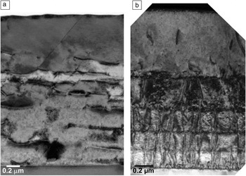
As described in the introductory article in this issue, graded buffer layers are commonly used for metamorphic transistor devices. Because dislocations have a negative impact on devices, the goal is to keep the threading dislocation density (TDD) low enough so as not to affect subsequent device operation while engineering the lattice constant. This is generally achieved by growing one or more buffer layers with intermediate lattice constants to bridge the difference between the starting lattice constant and the desired ending lattice constant. III–V compound semiconductors especially benefit from metamorphic epitaxy, as they can readily form alloys with different lattice constants. In particular, the III–As/P and III–N material systems have been used extensively for transistors due to their favorable electronic properties. Cross-sectional transmission electron microscope (TEM) images of typical graded buffers used in the III–As/P and III–N material systems are shown in Figure 1.
Cross-sectional transmission electron microscope images of an (a) InAlAs continuously graded buffer (taken in two-beam diffraction condition with diffraction vector, g = 〈022〉); and an (b) AlGaN step-graded buffer (taken with g = 〈0002〉).Reference Lee, Bao, Kohen, Huang, Lee, Fitzgerald and Tan47

III–As/P metamorphic epitaxy
In the III–As/P material system, compositionally graded InxAl1–xAs buffers are generally used for metamorphic transistor growth due to their larger bandgap which results in low buffer leakage currents.Reference Hoke and Whelan6 This is especially critical for high-speed radio frequency (RF) devices, the general application focus for As/P transistors, and is why InAlAs is strongly preferred, despite the greater difficulties of working with Al-containing materials. Starting from a GaAs (or AlAs) layer, the InAlAs buffer is typically step-graded or continuously graded, by changing the In mole fraction of the alloy in discrete steps or in a continuous fashion, respectively. InGaP-graded buffers have also been used due to their significantly better thermal conductivity, which is important for high-power devices.Reference Ng, Radhakrishnan and Wang4
Slower composition grading rates moderate the pace of strain incorporation into the growing films (generally resulting in lower TDD), but result in thicker metamorphic buffers that might exacerbate CTE mismatch issues. Strain fields that develop as lattice-mismatch strain is added and subsequently relaxed lead to characteristic “crosshatch” surface roughness.Reference Lee and Fitzgerald7 This surface roughness must be managed such that dislocation motion is not impeded during metamorphic buffer growth, and channel mobility is not significantly affected. Higher growth temperatures are generally preferred to enhance glide velocities and mismatch relaxation in III–As/P materials. However, too high a growth temperature can lead to excess dislocation nucleation and may also cause increased surface and interface roughness.
As mentioned in the article by France et al. in this issue, phase separation is a key challenge in metamorphic growth of III–V materials. This affects graded buffer quality in two ways: (1) Strain fields at the boundaries of different compositional domains can arrest dislocation glide; (2) lattice mismatch at the boundaries can itself promote the nucleation of excess dislocations.Reference Quitoriano and Fitzgerald8 With particular relevance to metamorphic transistors, phase separation has been observed in InGaAs, InAlAs, InGaP, and AlGaN alloys,Reference Quitoriano and Fitzgerald8–Reference Chen, Chua and Miao10 the most common ternary alloys used in metamorphic transistors and their associated buffer layers. Phase separation is governed by surface thermodynamics, but it can also be kinetically suppressedReference Yang, Bulsara, Lee and Fitzgerald11 by growing films at low temperatures. Thus, there are generally two growth temperature regimes used to obtain high-quality metamorphic buffers—a high-temperature window where miscibility gaps and phase separation are reduced while dislocation glide is enhanced, and a low-temperature window where phase separation is ameliorated by kinetically reducing atomic mobility. It should be noted at this point that phase separation is also mediated by the presence of strain.Reference Lee and Fitzgerald12
III–N metamorphic epitaxy
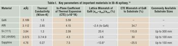
With no readily available large-area GaN or AlN bulk substrates on which III–N devices can be directly grown, metamorphic epitaxy is a necessity. The most commonly used substrates for III–N epitaxy are Si (111), SiC, and sapphire. Their key parameters are shown in Table I,13 along with values for GaN and AlN.
Key parameters of important materials in III–N epitaxy.13

*to (11 $\bar 2$0) planes.
Note: a, lattice parameter; a sub, substrate lattice parameter; a GaN, GaN lattice parameter; 4H/6H, SiC polytypes.
Si (111) wafers are desirable due to the availability of relatively low-cost 200-mm or larger diameter wafers. However, they present the most challenging lattice-mismatch situation at +20.8%. Additionally, the CTE of Si is less than one-half that of GaN, and thus, the GaN films contract far faster than the Si substrate during cooldown from the high nitride growth temperatures. Even if the wafer does not crack under the high tensile stress, it would likely possess a significant bow, especially at larger wafer sizes, making subsequent device processing challenging. Furthermore, there are a host of other issues related to nucleating and growing III–N materials on Si,Reference Semond14 including meltback etching, where uncontrolled Ga and Si alloying at the GaN–Si interfaceReference Dadgar15 rapidly destroys the growing nitride film once the process initiates. Alternatively, AlN nucleation layers and subsequent growth of partially relaxed (Al)GaN layers with compressive strain can compensate for the tensile stress that builds up during cooldown due to CTE mismatch. This provides a measure of wafer bow control and can reduce the propensity of the GaN-on-Si wafer to crack during growth and cooldown through balancing the internal stresses of the different layers.
Nanopatterned metamorphic epitaxy
With increasing implementation of high strain layers and three-dimensional (3D) device structures such as fin field-effect transistors (finFETs), advanced CMOS foundries are also exploring novel methods to implement metamorphic epitaxy such that III–V channels can be directly incorporated into the CMOS processing line. As mismatched epitaxial growth in small growth windows has been shown to result in reduced dislocation densities,Reference Fitzgerald16 many different nanopatterned growth strategies have been introduced over the years, and two are briefly reviewed here.
In one approach, narrow on-axis (001) silicon ridges are defined by closely spaced shallow trench isolation (STI) features. Chemical etching of the ridges results in trenches between the STI features with V-groove Si (111) surfaces at the bottom of the trench on which MOCVD is used to selectively grow a relaxed InP metamorphic buffer. The narrow STI sidewalls provide defect trapping that eliminate threading dislocations, twins, and stacking faults. This buffer is partially removed, and an InGaAs channel that is lattice-matched to the InP buffer is grown. Implementing a gate-all-around FET device structure has yielded devices with a channel length (L G) of 60 nm with peak transconductance of 1030 µS/µm and a subthreshold swing of 125 mV/dec, which are values that compare favorably with other reported results.Reference Waldron, Merckling, Teugels, Ong, Sebaai, Barla, Collaert and Thean17
In another approach, a silicon-on-insulator wafer is first patterned and etched to produce a silicon seed region. MOCVD is then used to laterally grow InAs nanowires in a process termed template-assisted selective epitaxy. With horizontal III–V channels that demonstrate a Hall mobility of 5400 cm2/Vs, multiple-gate FETs exhibit a peak transconductance of 1000 µS/µm at a drain–source voltage (V DS) of 0.5 V.Reference Schmid, Borg, Moselund, Gignac, Breslin, Bruley, Cutaia and Riel18
Metamorphic FETs
FETs are used in all types of applications spanning digital logic, direct current, power, analog/mixed-signal, and RF. As such, device characteristics and figures of merit have to be appropriately tailored, and often, multiple device options and tradeoffs need to be considered.
Metamorphic growth techniques have generally been adapted to HEMTs and metal oxide semiconductor field-effect transistors (MOSFETs), the two most promising types of FETs today. III–V MOSFETs with good device performance have become possible due to the development of high-quality dielectric film deposition using techniques such as atomic layer deposition, which has made it possible to form MOS structures with good oxide–semiconductor interfaces, even in III–V devices.Reference del Alamo, Antoniadis, Guo, Kim, Kim, Lin, Lu, Vardi and Zhao19,Reference Matocha, Chow and Gutmann20 The distinctions between HEMTs and MOSFETs have blurred somewhat, especially for InGaAs-based devices. MOSFET designers have sought to increase electron mobility by leaving channel layers undoped and burying them such that they are not in direct contact with the gate dielectric. Conversely, HEMT designers have moved toward insulated gates to reduce gate leakage currents, leading to metal–insulator–semiconductor HEMT and metal oxide semiconductor HEMT (MOSHEMT) structures.Reference Yagi, Shimizu, Inada, Yamamoto, Piao, Okumura, Yano, Akutsu and Ohashi21–Reference Mo, Wichmann, Roelens, Zaknoune, Desplanque, Wallart and Bollaert24 These structures share many similarities with buried-channel MOSFETs, especially quantum-well FETs that also rely on delta-doped barriers (i.e., barrier layers containing a doped plane of carriers) to supply carriers for the two-dimensional electron gas (2DEG) conducting channel.Reference Radosavljevic, Chu-Kung, Corcoran, Dewey, Hudait, Fastenau, Kavalieros, Liu, Lubyshev, Metz, Millard, Mukherjee, Rachmady, Shah and Chau25
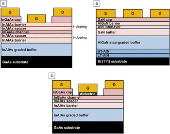
Figure 2 shows schematics of a typical III–As/P HEMT, a III–N metamorphic HEMT (mHEMT), and a III–As/P metamorphic MOSFET. The substrates are depicted in black; the metamorphic buffer layers that are used to modify the effective lattice constant are depicted in blue shades; and the device layers are depicted in red shades.
Schematics of typical metamorphic (a) InGaAs high-electron-mobility transistor (HEMT), (b) GaN HEMT and (c) InGaAs metal oxide semiconductor field-effect transistor. The metamorphic buffer layers are in blue, while the device layers are in red. Note: S, source; D, drain; G, gate; HT, high (growth) temperature; LT, low (growth) temperature; δ-doping, planar doping layer.

Metamorphic InGaAs HEMTs/MOSFETs
In the III–As/P material system, HEMT characteristics are determined mostly by the (In)GaAs channel material. Metamorphic buffers are used to tune the lattice constant to allow access to a specific channel (InGaAs) and barrier (typically InAl(Ga)As) material combination. Higher indium mole fractions in the channel result in higher mobility and faster devices. Additionally, delta doping is usually employed to provide the carriers in the channel and to reduce the amount of parasitic conduction in the low-mobility barrier layer.Reference Kim, Tian and Littlejohn26
HEMTs with high (≥53%) indium mole fraction InGaAs channels are used for ultrahigh-speed applications, as they have achieved f T (unity gain cutoff frequency) and f max (maximum oscillation frequency) values of several hundreds of GHz, which makes them suitable for THz or near-THz applications.Reference Kim, Brar and del Alamo27,Reference Chang, Kuo, Hsu, Chiang and Miyamoto28 Metamorphic epitaxy has been successfully used by many groups to obtain mHEMTs on GaAs substrates with ≥53% indium mole fraction InGaAs channels, analogous to lattice-matched or pseudomorphic HEMTs on InP substrates. Similar performances for f T, transconductance (g m), gain, noise figure (a measure of the excess noise in the device output over and above that attributable to thermal noise), and reliability have been reported for mHEMT and pseudomorphic HEMT (pHEMT) devices;Reference Ng, Radhakrishnan and Wang4,Reference Komiak, Smith, Duh, Xu and Chao29–Reference Wu, Liu, Li, Li, Hu, Xi and Zhao31 this suggests that the metamorphic buffers did not detract from device performance. For instance, deeply scaled GaAs mHEMTs, such as those reported by Leuther et al.Reference Leuther, Koch, Tessmann, Kallfass, Merkle, Massler, Loesch, Schlechtweg, Saito and Ambacher32 and Kim et al.,Reference Kim, Brar and del Alamo27 have attained f T values of over 660 GHz and maximum linear transconductance, g m,max >2500 mS/mm for devices with channel lengths ranging from 20–40 nm. These values are comparable to those reported for InP pHEMT devices with similar channels and gate dimensions.Reference Chang, Kuo, Hsu, Chiang and Miyamoto28,Reference Kim and del Alamo33 Komiak et al. reported that their mHEMTs had lower additive phase noise at low operating currents than lattice-matched HEMTs on InP substrates, making them superior devices for low-noise amplifier circuits.Reference Komiak, Smith, Duh, Xu and Chao29 They surmised that this unexpected result could be due to the differences in surface trapping effects between the two types of devices.
InGaAs mHEMTs with InGaAs channels with approximately 30–40% indium mole fraction have shown a good balance of speed and power handling/breakdown.Reference Zaknoune, Ardouin, Cordier, Bollaert, Bonte and Theron3,Reference Kim, Koh, Choi, Kim, Kwon and Seo34 Kim et al. reported 50-nm In0.35Ga0.65As channel devices that were grown on metamorphic InAlAs buffers graded from AlAs to In0.45Al0.55As and capped with a grade-back layer of In0.4Al0.6As. The devices achieved f T and f max values of 216 and 400 GHz, respectively, with a relatively high OFF-state breakdown voltage of –7.2 V, making them excellent candidates for high-gain low-noise amplifiers.Reference Kim, Koh, Choi, Kim, Kwon and Seo34
Metamorphic insulated gate devices such as MOSHEMTs and MOSFETs have also been explored. Zhou et al.Reference Zhou, Tang, Li, Chen and Lau35 compared In0.6Ga0.4As channel HEMT and MOSHEMT devices on GaAs wafers fabricated using the same starting wafer material. Affirming the benefits of a MOS gate structure, the gate leakage current of the MOSHEMT was five orders of magnitude lower than that of a similar HEMT device. The same group has also reported comparable results for similar metamorphic MOSHEMTs formed on Si wafers.Reference Li, Zhou, Tang and Lau36 Metamorphic MOSHEMTs have also been shown to be less susceptible to impact ionization as compared with HEMTs, resulting in a reduction of the kink effect in device I d–V d (drain–current–drain voltage) curves.Reference Lee, Yeh, Hsu, Liu and Chou37 While surface-channel MOSFETs have poorer high-frequency performance due to lower channel carrier mobility, their superior gate control makes them promising devices for scaling in the context of Moore’s Law and CMOSs. They also possess better ON-state resistance due to the absence of a resistive barrier layer, making them highly suited for logic devices.Reference del Alamo, Antoniadis, Guo, Kim, Kim, Lin, Lu, Vardi and Zhao19 Both wafer-scaleReference Huang, Chang, Chen, Fan, Lin, Lin, Chu, Lee, Khaderbad, Chen, Lin, Chen, Lin, Lin, Chang, Yang, Leung, Yeo, Jang, Hwang and Diaz38 and selective-areaReference Waldron, Merckling, Teugels, Ong, Sebaai, Barla, Collaert and Thean17 metamorphic growth approaches are being explored.
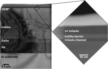
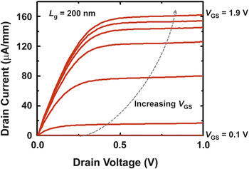
Metamorphic heterostructures have also been grown on lattice-engineered substrates.Reference Yadav, Saeid, Gong, Kohen, Nguyen, Lee, Lee, Yeo, Antoniadis and Fitzgerald39Figure 3 shows a cross-sectional TEM image of a metamorphic In0.3Ga0.7As/InAlAs HEMT heterostructure on Si. Hall measurements revealed a carrier mobility of 5400–5700 cm2/Vs and sheet-carrier densities of approximately 2 × 1012 cm–2. Typical I d–V d results from L g ∼200-nm MOSHEMT devices fabricated on 200-mm-diameter wafer material are shown in Figure 4. The InGaAs cap was co-doped with Te and Si to a level of >1 × 1019 cm–3, and the threshold voltage, V th, was approximately 0.2 V. The device exhibited good pinch-off characteristics, with low drain current (i.e., I d < 10–3 µA/µm) below threshold, and clearly operates as an enhancement mode device. Good ON-state drain currents are achieved, but transconductance collapse is observed at higher gate voltages.
Cross-sectional transmission electron microscope image of an In0.3Ga0.7As/InAlAs high-electron-mobility transistor (HEMT) heterostructure grown on a 200-mm Si wafer. The inset is a high magnification image of the HEMT device layers. The device layers are relatively flat, and no threading dislocations can be seen in the cross section, suggesting a threading dislocation density of <1 × 108 cm–2.

Drain current–drain voltage (I d–V d) curves for a channel length L g = 200-nm metal oxide semiconductor high-electron-mobility transistor device fabricated from heterostructures grown on 200-mm Si wafers. The various curves represent different gate-to-source (V GS) voltages, starting from V GS = 0.1 V for the lowest curve and increasing in steps of 0.3 V to V GS = 1.9 V for the top curve. ON-state current compares favorably with similar devices reported in the literature, though transconductance appears to decrease with increasing gate overdrive (i.e., V GS–V th). Further device design optimization will be needed to address this. Note: V GS, gate-to-source voltage; V th, threshold voltage.

Metamorphic GaN HEMTs/MOSFETs
III–N HEMTs have, to date, been almost exclusively metamorphic devices due to the lack of native bulk substrates. They are exemplified by Al(Ga)N/GaN devices, as depicted in Figure 2b. The dissimilarity of the two polarization components at the AlGaN barrier/GaN buffer-layer heterojunction interface leads to the formation of a deep triangular potential well containing a high-density 2DEG that serves as the conducting channel for the HEMT. Higher aluminum mole fraction barriers result in greater polarization dissimilarity between the barrier and the channel, leading to higher 2DEG sheet-carrier density. This has led to the use of channels with AlN/GaN heterojunctions, in the form of a 1–2-nm-thick AlN interlayer between the GaN channel and the capping AlGaN barrier layer.
The best devices have typically been achieved on SiC substrates due to the lower lattice mismatch and CTE mismatch they present for III–N growth. AlGaN/GaN HEMT heterostructures on SiC substrates have been reported to possess Hall mobilities approaching 2000 cm2/Vs and 2DEG carrier densities approaching 1013 cm–2. This allows L g = 0.25-µm devices to provide output power levels of 7 W/mm at 40 V for 18 GHz devices.Reference Pengelly, Wood, Milligan, Sheppard and Pribble40 Even with their relatively modest Hall mobilities, AlGaN/GaN HEMTs have demonstrated very high f T and f max values on the order of several hundred GHzReference Chung, Hoke, Chumbes and Palacios41 due to their high transconductance. Even higher frequency performance has been obtained in InAlN barrier devices because of their higher 2DEG density.Reference Yue, Hu, Guo, Sensale-Rodriguez, Li, Wang, Faria, Fang, Song, Gao, Guo, Kosel, Snider, Fay, Jena and Xing42
III–N MOSFETs have also been demonstrated in which the conducting channel is formed in a GaN layer without an adjacent Al(Ga)N barrier. There is therefore no 2DEG and no commensurately high carrier mobility.Reference Lee, Cho, An, Bae, Lee, Lee and Hahm43,Reference Im, Ha, Kim, Lee, Kim, Hahm and Lee44 These devices are, however, true enhancement-mode devices with excellent ON-state current to OFF-state current (I ON/I OFF) ratios and low-gate leakage, making them well suited for logic and power applications.
III–V + Si CMOS integration through metamorphic epitaxy
Presently, electronic devices and systems that require integrated circuits that are made of different materials to perform different functions (e.g., Si CMOS for logic and digital processing and III–V for RF front-ends in smartphones) either rely on multiple discrete dies or 2.5D/3D stacking. The former is conceptually simpler and involves using individually packaged microchips of different semiconductor materials and connecting them together on a circuit board. However, this results in interconnect distances between the various functional circuits that are on the order of millimeters or centimeters. The latter involves taking multiple (unpackaged) microchips, placing them in close proximity, and connecting their respective input and output pins with solder bumps and silicon interposers (i.e., electrical routing interfaces between solder bumps). Interconnect distances are reduced by an order of magnitude or more, but this generally requires relatively expensive and serial packaging processes. In both cases, pin counts are limited, constraining the amount of communication possible between the various circuit elements. Additionally, the relatively long interconnect distances between different functional circuit elements result in series resistance power losses and heat dissipation, timing delays, and impedance matching issues for high-speed RF signals.
The holy grail of integrated circuit technology is true monolithic integration of different circuit elements composed of different materials, at an interconnect density and scale on the order of those found in current Si CMOS integrated circuits. Given their superior conduction characteristics and better power-handling capability, III–V transistors (especially in the case of III–N devices) are ideal to use in input and output stages of high-speed wireless or power-management circuits, where Si CMOS devices face limitations. Si CMOS devices can continue to be used in digital logic, processing, and control circuitry, where their capability and density are established. The greatly reduced interconnect distances mean reduced series resistance losses and lower latency between the various circuit functional blocks. Self-sensing and self-tuning features such as envelope tracking can be implemented more efficiently. Circuit designers will have vastly larger design flexibility for better circuit optimization and creation of new functionality through holistic designs that enable simulation of more complex circuits consisting of III–V and Si transistors without pin-count limitations.
However, achieving this in a commercially viable fashion would additionally require being able to process and form interconnects between the different devices using previously established Si CMOS wafer fabrication infrastructure that has already been built with significant investment. This fundamentally requires the ability to grow the III–V material on large-area Si substrates of at least 200 mm, whether via templated regrowth,Reference Im, Ha, Kim, Lee, Kim, Hahm and Lee44 through aspect-ratio trapping techniques,Reference Waldron, Merckling, Teugels, Ong, Sebaai, Barla, Collaert and Thean17 or on a whole-wafer basis. In all cases, some form of metamorphic epitaxy must be performed.
In our earlier work,Reference Liu, Lubyshev, Fastenau, Wu, Bulsara, Fitzgerald, Urteaga, Ha, Bergman, Brar, Hoke, LaRoche, Herrick, Kazior, Clark, Smith, Thompson, Drazek and Daval45 whole-wafer bonding was used to form a silicon on a lattice-engineered substrate that inserted a Ge template layer underneath a Si single-crystal layer. The Si CMOS devices were then formed in the single-crystal Si layer. Next, windows were etched down to the Ge template in which the III–V device layers were regrown metamorphically, followed by III–V device fabrication and interconnection with the earlier-formed Si CMOS devices. While this demonstration proved that monolithic integration was achievable, one limitation was the need to modify the Si CMOS front-end processes to avoid damaging the inserted Ge layer. Another limitation was that the subsequent metamorphic III–V epitaxy had to be performed within a limited thermal budget to avoid damaging the already fabricated CMOS devices.
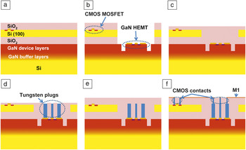
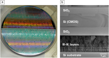
We have developed a III–V + Si integration process that addresses these limitations, allowing the integration of III–V transistors and optoelectronic devices.Reference Fitzgerald, Lee, Yoon, Chua, Tan, Palacios, Zhou, Chang, Kohen, Zhang, Lee, Liu, Chiah and Ge46 We take process design kits (PDKs) from partner Si CMOS foundries and augment them to include III–V circuit elements and integration design rules. The PDKs are used by circuit designers to design monolithic III–V + Si CMOS integrated circuits from the start, as opposed to designing the III–V and Si CMOS circuits separately and having to subsequently deal with their interfacing. Si CMOS device fabrication can be carried out using completely unmodified foundry front-end-of-the-line processes, after which processing is interrupted temporarily. The wafers are then sent to the Singapore-MIT Alliance for Research and Technology Low Energy Electronics Systems Center’s cleanroom facility, where they are combined, using various wafer bonding steps, with 200-mm Si wafers on which complete III–V device heterostructures have been grown via metamorphic epitaxy techniques. The result is III–V + CMOS wafers, each containing a CMOS device layer that is displaced over a III–V device layer with a separation ≤1 µm (Figure 5a).Reference Fitzgerald, Lee, Yoon, Chua, Tan, Palacios, Zhou, Chang, Kohen, Zhang, Lee, Liu, Chiah and Ge46 III–V-device processing, adapted from conventional III–V microfabrication processes to avoid affecting the existing CMOS devices and to be compatible with foundry reentry, is carried out in III–V circuit regions (Figure 5b–d), after which the wafers are reconstituted to resemble the state they originally left the foundry (Figure 5e). The wafers are then returned to the foundry for back-end-of-the-line processing that forms the interconnections between the CMOS and III–V devices (Figure 5f). Such a process flow minimizes the disruption to commercial foundry operations, thereby enhancing the manufacturing viability of our integration process. Figure 6 shows images of a hybrid GaN + CMOS wafer created in our facility. A foundry-processed wafer, in which shallow-trench-isolation features were formed, was combined with a 200-mm GaN-on-Si wafer grown via MOCVD.Reference Lee, Bao, Kohen, Huang, Lee, Fitzgerald and Tan47
Hybrid wafer III–V process flow:Reference Fitzgerald, Lee, Yoon, Chua, Tan, Palacios, Zhou, Chang, Kohen, Zhang, Lee, Liu, Chiah and Ge46 (a) Starting hybrid GaN + CMOS (complementary metal oxide semiconductor) wafer. (b) Window opening and device fabrication in III–V regions. (c) Refilling of III–V windows and planarization. (d) Formation of tungsten (W) plugs that bring the GaN device contacts to the contact plane of the CMOS devices. (e) Redeposition of interlayer dielectric and planarization. (f) Back-end-of-the-line processing (in foundry) to form CMOS contacts and first metal layer (M1) interconnects. Note: MOSFET, metal oxide semiconductor field-effect transistor; HEMT, high-electron-mobility transistor.

(a) Color photograph and (b) cross-sectional transmission electron microscope image of a hybrid GaN + CMOS (complementary metal oxide semiconductor) wafer formed through the Low Energy Electronics Systems wafer integration process.Reference Lee, Bao, Kohen, Huang, Lee, Fitzgerald and Tan47

Metamorphic epitaxy challenges are magnified when attempting growth on large-area substrates. Key among these is large wafer bow due to CTE- and mismatch-related stresses in the films that must be carefully managed to ensure successful wafer bonding, lithography, and that cleanroom processing can be carried out. The challenges are more complex for integration, where the need to reintroduce the III–V + CMOS wafers to the foundry requires the use of SEMI-spec 200-mm Si wafers with 725-µm thickness. For GaN HEMT wafers, we have developed strain-relieving buffer-layer structures and other techniques that allow us to achieve tailorable bow values ranging from –20 to +20 µm over an entire 200-mm wafer. For InGaAs HEMT wafers, bows of <50 µm across a 200-mm wafer are achievable with proper graded buffer-growth parameters.
Conclusion
Though metamorphic epitaxy involves challenges related to the growth of crystalline materials on dissimilar substrates, much progress has been made. Many metamorphic transistor technologies are now effectively mainstream and boast comparable performance values to their lattice-matched counterparts. This large range of device availability allows circuit designers greater opportunity to select the most suitable devices for their desired circuit applications. The next great advance is anticipated to see the use of metamorphic techniques to enable the true monolithic integration of III–V materials and devices with traditional Si CMOS circuits that will allow circuit designers to take advantage of the different benefits offered by the two hitherto distinct integrated circuit worlds.
Acknowledgments
The authors would like to acknowledge the support of the National Research Foundation Singapore through the Singapore-MIT Alliance for Research and Technology’s LEES IRG research program, as well as the members of the LEES team who have contributed to some of the results reported in this article.