I. INTRODUCTION
Buffer leakage in aluminum gallium nitride/gallium nitride (AlGaN/GaN) high electron mobility transistor structures (HEMTs) is recognized to be a serious problem and have deleterious consequences on devices for high-speed, high-power applications.Reference Storm, Katzer, Binari, Shanabrook, Zhou and Smith1–Reference Saito, Noda, Kuraguchi, Takada, Tsuda, Saito, Omura and Yamaguchi5 These devices must support high voltages with small current flow for minimizing power dissipation in the blocking mode of operation. On the basis of these investigations, since the critical electric field for breakdown in GaN-based materials is high, we can attribute some aspects of reduced breakdown voltage and enhanced leakage to the short-circuiting caused by threading dislocations in the nominally undoped GaN buffer layers. Since these investigations clearly demonstrated that dislocations play an important role in leakage and breakdown in these structures, it is important to characterize further the nature of conduction associated with dislocations.
More than 50 years ago, ShockleyReference Shockley6 suggested that dislocations could be “one-dimensional degenerate electron-gas conductors.” He based this postulate on the potential existence of a band of one-dimensional edge states along the core of the dislocation that are partially filled. In a subsequent article, ShockleyReference Shockley7 proposed a row of impurities along the extra half plane of atoms associated with a dislocation that could be conductive. The latter was shown to be consistent with current-voltage measurements, which revealed the presence of a channel conductance path between the emitter and collector of Si junction transistors.Reference Wang8 They concluded that the behavior was consistent with a n-type channel associated with enhanced pipe diffusion of donors down the dislocation core. More recently, density functional theory (DFT) calculations on the core of c-screw dislocations in aluminum nitride (AlN) have revealed the existence of multiple levels in the band gap that can act as conduction pathways for charge carriers.Reference Kioseoglou, Kalesaki, Belabbas, Chen, Nouet, Kirmse, Neumann, Komninou and Karakostas9 This work was stimulated by Ikuhara’sReference Ikuhara10 suggestion that decoration of dislocation cores with impurities could lead to one-dimensional nanostructures for the fabrication of novel materials. On the basis of their DFT calculations, Kioseoglou et al.Reference Kioseoglou, Kalesaki, Belabbas, Chen, Nouet, Kirmse, Neumann, Komninou and Karakostas9 thus proposed that enhanced conduction along the core of doped screw dislocations could act as conducting nanowires in semiconductor films.
In this study, we demonstrate that buffer leakage in AlGaN/GaN heterostructures homoepitaxially grown on bulk GaN substrates is consistent with the concept of dislocations as quantum wires, which is essentially what Shockley originally proposed in the 1950s. To the best of our knowledge, no one has previously reported data that support this hypothesis. Since dislocations are ubiquitous defects in nitride-based materials and can have significant influence on the physical properties, it is important to understand their impact. This is particularly relevant at current stage of device development as buffer leakage in electronic devices has been associated with defects near the epitaxial thin film/substrate interface and can limit the breakdown voltage in device applications.
II. EXPERIMENTAL
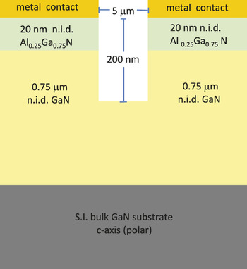
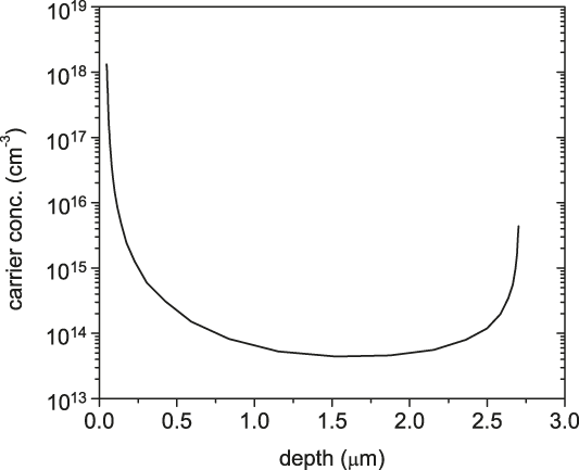
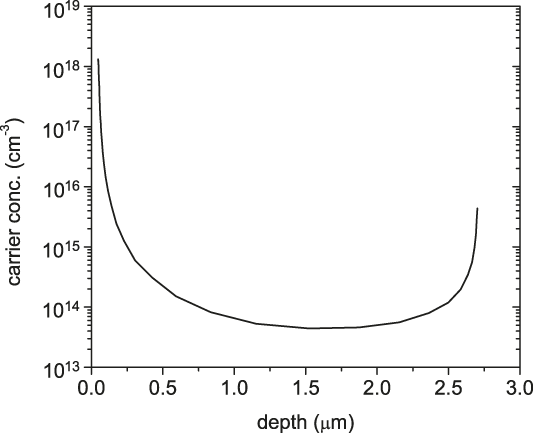
A schematic of the AlGaN/GaN heterostructures grown on 450-µm thick iron (Fe)-doped semiinsulating bulk c-plane GaN substrates is shown in Fig. 1. These heterostructures were grown by metalorganic vapor phase epitaxy at 1040 °C and 60 Torr utilizing trimethylgallium, trimethylaluminum, and ammonia as the precursors. Note that the AlGaN barrier layer was grown without Si doping as the polarization field in GaN-based structures is sufficient to induce a two-dimensional electron gas (2DEG) near the AlGaN/GaN interface. Of particular interest in earlier investigationsReference Grenko, Ebert, Reynolds, Johnson, Hanser, Preble, Paskova and Evans11,Reference Grenko, Ebert, Reynolds, Duscher, Barlage, Johnson, Preble, Paskova and Evans12 was modulation of the mobility with thickness of the GaN buffer. As the buffer thickness decreased from 2 to 0.5 µm, there was a 50% reduction in mobility from ∼1556 to 772 cm2/Vs. Capacitance-voltage measurements of the free carrier concentration versus depth (see Fig. 2) revealed the presence of a charge layer at the heterointerface due to the 2DEG that was associated with the polarization charge and a charge peak at the epitaxial/substrate interface. The latter was shown to contribute ∼1013/cm2 electrons to the sheet concentration of the 2DEG for thin buffers. Subsequent secondary ion mass spectrometry measurements confirmed the presence of peak [Si] concentrations >1019/cm3 at the bulk GaN/epitaxial interface. Areal [Si]areal concentrations were determined to be ∼1.6 × 10¹⁴/cm2, which implied that ∼6% of the interfacial charge contributed to the 2DEG concentration.
Schematic of AlGaN/GaN heterostucture grown on a semiinsulating GaN substrate. Note mesa isolation between contact pads. (color online)

Carrier concentration versus depth from a capacitance-voltage measurementReference Shockley6 of a typical AlGaN/GaN heterostructure grown homoepitaxially on a Fe-doped bulk GaN substrate.
Panchromatic cathodoluminescence (CL) and high-resolution x-ray diffraction measurements were performed for determination of dislocation densities. The panchromatic CL images were obtained in a scanning electron microscope (SEM. Model no. JEOL JSM 6400) at 5 kV that was equipped with an Oxford Instruments MonoCL unit. An x-ray diffractometer (XRD. Philips make; Model no. X’Pert PRO MRD high resolution) with Cu Kα1 radiation and rocking curve and triple axis optics was used for the full width half maximum (FWHM) of the (002) and (105) reflections from which the threading screw and edge dislocation densities can be estimated as outlined below.
After epitaxial growth, the AlGaN/GaN heterostructure wafers were patterned with ohmic contact metal pads 87-µm wide and separated by 5 µm to understand buffer leakage and breakdown; the ohmic metals were rapid thermally annealed at 850 °C for 30 s. As shown in Fig. 1, the ohmic pads were also mesa isolated (∼200 nm). The principle of the technique is to force voltage (50 V) between two adjacent ohmic contact pads and to measure the isolation current then force a known current (100 nA) between pads and measure voltage. We are essentially using this measurement to investigate the influence of the charge at the epitaxial film/substrate interface (see Fig. 2) on buffer leakage and to determine whether the buffer is in breakdown.
III. RESULTS AND DISCUSSION
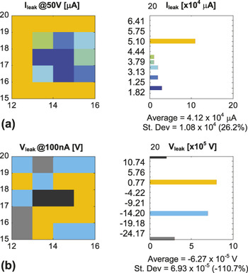
Figure 3 shows typical results of the buffer leakage measurements at constant voltage (a) and constant current (b). An areal map of the distribution of the measured leakage current (a) and voltage (b) over the wafer is shown in addition to the resultant histogram of the data. Multiple measurements gave 43.2 ± 9.3 mA of leakage current at 50 V and −60.1 ± 69.2 µV at 100 nA for constant voltage and current, respectively. The calculated fields are estimated to be an order of magnitude less than the breakdown field, ∼106 V/cm, for GaN, and conduction through the GaN buffer is at least an order of magnitude greater than expected. Hence, an alternative explanation is required since buffer leakage and premature breakdown in GaN-based devices can have significant negative consequences for high-power applications.
Buffer leakage measurements on AlGaN/GaN heterostructures at (a) constant voltage (50 V) and (b) constant current (100 nA), respectively. (color online)

Combining Heisenberg’s energy-time uncertainty relation with Ohm’s law has been shown to enable one to achieve an understanding of the quantum conductance along an electronic channel that is consistent with the Landauer formalism.Reference Zhirnov13 Extending this to N parallel electronic channels and assuming a transmission probability of unity, which implies that transport along the channel is ballistic, the Landauer formula for quantum conductance of these N electronic channels is given byReference Hanson14
 $$G = {\rm{(2}}e^{\rm{2}} {\rm{/}}h{\rm{)}}N\quad{\rm{,}}$$
where e is the electron charge and h is Planck’s constant. Since the quantum resistance is defined as R q = h/2e 2 = 12.9 kΩ, we can then estimate the total resistance of the N electronic channels as
 $$R = R_{\rm{q}} {\rm{/}}N = {\rm{12}}{\rm{.9 \,\,k}}\Omega {\rm{/}}N{\rm{\quad.}}$$
From our AlGaN/GaN HEMT buffer leakage data mentioned above and shown in Fig. 3, using Eq. (2) we can determine that
 $$R = {\rm{1}}{\rm{.16 \,\,k}}\Omega \to N = {\rm{12}}{\rm{.9/1}}{\rm{.16}}\,\sim\,{{11}}$$
or
 $$R = {\rm{0}}{\rm{.6 \,\,k}}\Omega \to N\,\sim\,{\rm{22\quad,}}$$
for constant voltage across the pads or constant current, respectively. That is, using the buffer leakage data presented in Fig. 3 and the expression for the quantum resistance of N electronic channels, we estimate that there are 11–22 electronic channels operative across the metal pads shown in the schematic in Fig. 1.
Panchromatic cathodoluminescence of representative bulk GaN substrates on which these AlGaN/GaN heterostructures have been grown reveal the dislocation density to be ρD ∼ 5 × 10⁶/cm2, which enables one to estimate the spacing between dislocations l D = ρD−½ ∼4.5 µm. Furthermore, high resolution x-ray diffraction analysis of the full width half maximum (FWHM) of the heterostructures is consistent with the CL estimate of the dislocation density as follows. The experimentally determined FWHM of the (002) and (105) reflections were 29 and 31.75 arcsec, respectively. The measured FWHM for the symmetric and asymmetric reflections are given by Eq. (5),Reference Lee, West, Allerman, Waldrip, Follstaedt, Provencio, Koleske and Abernathy15,Reference Grenko, Reynolds, Barlage, Johnson, Lappi, Ebert, Preble, Paskova and Evans16
 $${\rm{\beta }}_{hkl} ^n = {\rm{(\beta }}_{{\rm{tilt}}} {\rm{cos\chi )}}^n + {\rm{(\beta }}_{{\rm{twist}}} {\rm{sin\chi )}}^n + {\rm{(2\pi /}}L{\rm{)}}^n {\rm{/|}}K_{hkl} {\rm{|}}^n {\rm{\quad,}}$$
where βhkl is the measured FWHM of the hkl reflection, βtilt(twist) is associated with the tilt (twist) spread of the rotational distribution, K hkl is the reciprocal lattice vector, n relates to the Lorentzian nature of the fit for the rocking curves of the (002) and (105) reflections (1 < n < 2), and L the coherence length. The screw dislocation density is associated with the FWHM of the tilt component, i.e., the (002) reflection, and given by ρscrew = βtilt2/4.36b screw2 ∼ 2 × 10⁶/cm2 while the edge dislocation density relates to both the (002) and (105) reflections, which gives ρedge = βtwist2/4.36b edge2 ∼ 2 × 10⁷/cm2. The coherence length has been assumed to be L = ∞ in these estimates, which has previously been shown not to be significant.Reference Lee, West, Allerman, Waldrip, Follstaedt, Provencio, Koleske and Abernathy15,Reference Grenko, Reynolds, Barlage, Johnson, Lappi, Ebert, Preble, Paskova and Evans16 On the basis of these dislocation densities determined from x-ray analysis then, the spacing between dislocations is l D = ρD−½ ∼7 µm, which is in reasonable agreement with that determined above by panchromatic CL. Since the metal pad width is 87 µm, one can then estimate from the experimentally determined dislocation density that there are N D = 87/5 = ∼17 dislocations along the width of the ohmic pad, which is consistent with the number of electronic channels calculated from Landauer’s formula above for the quantum resistance using the buffer leakage data. Thus, we suggest that buffer leakage in this AlGaN/GaN heterostructure grown on semiinsulating bulk GaN substrates is associated with dislocations acting as quantum wires in series with electron charge along the epitaxial film/substrate interface due to unintentional Si impurity incorporation. This mechanism is consistent with Shockley’s suggestionReference Shockley6,Reference Shockley7 that one-dimenstional edge states along the dislocation core become degenerate-electron-gas conductors. It is also consistent with DFT calculations on the core of screw dislocations mentioned above that show multiple levels in the band gap that lead to enhanced conduction along the dislocation core and act as a conducting nanowire in nitrides.Reference Kioseoglou, Kalesaki, Belabbas, Chen, Nouet, Kirmse, Neumann, Komninou and Karakostas9 One might question why heteroepitaxial GaN grown on sapphire, SiC or Si substrates does not exhibit orders of magnitude higher leakage as the dislocation densities are >100x of those reported in this study. The distinguishing feature in this study is the presence of the unintentional charge layer along the epitaxial/substrate interface, which acts in series with the dislocations and enables transport between the dislocation conducting channels on either side of the contact pads. This would be analogous to the short circuit between emitter and collector previously observed by WangReference Wang8 in Si junction transistors.
Further considerations are also consistent with the proposed mechanism of buffer leakage in these AlGaN/GaN heterostructures. A conducting channel exists when its diameter is an integral multiple of the half-Fermi wave length.Reference Hanson14 If one assumes that not-intentionally doped (NID) GaN has a Fermi-energy near mid-gap, ∼1.7 eV (this actually underestimates E F as NID GaN is typically n-type), then we estimate the half-Fermi wave length to be
 $${\rm{\lambda }}_{\rm{F}} {\rm{/2}} = h{\rm{/2(2}}m_{\rm{e}} \times E_{\rm{F}} {\rm{)}}^{\rm{\raise.5ex\hbox{$\scriptstyle 1$}\kern-.1em/ \kern-.15em\lower.25ex\hbox{$\scriptstyle 2$} }} {{\sim 1 \,\rm nm\quad,}}$$
which is on the order of the size of the threading dislocation core in GaN, ∼0.6–0.8 nm.Reference Xin, Pennycook, Browning, Nellist, Sivananthan, Omnes, Beaumont, Faurie and Gibart17,Reference Jones, Elsner, Haugh, Gutierrez, Frauenheim, Heggie, Oberg and Briddon18
The concept of one-dimensional extended defects acting as metallic wires was previously reportedReference Lahiri, Lin, Bozkurt, Oleynik and Batzill19 for graphene grown on Ni(111). Scanning tunneling microscopy images revealed the existence of a dislocation line, which was comprised of octagonal and two pentagonal carbon rings. Localized electronic states associated with these rings exhibited a metallic nature. The wave functions of these states are localized at the defect and decay exponentially from the core with a decay length of 0.8 nm, which is on the order of the half-Fermi wave length that we calculated above.
Our analysis of buffer leakage in our homoepitaxially grown AlGaN/GaN heterostructures and the importance of dislocations and interfacial impurities reported above is consistent with conclusions that have been deduced by others. Although the AlGaN/GaN heterostructures in the studies reported in Refs. Reference Storm, Katzer, Binari, Shanabrook, Zhou and Smith1–Reference Zhou, Smith, Storm, Katzer, Binari and Shanabrook3 and Reference Saito, Noda, Kuraguchi, Takada, Tsuda, Saito, Omura and Yamaguchi5 were grown on non-native substrates with an AlN nucleation layer, they have clearly demonstrated that leakage currents are associated with defects near the substrate/epitaxy interface that could be reduced by a lower Al/N ratio during nucleation layer growth. It was suggested that Al-rich nucleation layers lead to increased amounts of Si incorporation near the interface, which increased buffer leakage by several orders of magnitude. Cao et al.Reference Cao, Zimmermann, Xing and Jena4 have shown that buffer leakage can be reduced significantly by incorporating a thin AlN layer at the regrown interface on GaN templates. This polarization-engineered buffer pulls the conduction band up to increase the barrier between the 2DEG and interfacial charge, and thus, reduce high buffer leakage currents.Reference Cao, Zimmermann, Xing and Jena4 The magnitude of reverse-bias leakage in GaN and SiC Schottky diodes has also been shown to occur predominantly at threading dislocations and in particular with screw- and/or mixed dislocations.Reference Hsu, Manfra, Lang, Richter, Chu, Sargent, Kleiman and Pfeiffer20,Reference Fujiwara, Naruoka, Konishi, Hamada, Katsuno, Ishikawa, Watanabe and Endo21 However, scanning Kelvin probe and conductive atomic force microscopy investigations have suggested that the source of leakage in GaN is associated with pure screw dislocations that are uncharged.Reference Simpkins, Yu, Waltereit and Speck22 Nevertheless, the main point that we wish to make is that prior studies have conclusively demonstrated the importance of dislocations and interfacial charge in buffer leakage. The extension of our work is the concept of considering the dislocations in our heterostructures as quantum wires. The concept of threading dislocations acting as highly conducting quantum wires in series with interfacial charge would render these AlGaN/GaN HEMT structures unsuitable for device application due to excessive buffer leakage unless the influence of the interfacial charge can be negated. However, one might envision potential for novel nanostructures in which ballistic transport is desired.
In conclusion, we propose that the buffer leakage which we have measured in our homoepitaxially grown AlGaN/GaN heterostructures is associated with a mechanism based on the concept of dislocations acting as quantum wires in series with unintentional Si impurity incorporation at the bulk GaN substrate/GaN buffer interface. The number of electronic channels deduced from the leakage data using Landauer’s formula for the quantum resistance of N electronic channels is of the same magnitude as the number of dislocations along the ohmic contact pads determined from measurements of dislocation density. This mechanism is consistent with Shockley’s suggestion that dislocations can act as one-dimensional conductors. As we have indicated above, in general the presence of buffer leakage in AlGaN/GaN heterostrucures is considered to be detrimental to electronic and photonic device applications. Nevertheless, one can envision that the concept of dislocations acting as one-dimensional conductors may have potential applications for defect engineering in which ballistic transport is desired.
ACKNOWLEDGMENT
The authors wish to acknowledge Drs. Ralph Cavin and Victor Zhirnov of the Semiconductor Research Corporation, whose lectures on nanoelectronics motivated the authors to think about our buffer leakage problem in this manner.