Introduction
Computers have not only profoundly transformed our lives, they also provide solutions to some of society’s most pressing challenges, from analyzing big data to understanding human language. To meet these and future requirements, faster computing ability and larger data storage are needed.Reference Burr, Breitswisch, Franceschini, Garetto, Gopalakrishnan, Jackson, Kurdi, Lam, Lastras, Padilla, Rajendran, Raoux and Shenory1,Reference Zhu2 However, the huge performance gap between volatile static random-access memory/dynamic random-access memory (SRAM/DRAM) and nonvolatile Flash memory in the storage architecture of current computers (Figure 1a) has become a critical bottleneck for further development.Reference Zhang, Mazzarello, Wuttig and Ma3,Reference Burr, Kurdi, Scott, Lam, Gopalakrishnan and Shenoy4 Since 2008, storage class memory, a term describing emerging memory technologies that may eventually replace Flash and perhaps even DRAM, has been proposed by IBM to bridge this gap.Reference Burr, Kurdi, Scott, Lam, Gopalakrishnan and Shenoy4–Reference Salinga, Kersting, Ronneberger, Jonnalagadda, Vu, Gallo, Giannopoulos, Miredin, Mazzarello and Sebastian7
(a) Performance gap in the storage architecture of a current computer. (b) Photo of 3D Xpoint memory released by Intel in 2015. (c) 1S1R stackable crossbar structure of 3D Xpoint memory, showing a selected memory cell in the high-resistance state (1). (d) Ovonic threshold switch (OTS) + phase-change memory (PCM) in a 3D stackable crosspoint array reported by Intel in 2009. The inset highlights one integrated memory cell consisting of one OTS and one PCM cell. (e) Voltage–current curve of a PCM device, showing ovonic memory switching behavior. (f) Voltage–current curve of an OTS device, distinct from that of PCM. Note: S, selector; M, phase-change memory; CPU, central processing unit; SRAM, static random–access memory; DRAM, dynamic random–access memory.

Phase-change memory, based on the physical structural change between a high-resistance amorphous phase and a low-resistance crystalline phase of chalcogenides, is the most promising candidate in storage class memory.Reference Wuttig and Yamada8–Reference Rao, Ding, Zhou, Zheng, Xia, Lv, Song, Feng, Ronneberger, Mazzarello, Zhang and Ma10 Indeed, the 3D Xpoint, a commercial phase-change memory released by Intel in 2015 (Figure 1b), has demonstrated device performance between DRAM and Flash memory, including operation speed, device lifetime, and storage density.11,Reference Choe12
To achieve the highest 4F 2 (F = feature size) density as Flash memory, the crossbar array seems to be the most attractive device architecture, which has also been used in the 3D Xpoint (Figure 1c).11,Reference Choe12 This device architecture is commonly operated using a “Half-V” select scheme, in which the read voltage is applied to the targeted phase-change memory cell, while other lines in the array remain biased at half the voltage. However, the neighboring cells in the same row or column as the selected cell (half-selected cells) become half-biased and can enable unwanted current pathways known as “sneak currents.”Reference Burr, Shenoy, Virwani, Narayanan, Padilla, Kurdi and Hwang13 This decreases the read sense margin (the difference in total resistance between the 1 and 0 states), increases power consumption, and limits the array size. A nonlinear switch such as a selector device is connected to each phase-change memory cell in order to suppress sneak currents from the half-selected cells, as shown in Figure 1c. That is, ultralow current (off-current, I off) flows through the selectors when only half the read voltage is applied. When the full read voltage is applied, the “on” threshold voltage, V th, of the selector is exceeded, and the selectors sustain a high current (on-current, I on), sufficient to drive the targeted (selected) phase-change memory cell.
Until now, several selector candidates have been proposed, including a Si-based diode/metal oxide semiconductor field-effect transistor (MOSFET),Reference Oh, Park, Lim, Lim, Oh, Kim, Shin, Park, Song, Ryoo, Lim, Park, Kim, Kim, Yu, Yeung, Jeong, Kong, Kang, Koh, Jeong, Jeong and Kim14,Reference Servalli15 an ovonic threshold switch (OTS),Reference Kau, Tang, Karpov, Dodge, Klehn, Kalb, Strand, Diaz, Leung, Wu, Lee, Langtry, Chang, Papagianni, Lee, Hirst, Erra, Flores, Righos, Castro and Spadini16 Mott-insulator transition (MIT),Reference Son, Lee, Park, Shin, Choi, Jung, Lee, Kim, Park and Hwang17 conductive bridge threshold switch (CBTS),Reference Kund, Beitel, Pinnow, Röhr, Schumann, Symanczyk, Ufert and Müller18 and field-assisted-superliner-threshold (FAST) selector.Reference Jo, Kumar, Narayanan, Lu and Nazarian19 However, to integrate the selector with the phase-change memory, there are several requirements. Most importantly, the selector should be capable of providing >10 MA/cm2 to melt-quench the chalcogenide in the phase-change memory. Nonlinearity or selectivity, defined as I on/I off, should be >104 to achieve a dense (>1 Mb) phase-change memory array. The selector needs to be accessed for >106 cycles since the device lifetime of phase-change memory is >106 cycles. The selector also needs to be switched within 100 ns, comparable to that of the phase-change memory cell. The selector needs to be fabricated by a process compatible with phase-change memory. High-temperature film deposition should be avoided, which would cause phase segregation of the chalcogenides. The nonlinear behavior of the selector should be able to withstand 450°C for 30 min in the back-end-of-the-line process, in which the metal wire and insulating layer are deposited. Most selector candidates thus far fail to meet one or more of these requirements. Among them, the OTS, providing high I on and being compatible with phase-change memory, has been successfully used in 3D stackable crossbar phase-change memory, as reported by Intel in 2009 (Figure 1d), as well as in the 3D Xpoint.Reference Kau, Tang, Karpov, Dodge, Klehn, Kalb, Strand, Diaz, Leung, Wu, Lee, Langtry, Chang, Papagianni, Lee, Hirst, Erra, Flores, Righos, Castro and Spadini16
Interestingly, OTS selectors employ chalcogenide materials, which are also the basis of phase-change memory. By employing chalcogenides with different stoichiometries, these devices exhibit distinctly different electronic behaviors, as respectively illustrated in Figure 1e–f for an OTS selector and a phase-change memory device. Both cells show negative-differential-resistance behavior as V th is reached, and then mA-scale high current flows. When gradually removing the voltage, the phase-change memory cell becomes highly conductive (with 102–104 ohm resistance) and shows ohmic property, whereas the OTS cell returns to its initial high resistance state at a certain voltage (V hold, 0 < V hold < V th). The dramatic resistance drop of the phase-change memory is attributed to the crystallization of the amorphous chalcogenide film, usually GeTe, Sb2Te3, or GeTe-Sb2Te3 pseudobinary alloys (Figure 1e).Reference Yamada, Ohno, Nishiuchi, Akahira and Takao20,Reference Xu, Cheng, Wang, Sheng, Meng, Yang, Han and Ma21 The current–voltage electrical behavior of phase-change memory is known as ovonic memory switching (OMS). In contrast, the OTS cell freezes in the amorphous phase, and these devices are commonly based on GeSe chalcogenides (Figure 1f).
To date, two interpretations have been proposed to explain this difference. The first one is that OTS materials always have a high crystallization temperature and ultralow crystallization speed, so that they remain intact against thermal fluctuations.Reference Burr, Shenoy, Virwani, Narayanan, Padilla, Kurdi and Hwang13 This explanation is supported by the performance change of the Ge-Te binary alloy from OMS (GeTe alloyReference Lee, Ko, Jung and Agarwai22) to OTS (GeTe6 alloyReference Anbarasu, Wimmer, Bruns, Salinga and Wuttig23) with increasing Te concentration. Another explanation is based on the bonding mechanism, namely, phase-change memory materials possess a unique bonding mechanism, metavalent bonding, whereas OTS utilizes conventional covalent bonding (see the article by Pries et al. in this issue).Reference Zhu, Mirédin, Mio, Keutgen, Küpers, Yu, Cho, Dronskowski and Wuttig24,Reference Pries, Cojocaru-Mirédin and Wuttig25
In this article, we first discuss the evolution of OTS materials, especially those discovered after 2009. We summarize their device performance. Finally, we revisit the potential switching mechanisms of the OTS.
Emerging OTS materials
The OTS phenomenon was first observed in the As-Te-I system in 1964 by Noverthover and Pearson.Reference Noverthover and Pearson26 Two years later, Ovshinsky also described the behavior and possible device structures, using it in his patent.Reference Ovshinsky27 In 1968, he reported the OTS behavior of Te48As30Si12Ge10 chalcogenide and noticed that the removal of As resulted in OMS behavior.Reference Ovshinsky28 Subsequently, several researchers continued to investigate OTS. The idea of integration with phase-change memory as the selector was proposed in 1970.Reference Nelson29 Interest in the OTS selector was rekindled by the breakthrough achievement of a 3D stackable crossbar phase-change memory array with OTS elements in 2009;Reference Kau, Tang, Karpov, Dodge, Klehn, Kalb, Strand, Diaz, Leung, Wu, Lee, Langtry, Chang, Papagianni, Lee, Hirst, Erra, Flores, Righos, Castro and Spadini16 the OTS materials used have not yet been made public. Since then, numerous OTS materials have been proposed,11,Reference Choe12,Reference Anbarasu, Wimmer, Bruns, Salinga and Wuttig23,Reference Anbarasu and Asokan30–Reference Verdy, Navarro, Bernard, Noé, Licitra, Bourgeois, Garrione, Cyrille, Sousa and Nowak52 as summarized in Figure 2.
The evolution of emerging ovonic threshold switching (OTS) materials since 2009.11,Reference Choe12,Reference Anbarasu, Wimmer, Bruns, Salinga and Wuttig23,Reference Anbarasu and Asokan30–Reference Verdy, Navarro, Bernard, Noé, Licitra, Bourgeois, Garrione, Cyrille, Sousa and Nowak52 The red star highlights the breakthrough achievement of a 3D stackable crossbar phase-change memory array with OTS elements by Intel in 2009; the OTS material used is still unknown.

The first material family developed was a Te-based alloy, represented by Ge-Te,Reference Anbarasu, Wimmer, Bruns, Salinga and Wuttig23,Reference Manivannan, Myana, Miriyala, Sahu and Ramadura31 doped with elements such as, Si, and N,Reference Manivannan, Myana, Miriyala, Sahu and Ramadura31–Reference Velea, Opsomer, Devulder, Dumortier, Fan, Detavernier, Jurczak and Govoreanu34 as shown in Figure 2. These materials were characterized by short switching times. For example, GeTe623 and Ge-As-Te-Si-NReference Lee, Lee, Cho, Hur, Lee, Seo, Kim, Yang, Lee, Hwang, Uddin, Kim, Chung, Park and Yoo33 OTS showed <5 ns switching speed. Moreover, B-TeReference Yoo, Lee, Park, Song and Hwang35 and C-TeReference Chekol, Yoo, Park, Song, Sung and Hwang36 OTS were reported to switch within 2 ns. A second material family was a Se-based alloy, in which the addition of Ge seems to be essential.Reference Choe12,Reference Kim, Ahn, Shin, Jeong, Son, Lee, Cheong, Shin and Leea37–Reference Avasarala, Donadio, Witters, Opsomer, Govoreanu, Fantini, Clima, Oh, Kundu, Devulder, van der Veen, Van Houdt, Heyns, Goux and Kar43 As shown in Figure 2, Ge-Se OTS has received increasing attention owing to low I off and good thermal stability. Usually, N, As, Si, and Sb were incorporated to strengthen these advantages.Reference Shin, Choi, Seo, Ahn, Choi, Cheong and Lee38–Reference Avasarala, Donadio, Witters, Opsomer, Govoreanu, Fantini, Clima, Oh, Kundu, Devulder, van der Veen, Van Houdt, Heyns, Goux and Kar43 A composition doped with As and Si is believed to be the OTS material used in 3D Xpoint.11,Reference Choe12 In some cases, both Te and Se were involved in the OTS, such as for the Ge-Se-Te-As-Si alloy.Reference Cheng, Chien, Kuo, Yeh, Gignac, Kim, Lai, Lin, Bruce, Lavoie, Cheng, Ray, Lee, Carta, Yang, Lee, Ho, BrightSky and Lung44 From Figure 2, we can see that the composition of the OTS material has become increasingly complicated over the years, with five or more elements used. This presents a major challenge to achieve a precise stoichiometry across a silicon wafer for applications. Even if this issue can be solved satisfactorily, electromigration of different atoms toward a positive or negative electrode under regularly applied strong electric fields will limit the device lifetime by altering the stoichiometry.
OTS performance
Using various materials, OTS cells exhibit varying performance. Here, we summarize device performances of emerging OTS devices, as shown in Table I. As previously discussed, higher on-current density (J on) and selectivity are favorable for 3D integration with a phase-change memory cell. Typically, Te-based OTSs show a high J on of >1 MA/cm2. For instance, J on of 11 MA/cm2 has been obtained for a Ge-As-Te-Si-N OTS.Reference Lee, Lee, Kim, Choi, Park, Kim, Cha, Chung, Yoo and Kim32,Reference Lee, Lee, Cho, Hur, Lee, Seo, Kim, Yang, Lee, Hwang, Uddin, Kim, Chung, Park and Yoo33 Nevertheless, these devices showed low selectivity of <104, which was insufficient for achieving a dense (>1Mb) phase-change memory array.Reference Cheng, Chien, Kuo, Lai, Zhu, Jordan-Sweet, Ray, Carta, Lee, Tseng, Lee, Lin, Kim, Bruce, Yeh, Yang, BrightSky and Lung45,Reference Kim, Kim, Kim, Kim, Lee, Chang, Cho, Lee, Lee, Kim, Chung and Yoo46 Noticeably, OTSs employing a Te binary alloy (such as Si-Te,Reference Koo, Bak and Hwang47 C-Te,Reference Chekol, Yoo, Park, Song, Sung and Hwang36 and B-TeReference Yoo, Lee, Park, Song and Hwang35) have demonstrated J on of >10 MA/cm2 and selectivity of >105. Among these devices, the B-Te OTS possesses the highest J on of 55 MA/cm2 in the literature.Reference Yoo, Lee, Park, Song and Hwang35 In addition, high endurance up to 108 cycles and thermal stability up to 450°C was reported.
Summary of ovonic threshold switching device performances using different materials.Reference Anbarasu, Wimmer, Bruns, Salinga and Wuttig23,Reference Lee, Lee, Kim, Choi, Park, Kim, Cha, Chung, Yoo and Kim32–Reference Verdy, Navarro, Bernard, Noé, Licitra, Bourgeois, Garrione, Cyrille, Sousa and Nowak52
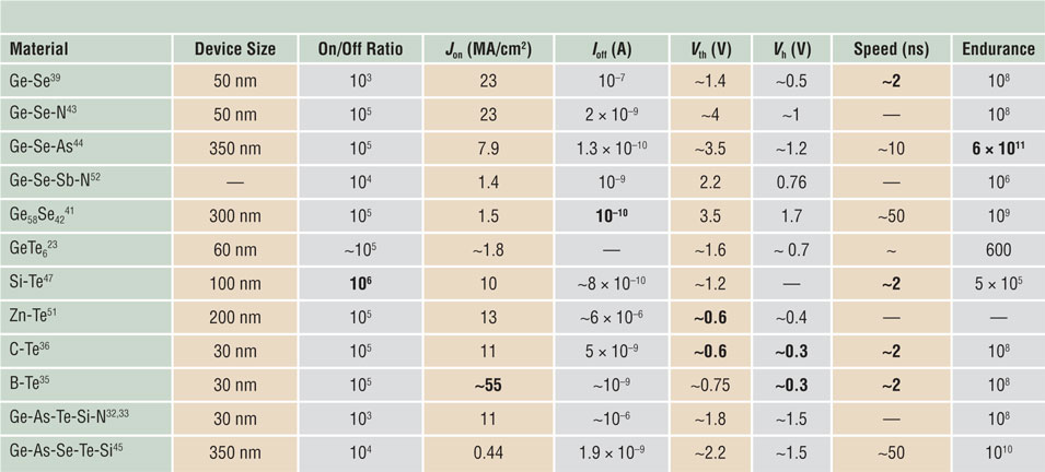
* Bold items highlight the best performances among these devices.
Se-based OTSs, as shown in Table I, typically present MA/cmReference Zhu2-scale J on, although a J on >20 MA/cm2 was also reported for undoped and N-doped Ge-Se OTSs.Reference Govoreanu, Donadio, Opsomer, Devulder, Afanas’ev, Witters, Clima, Avasarala, Redolfi, Kundu, Richard, Tsvetanova, Pourtois, Detavernier, Goux and Kar39,Reference Avasarala, Donadio, Witters, Opsomer, Govoreanu, Fantini, Clima, Oh, Kundu, Devulder, van der Veen, Van Houdt, Heyns, Goux and Kar43 Remarkably, they show long device lifetimes of >6 × 10¹¹ cycles for As-doped Ge-Se OTS.Reference Cheng, Chien, Kuo, Yeh, Gignac, Kim, Lai, Lin, Bruce, Lavoie, Cheng, Ray, Lee, Carta, Yang, Lee, Ho, BrightSky and Lung44 Moreover, the ultrahigh amorphous resistance, Se-based OTS is also characterized by low I off of ∼0.1 nA for Ge58Se42 and As-doped Ge-Se OTSs.Reference Navarro, Verdy, Castellani, Bourgeois, Sousa, Molas, Bernard, Sabbione, Noé, Garrione, Fellouh and Perniola41,Reference Cheng, Chien, Kuo, Yeh, Gignac, Kim, Lai, Lin, Bruce, Lavoie, Cheng, Ray, Lee, Carta, Yang, Lee, Ho, BrightSky and Lung44 For OTS with the same material, varying J on and selectivities were reported, which may be due to different cell structures, electrode sizes, and fabrication processes.Reference Verdy, Navarro, Bernard, Chevalliez, Castellani, Nolot, Garrione, Noé, Bourgeois, Sousa, Cyrille and Nowak48–Reference Verdy, Navarro, Bernard, Noé, Licitra, Bourgeois, Garrione, Cyrille, Sousa and Nowak52
Figure 3 shows the scalability of J on for a Ge-As-Te-Si-N-based OTS, as reported by Lee et al. Reference Lee, Lee, Kim, Choi, Park, Kim, Cha, Chung, Yoo and Kim32 Bez reported that for a 500 × 500 nm2 cell, a J on of 0.039 MA/cm2 was obtained, 10 times smaller than that required to operate the phase-change memory cell.Reference Bez53 Fortunately, the J on of the OTS exponentially increases as the device size shrinks. Although similar scaling behavior of current density was found for operating a phase-change memory cell, it increased much slower than that observed for OTS. As the device shrinks to 20 × 20 nm2, the J on of the OTS is expected to reach 22 MA/cm2,Reference Lee, Lee, Kim, Choi, Park, Kim, Cha, Chung, Yoo and Kim32 sufficient for programming the PCM cell.
Scalability of current densities with device size provided by GeAsTeSiN-based ovonic threshold switching (OTS)Reference Lee, Lee, Kim, Choi, Park, Kim, Cha, Chung, Yoo and Kim32 and current densities required for operating GeSbTe-based phase-change memory.Reference Bez53

Potential switching mechanism
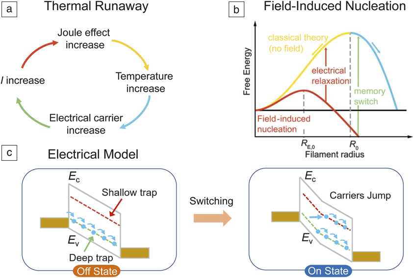
Although more and more OTS materials are being proposed, the inherent mechanism remains unclear. In the past half of a century, many models have been proposed to explain this phenomenon. Among them, the representative ones are thermal runaway, field-induced nucleation, and pure electronic models, as shown in Figure 4.
Three representative models to explain the ovonic threshold switching (OTS) phenomena: (a) thermal runaway,Reference Kroll54,Reference Kroll55 (b) field-induced nucleation,Reference Karpov, Kryukov, Savransky and Parpov57,Reference Karpov, Kryukov, Karpov and Mitra58 and (c) pure electrical phenomenon (yellow bars represent metal electrode).Reference Ielmini and Zhang66 Note: R E,0, critical size of nuclei induced by electric field; R 0, critical size of nuclei induced by thermal energy; E v, valence band; E c, conduction band.

The thermal runaway model, illustrated in Figure 4a, was first described by Kroll et al. in the 1970s.Reference Kroll54,Reference Kroll55 With increasing applied voltage, the current passing through the OTS cell increases. As a result, the induced Joule effect increases the temperature of the chalcogenide film, which further triggers more carriers. When the temperature rises sufficiently, a positive feedback switches on and the conductivity exponentially increases. Once the voltage reaches V th, the voltage subsequently decreases in order to maintain a high current density, resulting in the threshold switching. However, this model was greatly challenged by disagreement with the experimental conductivity-temperature relationship and the absence of negative-resistance behavior in simulations.Reference Kaplan and Adler56
Karpov et al. proposedReference Karpov, Kryukov, Savransky and Parpov57,Reference Karpov, Kryukov, Karpov and Mitra58 the field-induced nucleation model in 2007, based on the classical nucleation theory, as illustrated in Figure 4b. According to classical nucleation theory,Reference Zhu, Xia, Song, Cheng, Wu, Rao, Song, Wang, Lu and Feng59 the crystal growth process only take place after the nuclei exceed a critical size (R 0). Under an applied strong electrical field, subcritical nuclei form heterogeneously at the chalcogenide/electrode interface, reducing the device conductivity.Reference Karpov, Kryukov, Savransky and Parpov57 Nevertheless, these unstable subcritical nuclei will disappear when the electrical field is removed. This results in the transient nature of the OTS and the relaxation from a low-resistance to high-resistance state (Figure 1f). In contrast, if the electrical field is maintained, these subcritical nuclei develop into stable supercritical ones, even after the field is removed. As the crystalline filament is formed by the growth of these supercritical nuclei, the cell freezes in the highly conductive crystalline state, inducing the OMS behavior seen in Figure 1e.Reference Menzel, Bottger, Wimmer and Salinga60 The field-induced nucleation model predicts the experimentally observed V th–temperature relationship and switching delay time. Yet, the poor conductivity of crystalline OTS material when compared to the amorphous state, observed in GeSe, raises questions about this mechanism.Reference Ren, Zhu, Song, Lv, Xia, Wang, Lu, Ji and Song61
The electronic model can be tracked back to Kaplan and Adler’s work published in 1971;Reference Kaplan and Adler56 they noticed that a pure thermal model could not achieve negative differential resistance observed in OTS. In 1980, Adler et al. described the threshold switching effect as an interaction of charge-carrier generation and recombination mechanisms.Reference Adler, Shur, Silver and Ovshinsky62 In this model, lone-pair-induced traps above the valence band mobility play a critical role in the conductivity. More specifically, under an applied low electrical field, the field-induced carriers are captured by these traps, which leads to low conductivity. Under a strong field, the generation mechanism dominates, and threshold switching occurs, as all of the traps are filled so that the carriers can move freely. A current filament formed by these carriers leads to an amorphous on-state. As long as any filament remains, only a voltage above V hold is required to resuscitate the on-state. Upon further decreasing the voltage, the recombination mechanism dominates again and the filament disappears, resulting in the transition to the amorphous off-state.Reference Czubatyj and Hudgens63 Pirovano et al.Reference Pirovano, Lacaita, Benvenuti, Pellizzer and Bez64 and Redaelli et al.Reference Redaelli, Pirovno, Benvenuti and Lacaita65 reformulated Adler’s model after 2000, incorporating impact ionization from the charge carriers.
Ielmini et al., in their work, differed from Adler’s model and considered how traps play a positive effect on the conductivityReference Ielmini and Zhang66 (Figure 4c). Under a stronger field, carriers can jump from deep trap states into shallow trap states through thermal emission or tunneling processes. The energy of the excited carriers can be shared among neighboring ones, which causes a nonequilibrium distribution of carriers and nonuniform electric-field distribution. When sufficient carriers are excited into shallow trap states, the threshold switching behavior appears.Reference Menzel, Bottger, Wimmer and Salinga60 Ielmini’s model successfully accounts for the complete current–voltage relationship, which has been widely accepted. Clima et al. recently proved using first-principles simulations that an electric field can promote carrier repopulation, thereby increasing the conductivity of the OTS.Reference Clima, Govoreanu, Opsomer, Velea, Avasarala, Devulder, Shlyakhov, Donadio, Witters, Kundu, Goux, Afanasiev, Kar and Pourtois67
Conclusions
This article reviewed the evolution of emerging OTS materials after the successful integration of phase-change memory and OTS cells, and discussed their device performance. Continuous Te-based OTS materials have been reported, characterized by nanosecond-scale rapid switching speeds and >10 MA/cm2 large on current density. Another class of material is Ge-Se-based alloys, often doped with N, Sb, and As. They have gained much attention in recent years owing to good thermal stability, low leakage current and good endurances. As they can provide the high current densities required for programming conventional phase-change memory cells, current OTS cells have the capability of driving phase-change memory cells as the cell size shrinks to 20 nm.
Finally, we revisited the underlying physical mechanisms for the OTS phenomenon, including thermal runaway, field-induced nucleation as well as generation/recombination of charge carriers. It is generally accepted that the threshold switching is a purely electronic process, which seems to be well explained using Ielmini’s model. Even so, a clear and full understanding of the threshold switching behavior is still needed to enable the design of better OTS for high-density 3D stackable phase-change memory application.
Acknowledgments
This work is supported by the National Key Research and Development Program of China (2017YFB0206101), the Strategic Priority Research Program of the Chinese Academy of Sciences (XDPB12), and the National Natural Science Foundation of China (61504157). M. Zhu acknowledges support by the Hundred Talents Program (Chinese Academy of Sciences) and Shanghai Pujiang Talent Program (18PJ1411100).

Min Zhu is currently an associate professor at the Shanghai Institute of Microsystem and Information Technology (SIMIT), China. He received his PhD degree from SIMIT, Chinese Academy of Sciences, in 2014, where he was an assistant researcher. He joined RWTH Aachen University, Germany, as a postdoctoral fellow from 2015 to 2017. His current research interests include phase-change memory and the ovonic threshold switch. Zhu can be reached by email at minzhu@mail.sim.ac.cn.

Kun Ren is currently a postdoctoral fellow at the Shanghai Institute of Microsystem and Information Technology (SIMIT), China. He received his PhD degree from SIMIT, Chinese Academy of Sciences, in 2014. He was a R&D engineer at KLA-Tencor. He then joined Hangzhou Dianzi University, China, as a lecturer in 2016. His current research interests include phase-change materials and ovonic threshold switch materials and structures. Ren can be reached by email at kun.ren.nick@outlook.com.

Zhitang Song joined the Shanghai Institute of Microsystem and Information Technology, Chinese Academy of Sciences, in 1998. He received his PhD degree from the Electronic Materials Research Laboratory, Xi’an Jiaotong University, China, in 1997. He was the director of the State Key Laboratory of Functional Materials for Informatics in China from 2014 to 2018. His research focuses on the development of phase-change memory. He cultivated and organized a 100-person high-level R&D team, integrating industry, university, and research. His current research interests include phase-change memory, selectors, and chemical mechanical polishing. Song can be reached by email at ztsong@mail.sim.ac.cn.