

I. INTRODUCTION
Radio frequency identification (RFID) systems in the ultra-high frequency (UHF) band is getting much interest in several service industries, purchasing and distribution logistics, goods flow systems and internet of things [Reference Finkenzeller1]. The UHF RFID system generally consists of the reader and the tag, and operates at the band of North and South America (902–928 MHz). The reader with a circularly polarized antenna sends a radio frequency (RF) signal to a tag and receives a backscattered signal from the tag. A typical UHF passive RFID tag is composed of an antenna and an IC chip, which must meet matching techniques and economic requirements. In many applications, most UHF RFID tags have to be attached on the various objects and surfaces, the tag antennas have size constraints and gain is also limited. It is well known that most dipole-type antennas are adopted for RFID tags and use various inductively feeding techniques, such as T-matched feed, loop coupled feed, and U-shaped feed, in order to obtain high inductive reactance of the tags. For size requirement, curved dipole and meandering structures have been commonly used to reduce the length of the tag antenna [Reference Rao, Nikitin and Lam2–Reference Chen, Lin and Chen8]. Recently, a ground plane mode is proposed to overcome a bandwidth limitation. It is shown that the structure is formed by a small coupling patch near the system ground plane and the ground plane modes through the coupling patch with wideband matching circuits are excited [Reference Andujar and Anguera9, Reference Lin and Wong10]. It is well known that the electric coupled feeding method needs to apply a coupling element close to the maximum electric field of the ground plane, as the coupling patch in the configurations located at the end of the ground plane. Additionally, to obtain the optimal coupling between the patch and ground plane and do not arbitrarily reduce the antenna size, that a magnetic coupling feeding method dealing with size limitation have appeared in the literature [Reference Zhang, Liu, Kim and Kim11, Reference Liu, Lee, Kim and Kim12]. In those antennas, a slot with capacitors and inductors loaded is embedded at the center of the ground plane and close to the maximum current distribution of the ground plane. In that case, by tuning the ratio of the capacitor to the inductor can achieves a good impedance match and cannot changes the size of ground plane.
As known that the antenna gain and complex conjugate impedance match between the antenna and tag chip can be significantly affected the tag antenna properties. However, the inductive reactance of the tag antenna should be conjugate match with the capacitive reactance of the tag chip. In this paper, a magnetic coupling feed for exciting the dipole-type current mode of the ground plane is proposed. The proposed tag antenna consists of a simple rectangular ground plane and a resonant open-slot exciter embedded in the center of the ground plane. The resonant open-slot will be designed to have a total length of about quarter wavelength of a frequency in the operating band [Reference Wang and Chung13]. Thus, the currents flowing around the perimeter of the open-slot can be generated, which produces magnetic flux to excite the dipole-type current mode of the ground plane. The gain of the ground radiator is about 2 dBi as the value of the conventional dipole antenna. Detailed design mechanism of the proposed antenna is presented, and major parameters study of this antenna is also described in this paper.
II. ANTENNA DESIGN
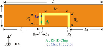
Figure 1 shows the structure of the proposed tag antenna, in which a rectangular ground plane with an open-slot embedded in the center of the ground plane, is printed on an FR4 substrate (L × W mm2) with thickness of 0.4 mm and relative permittivity 4.4. The open-slot structure is designed to an inverted-U shape with the fixed width (g 2), and the lengths of three parts of the open-slot are denoted W 1, L 2, and W 2, respectively. In this case, the open-slot is used as a resonated exciter, and the resonant length of the open-slot needs to be about quarter wavelength of 925 MHz. For exciting this resonating open-slot, an inductor L c and a tag chip are loaded in series for impedance matching. A vertical slot (W 1 × g 1 mm2) is etched in parallel to the left arm of the open-slot, which uses an inductor and a tag chip for connection. The tag chip is fed using an Alien Higgs-4 chip [14] at the bottom part of the vertical slot. The given input impedance of the chip is 8−j149 Ω at 925 MHz, and its threshold power sensitivity is about −19.5 dBm over 902–928 MHz band. Additionally, the position of the exciter, L 1, is placed at the left-end of the tag antenna.
Configuration of the proposed tag antenna.

Most commercial tag antennas are designed to dipole-like types, caused of its simplicity and easy fabrications. In this study, the required resonant feeding structure (open-slot exciter) needs to excite the ground plane for a radiator. Furthermore, by adjusting the lengths of the ground plane can control the resonant frequencies and antenna gain. The optimized parameters of the proposed antenna obtained by HFSS version 14 [15] are given in Table 1.
Parameters of the proposed antenna.

III. PARAMETRIC STUDIES AND OPTIMIZATION
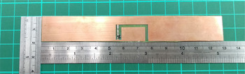
For achieving optimum antenna performance, a parametric study using the commercial software (HFSS) is carried out to investigate the characteristics of the tag antenna. To validate our design mechanism, an antenna prototype was fabricated and its photo is shown in Fig. 2.
Photograph of the fabricated antenna prototype.

It should be noted that the performance of RFID tag antenna is strongly affected by the frequency-dependent complex impedance depicted by the tag chip. Generally, RFID tags have been designed and need the chip impedance be known in advance. Thus, the resistance and reactance of the chip swept by a vector network analyzer from 800 to 1000 MHz were measured by the method in [Reference Chen, Yeh, Lin, Pan and Chang16] and then the optimized tag antenna needs to accommodate the design requirements. In this design that the tag antenna impedance should be conjugate matched correctly to the Alien chip impedance that is known to have Z a = 8 + j149 Ω at 925 MHz.
A) New concept of operating mechanism and open-slot exciter
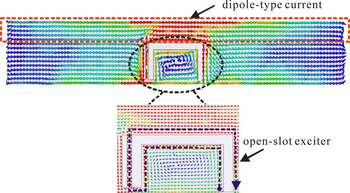
To validate this operating mechanism, the simulated vector current distribution on the proposed antenna is shown in Fig. 3. It can be seen that the dipole-type current flow on the ground plane is excited strongly by the open-slot exciter using magnetic coupled feeding mechanism. The mechanism is based on embedding an open-slot resonator at the center of the ground plane where the maximum magnetic field takes place. As seen that an open-loop current distribution (black dashed line) is generated around the open-slot exciter, which can produces magnetic flux to induce the dipole-type current mode of the ground plane by using the Ampere's circuital law. In this study, the total resonant length of the open-slot exciter is about 83 mm (black dashed line) which is about 0.256 λ0 at 925 MHz. For the conjugate match with the capacitive reactance of the tag chip, a series chip inductor (L c ) with inductive reactance is loaded in the open-slot exciter. In addition, the vector current flows in one direction along the ground plane, which is similar to the current flowing of the conventional half-wavelength dipole antenna. Thus, the total resonant length of dipole-type current mode is about 130 mm (red dashed line) which is about 0.51 λ g at 925 MHz, and λ g is the guided wavelength in the dielectric substrate (ε r ) as follows,
 $$\lambda _g = \lambda _0 \sqrt {\displaystyle{{1 + \varepsilon _r} \over {2\varepsilon _r}}}. $$
Simulated vector current distribution at 925 MHz for the proposed antenna.

B) Effects of the loaded inductor (L c )
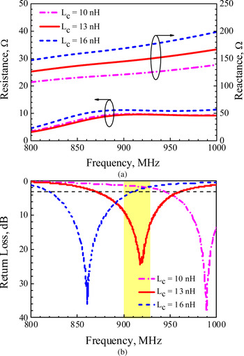
In order to achieve optimized conjugate match, the inductor loaded in the open-slot exciter shows significant importance. The values of inductor are varied to control the reactive match, and the simulated impedance and return loss are shown as in Fig. 4. Typically, the resistance and reactance of a dipole antenna varies depending on the total length and width of the radiator for the same structure and material. It is clear from Fig. 4(a) that the larger inductance obtains the higher input reactance and slightly changes the input resistance. The resonant frequency is determined by the inductor (L c ), shown as Fig. 4(b). It is found that the resonant frequency varies from 1000 to 860 MHz as L c is changed from 10 to 16 nH, the reason is that a well-matched impedance for each resonant frequency can be achieved by adjusting an appropriate inductance of L c . Therefore, a simple inductor loaded in the exciter could be completely adequate to match the capacitance of the chip. In the present design, the results show that the input resistance and reactance is matched to the chip impedance at 925 MHz as L c = 13 nH.
Simulation results for varying inductor values (L c ) for (a) input impedance and (b) return loss.

C) Effects of length (L) and width (W) of the antenna
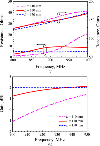
It is known that at different frequency, the impedance and realized peak gain of the tag antenna shows significant variations. Fig. 5 shows the simulated impedance and peak gain for the length L varied from 110 to 150 mm. Small variations of the reactance and large variations of the resistance are seen in Fig. 5(a). In Fig. 5(b), the peak gain is about 1.8–2.1 dBi at the desired frequency 925 MHz when the length is greater than 130 mm (0.51 λ g), and the gain is the same as a conventional dipole antenna. Also, it can be seen that the peak gain decreases when the length L = 110 mm, which is due to the mismatch of the input impedance. Additionally, the resonant frequency shifted to higher frequency with a relatively large gain is owing to the decreased resonant length L. As discussed, the resonant length L of 130 mm is selected to achieve optimal gain and size reduction.
Simulation results for varying lengths (L) for (a) input impedance and (b) peak gain.

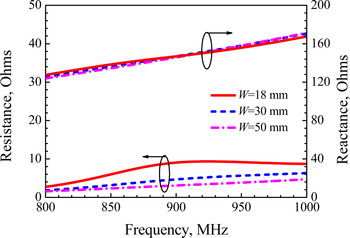
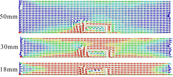
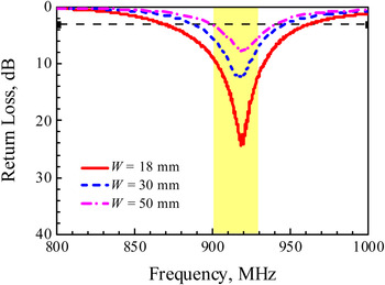
Effects of the width on the tag antenna's operating bands are also evaluated. Other parameters of the proposed antenna are the same as in Table 1. In Fig. 6, by varying the widths of the tag antenna, W, the input resistance decreases as W increases, but little effect on the reactance. The resistance decreasing is owing to the wider width, because a wider width can make the excited current distribution become smoother on the radiator and resulting in a lower resistance. The excited current distributions at 925 MHz for varying widths (W) are also shown in Fig. 7. As discussed, the results indicate that the width (W) and length (L) of the proposed antenna can effectively control the input resistance and reactance, respectively. Figure 8 shows the return loss for different widths. It is observed that the input resistance and reactance is matched with the chip impedance at 925 MHz as W = 18 mm.
Simulated input impedance for different widths (W).

Simulated current distributions at 925 MHz for different widths (W).

Simulated return loss for different widths (W).

D) Effects of the location of the open-slot exciter
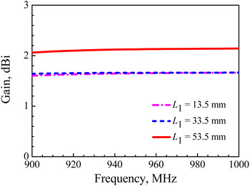
To demonstrate the optimal magnetic coupling between the open-slot exciter and antenna radiator, the exciter can then be adjusted the locations to achieve a higher gain. Figure 9 shows the simulated antenna gain for different positions of the exciter, L 1. In this simulation, the length of antenna (L) is fixed to 150 mm, owing to its smooth gain across the operating band, shown in Fig. 5. The antenna gain has maximum values of 2.1 dBi when the exciter is located at the center of the antenna (L 1 = 53.5 mm). As the exciter shifts to the left end of the antenna with weak current distribution, the gain decreases and is about 1.6 dBi as L 1 decreases. The results show that the maximum current distribution is excited at the center of the antenna radiator, which produces the magnetic flux wrapped around the currents and couples in phase with the magnetic field of the open-slot to obtain a maximum gain.
Simulated peak gain with varying the positions of the exciter (L 1).

IV. EXPERIMENTAL RESULTS AND DISCUSSIONS
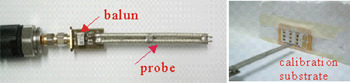
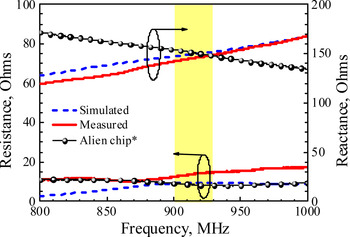
The prototype antenna is designed for Alien Higgs-4 chip, whose input impedance is 8−j149 Ω and the power sensitivity is −19.5 dBm at 925 MHz. The physical dimension of the proposed antenna with an open-slot exciter is adjusted to obtain impedance that provides a conjugate match of the impedance of the chip, shown in Fig. 1. The dimensions of the optimized antenna are listed in Table 1 and the photo of the prototype antenna is also shown in Fig. 2. The measurement was performed by using an Agilent N5071C vector network analyzer, connected to a single-ended probe equipped with a balun transform, to measure the impedance of the tag antenna [15]. The photographs of a probe equipped with a balun transform and its calibration substrate (Agilent 1NB7-8474) are shown in Fig. 10. The measured and simulated input impedance of the prototype are in good agreement and shown in Fig. 11. The measured and simulated input impedance of the proposed antenna in free space at 925 MHz are 15 + j148 Ω and 9 + j151 Ω, respectively. It can be seen that the measured and simulated input impedance at 902–928 MHz is very close to the conjugate impedance of chip, which will obtain a better impedance bandwidth. However, to achieve a good performance of the tag, the antenna impedance and chip impedance should be good matched to get a maximum power transfer between the antenna and the chip. The power reflection coefficient Γ, return loss and power transmission coefficient τ are defined as [Reference Finkenzeller1, Reference Rao, Nikitin and Lam2]
 $$\eqalign{& \Gamma = \displaystyle{{Z_a - Z_c^{\ast}} \over {Z_a + Z_c}} {\rm, Return \; Loss =} - {\!20 \; {\rm log}}\left \vert \Gamma \right \vert, \cr & \tau = 1 - \left \vert \Gamma \right \vert ^2 = \displaystyle{{4R_a R_c} \over {\left \vert {Z_a + Z_c} \right \vert ^2}}, \; \; 0 \le \tau \le 1,}$$
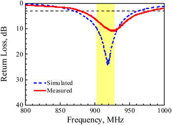
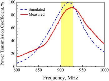
where Z a = R a + jX a represents the tag antenna impedance, and Z c = R c + jX c represents the complex chip impedance. The measured and simulated return loss and power transmission coefficient of the proposed antenna are shown in Figs 12 and 13. For the realization of impedance matching between the antenna and chip, a half-power bandwidth (3-dB return loss) was adopted in UHF RFID system. In Fig. 12, it can be observed that the measured 3-dB return loss bandwidth is 90 MHz (870–960 MHz). The measured power transmission coefficient (PTC) value is also achieved from 80 to 90% at the operating band depicted in Fig. 13. As we know that the minimum power transmission coefficient value is greater than 60% at the operating frequency, indicating the impedance match between the antenna and chip is acceptable. However, the measured results in general agree well with the simulated ones as observed in Figs 12 and 13.
Photographs of a probe equipped with a balun transform and its calibration substrate.

Measured and simulated input impedance.

Measured and simulated return loss.

Measured and simulated power transmission coefficient.

To verify the performance of the tag, the read range is studied. The read range is the maximum distance that the tag can send a response data back to the reader. The read range r was calculated using Friis free-space formula [Reference Finkenzeller1, Reference Rao, Nikitin and Lam2] as
 $$r = \displaystyle{\lambda \over {4\pi}} \sqrt {\displaystyle{{P_t G_t G_r \tau} \over {P_{th}}}},$$
 $$P_{tag} = \displaystyle{{P_{th}} \over {G_r \tau}},$$
where λ is the operating wavelength, P t and G t represent the transmitted power and gain of the reader antenna, respectively. G r represents the simulation peak gain of the tag antenna, P th represents the minimum threshold power of chip, and τ is the power transmission coefficient given by (1). Tag sensitivity (P tag ) denotes the minimum transmit power that is needed to activate the tag as a function of transmit frequency.
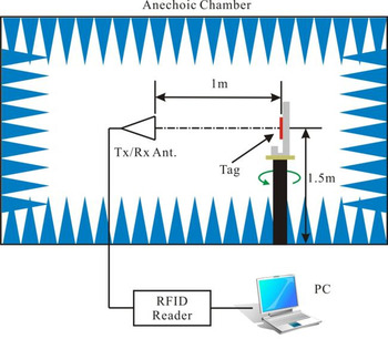
In order to predict and verify the tag performance, the experimental setup about the maximum read range for the fabricated tag was carried out in an anechoic chamber, as shown in Fig. 14. The RFID measurement system comprises a computer, a reader controller (Favite FS-GM-201) [17], a reader circularly polarized (CP) antenna, and an oriented fabricated tag. The measurement followed the test method of [18]; r is the distance between the tag and the reader antenna and is fixed at 1 m, G t = 6.0 dBi and P t is a variable transmitted power with a cable loss calibration. In this study, we set the reader transmitting power P t to the lowest power and then gradually increase it until the reader can read the tag response for more than 80% of 20 reads. As a result, the tag sensitivity P tag is measured at each frequency for the x–z and y–z planes, and the relative measured maximum read range of the fabricated tag obtained from the Friis formula (2) is more than about 9 m in x–z and y–z planes, which is tested for an RFID reader with 4.0-W of effective isotropic radiated power (EIRP).
RFID tag read range measurement using anechoic chamber.

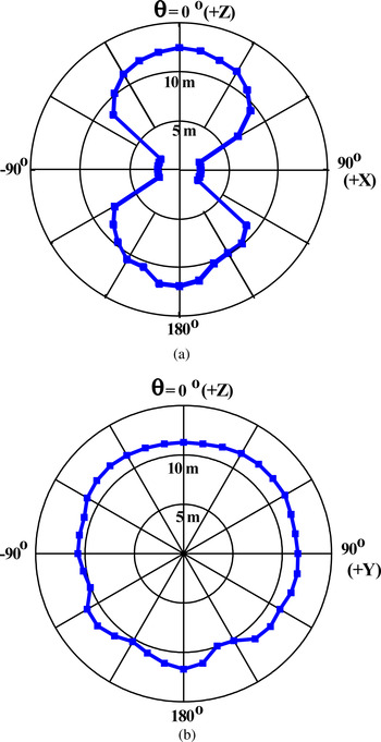
To determine the tag angular sensitivity patterns, the tag attached on the rotary foam is rotated at the x–z and y–z planes with a 10° step from 0° to 360° at 925 MHz. The measured tag angular sensitivity pattern presents a good omni-directional pattern in the y–z plane and also the pattern in the x–z plane is similar to 8-figure, which are consistent with those of a typical dipole antenna, as shown in Fig. 15.
Measured tag angular sensitivity patterns of the proposed tag antenna at 925 MHz. (a) x–z plane (b) y–z plane.

V. CONCLUSION
A novel design process and simple matching mechanism for a ground radiator with open-slot exciter is fabricated and measured. It should be mentioned that the ground radiator is a half-wavelength dipole-like antenna and the open-slot exciter is a quarter-wavelength resonator. The proposed antenna can achieve easily impedance match by tuning an inductor and obtain relatively high gain. Also, the measured tag angular sensitivity patterns resembled those of λ/2 dipole. Measured maximum read distance can reach more than 9 m with an EIRP set to 4.0-W.
ACKNOWLEDGEMENT
This work was supported by the National Science Council of Taiwan under Contract NSC100-2221-E-151-054-MY3.
 Yi-Fang Lin received the B.S. degree in physics from National Tsing Hua University, Hsinchu, Taiwan in 1993, both the M.S. degree in Institute of Electro-Optical Engineering and the Ph.D. degree in electrical engineering, from National Sun Yat-Sen University, Kaohsiung, Taiwan, in 1995, and 1998, respectively. Since 2000 she has been with the Institute of Photonics and Communications at National Kaohsiung University of Applied Sciences, Kaohsiung, Taiwan, where she became a Professor in 2013. Her current research interests include microstrip antennas, dielectric resonator antennas, and small antennas design.
 Ming-Jui Chang was born in Changhua, Taiwan, in 1987. He received the B.S. degree in computer and communication engineering from Shu Te University, Kaohsiung, Taiwan, in 2009, and the M.S. degree at the same university in 2011. He is now working toward the Ph.D. degree from electronic engineering at National Kaohsiung University of Applied Sciences. His main research interests are in muti-band antenna design for metal-casing devices, mobile devices with the MIMO antennas, and RFID applications.
 Hua-Ming Chen (M'98-SM'06) received the B.S. degree in physics from National Tsing Hua University, Hsinchu, Taiwan, the M.S. degree in Institute of Electro-Optics from National Chiao Tung University, Hsinchu, Taiwan, and the Ph.D. degree in electrical engineering from National Sun Yat-Sen University, Kaohsiung, Taiwan, in 1983, 1987, and 1996, respectively. Since 1988 he has been with the Institute of Photonics and Communications at National Kaohsiung University of Applied Sciences, Kaohsiung, Taiwan, where he became a Professor in 2001. He also served as Director of Institute of Photonics and Communications at the same university from 2005 to 2008. He has published more than 110 journal and conference papers and takes out 20 patents on antenna design. Several of his antenna designs have been licensed to industry for production. His current research interests include antennas for smart connected devices, dielectric resonator antennas, RFID antennas and microwave filter design. He was elected as a President of the Institute of Antennas Engineers of Taiwan (IAET) in 2010–2012. He was also elected as Chair of IEEE AP-S Tainan Chapter in 2009–2010 and has received IEEE 2011 Best Chapter Award. He served as Trustees of IEEE Tainan Section (2010–2011) and Chinese Microwave Association (2009–2011). He also served as a Publications Committee Chair of ISAP 2014, International Technical Program Committee member of IEEE AEM2C 2010 and IEEE iWEM 2011 in Taiwan.
 Shih-Ting Huang was born in Kaohsiung, Taiwan, in 1990. He received the M.S. degree in National Kaohsiung University of Applied Sciences, Kaohsiung, Taiwan in 2014. He is currently working on design of RFID tag antenna at school. His main research interests are in circularly polarized operation and RFID tag antenna mounted on metal material.