I. INTRODUCTION
Since a couple of years, electronic applications offering to consumers a wireless electrical charging way instead of a classical wired one are more and more present in the market [Reference Ryan1]. Wirelessly powering nomad objects (smart phones, cellular phone, personal computer, space-based navigation system, etc.) seems to be a very smart and ergonomic solution [Reference Chen, Kawasaki and Carvalho2]. To implement a wireless power system there are basically three approaches: reactive near-field coupling (inductive and resonant) [Reference Flynn and Fotopoulou3, Reference Mayordomo, Dräger, Spies, Bernhard and Pflaum4], far-field directive power beaming [Reference Dickinson5], and far-field nondirective power transfer [Reference Popovic6].
A classical wireless power transfer (WPT) system employing the reactive near field coupling is illustrated in Fig. 1. The power transfer between the transmitter (Tx) and the receiver (Rx) is made by using coupled coils.
Classical near field WPT system.

The coils are commonly realized using two technologies: Litz wire or printed circuit board (PCB).
Litz coils consist of many thin wire strands, individually insulated and twisted or woven together in order to reduce the losses. Mainly from low frequency applications, Litz coils have usually low losses and thus a very good quality factor but this technology is more expensive than PCB one. PCB coils are manufactured by printing metallic traces with selected shapes directly on the PCB [Reference Tang, (Ron) Hui and Shu-Hung Chung7]. So several models and shapes can be easily manufactured, on multiple layers. The major advantages are an easy fabrication process, a high diversity of shapes or disposition and a lower price compared with Litz coils. The main drawbacks are the low quality factor and thermal issues.
Several recent papers [Reference Su, Liu, Kwan Lee and (Ron) Hui8–Reference Jow and Ghovanloo12] addressed the design of PCB coils showing their strong potential for WPT applications. The performances of the PCB coils can be improved by using a soft magnetic material (ferrite) strategically placed in the vicinity of the coil [Reference Wielandt and Stevens13]. By following specific design rules, a good quality factor and power efficiency (called link efficiency) could be achieved.
This paper addresses an effective and accurate modeling technique of PCB coils for WPT purpose by using intensive full wave electromagnetic simulations (using FEKO software (https://www.feko.info/)). It will focus on coils using the PCB technology operating at different frequencies (100–1000 kHz) because this technology has the most potential of improvement.
Section II deals with the theoretical equations used to describe the performances of PCB coils.
The design methodology adopted for the optimization of the PCB coils performances is presented in Section III while the impact of the ferrite is modeled in Section IV. Based on the results obtained by using intensive electromagnetic simulations, parametric analyses were performed. The emanated conclusions allow a better understanding of the impact of geometrical parameters of PCB coils and ferrite on the overall performances of WPT systems.
II. COUPLING FACTOR AND LINK EFFICIENCY
A) Coupling factor
The coupling between the two coils (Tx and Rx) used to implement an inductive WPT system is quantified by the so-called coupling factor. This factor depends on the geometric parameters of the coils, their relative position, and the distance between them. From a physical point of view the coupling factor (k) models the amount of magnetic flux exchanged between the Tx and Rx coils. It varies from 0 (coils completely decoupled and independent of each other) to 1 (coils totally coupled when all the flux generated by the Tx coil is transmitted to the Rx coil).
The coupling factor (k) is defined by the following equation:
 $$k = \displaystyle{M \over {\sqrt {Lp \times Ls}}}, $$
where M represents the mutual inductance between the primary (Tx) and secondary (Rx) coils while Lp and Ls are the Tx and Rx coils’ inductances.
B) Link efficiency
A key parameter for any power electronic system and particularly for WPT systems is the efficiency [Reference Pinuela, Yates, Lucyszyn and Mitcheson14]. In our case, the link efficiency measures the quantity of power transferred from the Tx to the Rx coil and varies between 0 and 1. Theoretical link efficiency [Reference Ko, Liang and Fung15] can be defined as:
 $$\; {h_{link}} = \; \displaystyle{{k^2{Q_{Tx\;}} {Q_{Rx}}} \over {(1 + \sqrt {(1 + {k^2}{Q_{Tx\;}} {Q_{Rx}})} )^2}},$$
where k is the coupling factor defined by (1), Q Tx , and Q Rx are, respectively, the quality factors of the Tx and Rx coils.
The coil's quality factor, representing the ratio of apparent power to power losses, is given by (3):
 $$Q_{Coil = {L \times w \over ESR}}, $$
where L is the value of the coil inductance, ω denotes the angular frequency of the AC current exciting the coil and ESR is the equivalent series resistance of the coil.
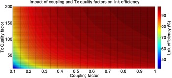
Figure 2 shows the impact of Q Tx and k factors on the link efficiency (for a typical Q Rx = 15).
Link efficiency formula in function of Tx quality factor and coupling factor (Q Rx = 15).

III. DESIGN METHODOLOGY AND OPTIMIZATION OF PCB COILS
A full wave electromagnetic simulation technique by using FEKO software was adopted.
This approach offers the possibility to model PCB coils with any shape, to take into account the use of a ferrite with arbitrary shapes and moreover to estimate the impact of other structures (e.g. NFC coils, GSM antenna, metallic traces, etc.) located near to the inductive coils used to implement the WPT function. This approach allows obtaining directly the magnetic field distribution as well as circuital parameters (inductance, resistance, quality factor, etc.).
The major drawback is the simulation time that can be excessive for complicated shapes. Nevertheless, this can be overcome by parallel computing (using a cluster). The results presented in this paper were obtained by using an 8 nodes (CPU cores) cluster.
Moreover FEKO software includes several numerical/hybrid methods (e.g. method of moments (MoM), finite element method (FEM)). These reasons justify the use of FEKO software for this electromagnetic modeling of PCB coils in a WPT purpose.
First, the impact of the PCB dielectric and the adopted meshing density was investigated on a reference coil. The correlation between the simulated and experimental results was checked and thus the adopted simulation methodology was validated. Meshing is a critical point in all electromagnetic simulations, defining how precisely Maxwell's equations are solved by using a numerical discretization of the geometry. FEKO software is based on the MoM and offers hybridization with other numerical methods (e.g. FEM).
For different meshing sizes, the simulated results were compared with the measured ones obtained by the characterization of a manufactured prototype. The validation of the simulation methodology is essential and the main goal was to validate an accurate modeling/simulation approach requiring reasonable computing time/resources needs.
In the second part, a parametric analysis of PCB coils was performed as function of the number of turns, the trace width, the gap (between traces) or the copper thickness. The selected structure for this parametric analysis is a one layer hollow spiral coil. The link efficiency was extracted for this model and evaluated with a specific Rx coil which is a model of the TPR1#A. This structure from the WPC specifications [16] consists of a coil made of Litz wire with a ferrite on its back. From these different parametric results, the configuration offering the best link efficiency will be used to characterize the impact of a piece of ferrite in Section IV.
A) Impact of the dielectric and meshing
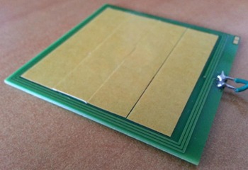
A reference PCB coil previously designed and manufactured for WPT applications at 6.78 MHz, available at the beginning of our work and represented in Fig. 3, was used to validate the proposed simulation methodology (brown parts are adhesive tape with no influence on the coil). This reference coil (RFC1) consists of a three turns 3364 mm2 square loop (outer side: 58 mm, strip width: 0.5 mm, gap between strips: 0.1 mm).
Prototype of the reference coil RFC1.

The adopted numerical method was MoM-volume equivalence principle (VEP) approach (https://www.feko.info/product-detail/numerical_methods/mom). The MoM technique is generally applicable to problems involving currents on metallic/dielectric electrically small structures. The main advantage is that the free space is not discretized thus leading in a reduction of the simulation time for the coupled coils. The double precision numerical format and the low frequency stabilization for MoM were activated.
Three modeling cases were studied and compared with measurement:
-
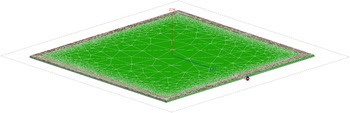
(i) Medium mesh model with substrate: the copper traces are placed above the cuboids representing the FR4 dielectric. On the considered frequencies (100 kHz – 1 MHz), the dielectric has a relative electric permittivity of 4.8 and a dielectric loss tangent of 0.017. As illustrated in Fig. 4, the PCB coil and dielectric volume are meshed with, respectively, 2713 triangles (used to mesh metallic surfaces) and 25 241 tetrahedra (used to mesh the dielectric volume). The simulation time was 16 h.
-
(ii) Coarse mesh model without substrate: the dielectric substrate is neglected and the copper traces are placed in free-space. A coarse mesh of 850 triangles was used. The simulation time was approximately 3 min.
-
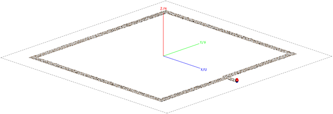
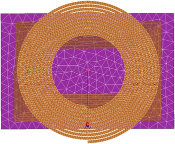
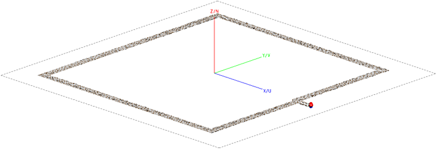
(iii) Fine mesh model without substrate: as shown in Fig. 5, the copper traces are placed in free space (the supporting FR4 substrate is not included in the model) and a fine mesh of 6200 triangles was used. The simulation time was 10 min.
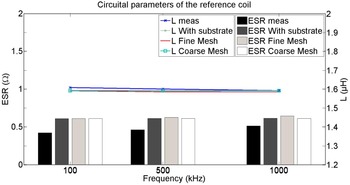
The inductance and equivalent series resistance (ESR) of the reference coil obtained for the three modeling approaches are illustrated in Fig. 6.
Simulation model (mesh) of the reference coil and dielectric FR-4.

Simulation model (mesh) of the reference coil alone.
Impact of the different modeling approaches for the reference coil: simulation results are compared with measurement ones.

The simulated ESR results are a little bit higher than measured ones, but the trend is respected. The small differences are due to the accuracy issues of the adopted simulation/model approach at such low frequencies (accuracy is quite better when the frequency increases) and to the non-modeling of small parts (e.g. connection pads). A good correlation between measurement and simulation was obtained for the inductance L.
Moreover, there are quasi no-differences between the simulated results obtained for the three cases (medium mesh density with dielectric, coarse mesh density without dielectric, and fine mesh without dielectric).
The results depicted in Fig. 6 demonstrate that:
-
(i) the dielectric can be neglected during the simulation (frequencies below 1 MHz). From a physical point of view this is true because the coupling mechanism between the inductive coils is done by the magnetic field and it is not impacted by the dielectric at such “low” frequencies. Consequently the copper traces of coils’ models were simulated without any substrate (FR4 dielectric);
-
(ii) the modeling of a PCB coil in the vacuum with a coarse meshing density gave accurate results with a reasonable simulation time and a moderate use of computing resources. This simulation configuration was finally adopted in our paper.
From the previous observations, the different models of PCB coils were simulated by using a moderate mesh density, in the vacuum and without any substrate to carry the copper traces. Thus we optimized the costs in terms of computing resources and simulation time.
B) Parametric analysis and optimization of PCB coils
Once the modeling approach validated, a basis coil was selected as a starting point for our analysis.
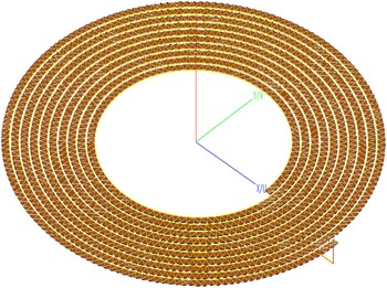
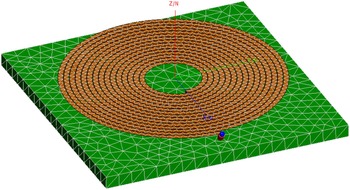
It consists of a hollow spiral coil (Fig. 7) with 10 turns, a trace width of 0.85 mm, a copper thickness of 35 µm, and a gap of 0.2 mm between turns for an inner radius of 10.5 mm. The inductance of this coil computed with Wheeler formula [Reference Wheeler17] is 4.04 µH, which is close to the simulated value (4.2 µH). Circuital parameters are extracted in order to obtain the quality factor of the coil.
View of the selected spiral hollow Tx coil used in our parametric studies.

As specified before, the coupling factor is obtained with the use of the Rx coil corresponding to the TPR1#A design, from WPC Low Power Specifications [18], which is centered and placed at a 5 mm distance of the Tx coil.
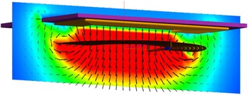
The Tx–Rx system is represented in Fig. 8 and the magnetic field distribution between Tx and Rx coils is illustrated in Fig. 9.
View of the previous Tx coil with the Rx coil for coupling factor and link efficiency evaluation.

View of the magnetic field generated for Tx–Rx coils system.

The impact of several parameters such as the width (w) and the thickness (t) of the copper traces, the gap (g) between them and the numbers of turns (n) on WPT performances was investigated. The analysis is performed at three chosen frequencies (100, 500, and 1000 kHz) commonly used for WPT systems.
For each case, circuital parameters (L and ESR) of the Tx coil as well as the coupling factor with the Rx coil were extracted from the electromagnetic simulation results and the link efficiency defined by (2) was computed. This link efficiency illustrates the WPT performances of the Tx coil, as seen in Section II.
1) Parametric analysis
A parametric analysis based on intensive electromagnetic simulation was performed in order to underline the impact of geometrical parameters of the Tx coil on the link efficiency of the adopted WPT system.
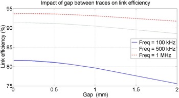
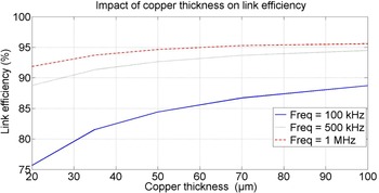
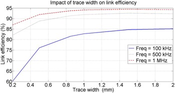
The results are depicted in Figs 10–12, respectively. For each case (figure), only one parameter was varied while others were kept constant.
Link efficiency as function of the gap between traces (number of turns n = 10 turns, trace width w = 0.85 mm, copper thickness t = 35 µm, and inner radius IR = 10.5 mm).

Link efficiency as function of copper thickness (n = 10 turns, w = 0.85 mm, g = 0.1 mm, and inner radius IR = 10.5 mm).

Link efficiency as function of trace width (n = 10 turns, t = 35 µm, g = 0.1 mm, inner radius, and IR = 10.5 mm).

We note that:
-
(i) -the link efficiency increases when the gap diminishes and when the copper thickness increases,
-
(ii) -the link efficiency increases also with the trace width but a limitation effect appears starting from w = 1.2 mm.
A form of logic is behind these results. When the gap between traces is reduced, the inductance increases (inner radius kept constant). So the quality factor and de facto the link efficiency rise.
The DC resistance of the Tx coil diminishes when the thickness and the width of traces rise. At such low frequencies, the DC resistance caused by the ohmic losses in the metallic (copper) traces is the major part of the total ESR (DC + AC) resistance.
2) Optimization of PCB coils
As presented before, the coupling factor depends on the inductance of the coils and the relative arrangement between Tx and Rx coils. For the investigated hollow spiral coils, the inductance is mainly influenced by the number of turns and the size of the inner/outer radius. The inductance is also impacted by the gap between the traces and their width. The previous parametric analysis demonstrated that a Tx hollow spiral coil having t ≥ 35 µm, w ≥ 0.8 mm, and g < 0.2 mm exhibits good link efficiency (in combination with the selected Rx coil) for frequencies below 1 MHz.
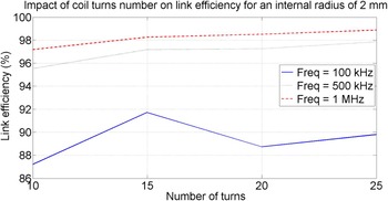
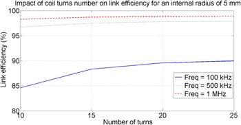
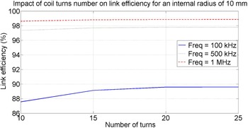
The impact of the inner/outer radius and the number of turns was not presented in the previous section. Thus Tx coils having inner radius IR = 2, IR = 5, and IR = 10 mm were investigated. The number of turns varies from 10 to 25. Figures 13–15 show the variation of the link efficiency for the selected inner radius values as function of the number of turns.
Link efficiency as function of turns number for IR = 2 mm (t = 70 µm, g = 0.1 mm, and w = 0.85 mm).

Link efficiency as function of turns number for IR = 5 mm (t = 70 µm, g = 0.1 mm, and w = 0.85 mm).

Link efficiency as function of turns number for IR = 10 mm (t = 70 µm, g = 0.1 mm, and w = 0.85 mm).

As general rules, the efficiency increases when the number of turns, the frequency, and the inner radius increase.
The value of IR = 5 mm (n > 15, t = 70 µm, g = 0.1 mm, and w = 0.85 mm) seems to be a good trade-off between link efficiency and the compactness. From a practical point of view the total surface of the PCB coils must be kept minimal because the available surface is limited or several PCB coils must be integrated in order to obtain a charging platform with a homogenous magnetic fields distribution.
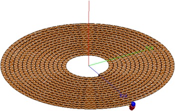
Based on the parametric analysis performed before (results depicted in Figs 10–15) we conclude that a Tx PCB hollow spiral coil with an interior radius of 5 mm, a turns number of 15, a copper thickness of 70 µm, a traces width of 1 mm, and a gap between them of 0.1 mm is an optimal design for our WPT system. By using this optimal design illustrated in Fig. 16, we can obtain a link efficiency varying from 88.3% (100 kHz) to 98.5% (1 MHz).
Model of the proposed Tx PCB hollow spiral coil allowing an efficiency of 98.5% at 1 MHz.

IV. IMPACT OF FERRITE ON WPT PERFORMANCES
As explained in Section I, some soft magnetic materials called ferrite can be used in a WPT system. By a strategic placement of a ferrite around the WPT coils, it is possible to influence the shape and intensity of the magnetic field and to meaningfully improve the WPT performances [Reference Ahuir19].
From a physical point of view the ferrite is characterized by its complex magnetic permeability [Reference Pramanik20]:
 $${\mu _m} = \; \mu ^{\prime} - j\mu ^{\prime \prime} = {\mu _0}{\mu _r}{e^{ - j{\delta _m}}}.$$
From this complex magnetic permeability can be derived the complex relative magnetic permeability (μ rm ) and the magnetic loss tangent (tanδ m ). These are defined by the following equations:
 $${\mu _{rm}} = \; \displaystyle{1 \over {{\mu _0}}}\left( {\mu ^{\prime} - \; j\mu ^{\prime \prime}} \right) = \mu _{rm}^{{\prime}} - j\mu _{rm}^{{\prime}{\prime}}, $$
where μ 0 is the vacuum magnetic permeability (μ 0 = 4π × 10−7 H.m−1)
 $$tan{\delta _m} = \; \displaystyle{{\mu ^{\prime \prime}} \over {\mu ^{\prime}}}. $$
The ferrite materials properly positioned in the vicinity of the Tx coil can focus the magnetic field in some directions. They can act as a “reflector” or a “shield” (useful for electronic circuits against unintentional electromagnetic emissions leading to dysfunctions). Usually, ferrite pieces are composed of Fe2O3XO where X is a divalent metal as cobalt, nickel, manganese or zinc.
A) Simulation and modeling approach
A square ferrite L7H [21] from the manufacturer TDK is placed behind the reference coil (RFC1) presented in Section III. The dimensions of the ferrite cuboid are 50 × 50 mm2. Three models using coarse (2405 tetrahedra), medium (6278 tetrahedra), and fine (13 652 tetrahedra) mesh densities were simulated. The coil is meshed with a coarse mesh density (863 triangles) and the MoM-VEP approach is employed to simulate the ferrite (simulation model represented in Figs 17 and 18). The double precision numerical format and the low frequency stabilization for MoM were activated as before.
Modeled reference coil with ferrite.

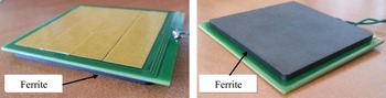
Prototyped reference coil (RFC1) with the ferrite positioned below (left: top view, right: bottom view).

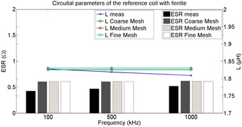
The circuital parameters extracted from experimental and simulation results are depicted in Fig. 19.
Impact of the different modeling approaches adopted for simulations of the RFC1 coil with a ferrite square positioned below.

A good correlation between measurements and simulations at different frequencies was obtained for the inductance and for the ESR. More, there are slight differences between the results obtained for different mesh. We can conclude that there is no need of fine mesh density and high computing resources to simulate a PCB coil with a ferrite at these frequencies.
Figure 19 can be compared with Fig. 6, to discuss the ferrite influence on the reference coil. For each considered frequency, the ESR is lightly higher with the ferrite while the inductance strongly increases. This behavior can be caused by a ferrite area smaller than the coil winding, a strong magnetic permeability, and a low magnetic loss tangent. The ferrite employed here presents a μ′ rm close to 800 and μ″ rm < 10.
B) Parametric analysis of ferrite's impact on WPT optimization
The ferrite impact will be investigated through geometric (area and distance to the coil) and magnetic (relative permeability) parameters.
The ferrite used in our model has the following standard parameters: area = 2500 mm2, thickness t = 2.5 mm, relative magnetic permeability μ′ rm = 800, and magnetic loss tangent tanδ m = 0.00125 (corresponding to a μ″ rm close to 1), and positioned at a distance of 2.5 mm below the PCB coil.
Identical to the previous prototyped ferrite, all these parameters are the starting/standard values of our parametric analysis.
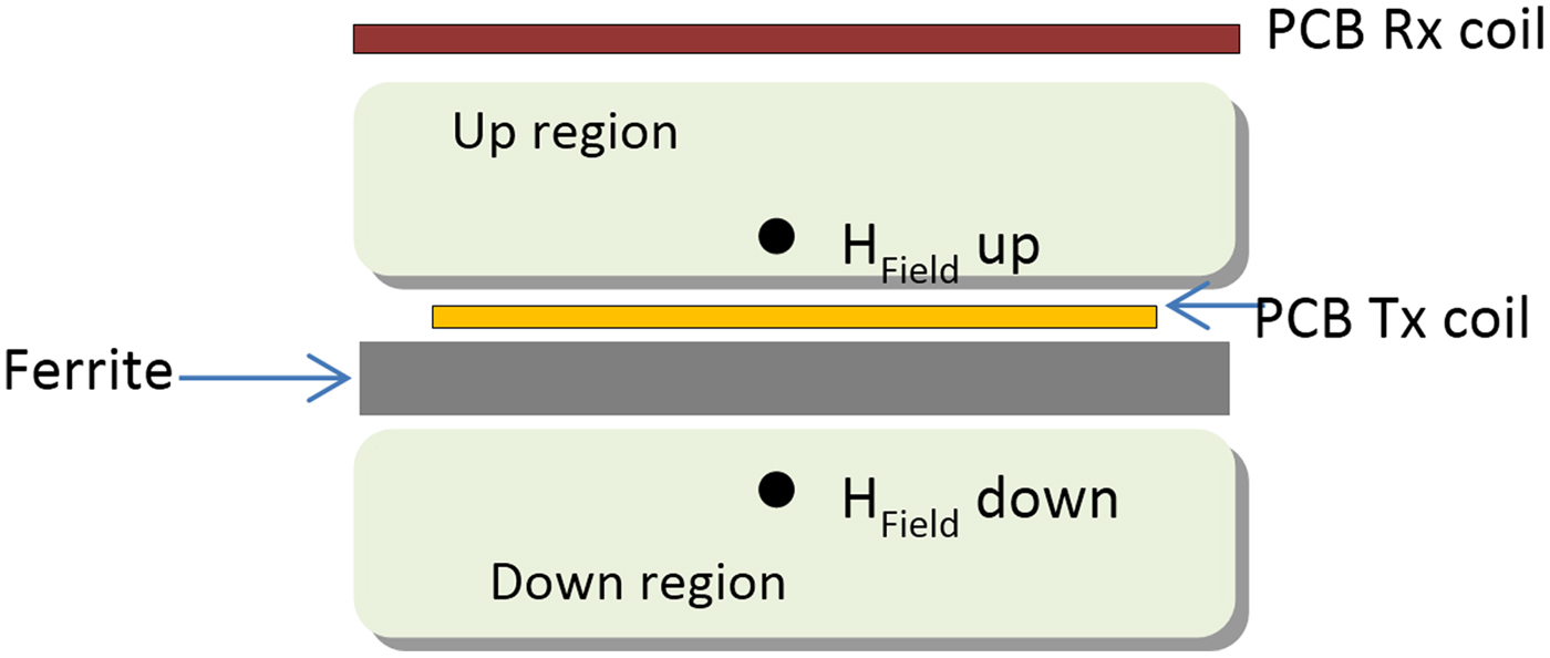
Once again, these parameters were varied one at a time to get an accurate picture of their impact on WPT performances. As the previous study, circuital parameters (L and ESR) of the Tx coil as well as the coupling factor with the Rx coil were extracted and the link efficiency was represented. To evaluate the effect of the ferrite on the magnetic field (H-Field), the notions of magnetic shielding and H-field enhancement are introduced (where only the Tx coil is considered and the Rx coil is not present within the modeling setup).
We define the magnetic shielding as the generated magnetic fields behind the coil with the ferrite normalized to the one without the ferrite, as shown by the following equation:
 $${H_{Shielding}}\left( \% \right) = \left \vert {1 - \displaystyle{{Hfield_{Down}^{with\; ferrite}} \over {Hfield_{Down}^{\scriptstyle{w \over o}\,ferrite}}}} \right \vert \times 100. $$
This ratio is computed at equivalent distances and locations in order to have a precise idea of ferrite shielding abilities.
The enhanced magnetic field is defined as the H-Field generated by the coil in the “up region” with the ferrite, normalized to the one without ferrite, as shown by the following equation:
 $${H_{Enhancement}}\left( \% \right) = \left \vert {1 - \displaystyle{{Hfield_{Up}^{with\; ferrite}} \over {Hfield_{Up}^{\scriptstyle{w \over o}\,ferrite}}}} \right \vert \times 100.$$
The two previous formulae are represented in absolute values in order to underline the (positive) impact of the ferrite on the coil performances.
These measurements are done at a distance of 1 mm above the coil for the “up region” and 1 mm behind the ferrite for the “down region”, and this on a centered location as illustrated in Fig. 20.
Definition of the “up” and “down” regions for the WPT system.

1) Results: geometric parameters variation
Geometrical parameters such as the distance between the ferrite and the Tx coil and the areas ratio (defined as the ratio between the area of the ferrite and the area of the PCB coil) are investigated.
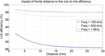
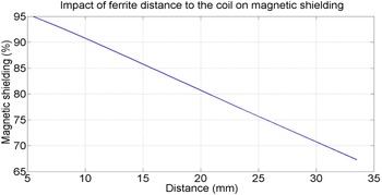
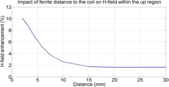
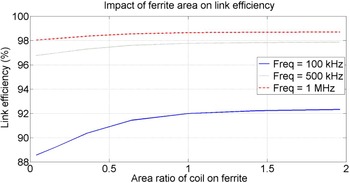
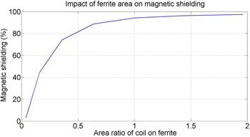
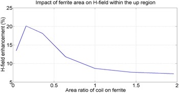
Figures 21–23 show the impact of the distance (between ferrite and Tx coil) on WPT performances whereas Figs 24–26 show the impact of the areas ratio between the Tx coil and ferrite.
Link efficiency as function of the distance between Tx coil and the ferrite (other parameters frozen to their standard value).

Magnetic shielding as function of the distance between coil and ferrite (other parameters frozen to their standard value).

H-field enhancement as function of the distance between coil and ferrite (other parameters frozen to their standard value).

Link efficiency as function of the ratio of areas of coil and ferrite (other parameters frozen to their standard value).

Magnetic shielding as function of the ratio of areas of coil and ferrite (other parameters frozen to their standard value).

H-field enhancement as function of the ratio of areas of coil and ferrite (other parameters frozen to their standard value).

We note that:
-
(i) the link efficiency increases when the distance between the ferrite and the coil diminishes. Nevertheless a minimum distance should be guaranteed for mechanical assembling and any electrical contact should be avoided between the coil traces and the ferrite;
-
(ii) the link efficiency increases with the areas ratio but a limitation effect occurs when the surface of the ferrite equals the surface of the PCB coil (this effect is also retrieved on the magnetic field enhancement);
-
(iii) the magnetic shielding increases when the ferrite area rises.
2) Results: magnetic parameters variation
The relative magnetic permeability (μ rm ′) was varied in order to underline the impact on the link efficiency, magnetic shielding, and H-Field enhancement.
It was found that values of μ rm ″ (from which depends the tan δ) were minimal for the most used ferrite materials and simulation of realistic values (not reported here) showed no significant impact on the link efficiency.
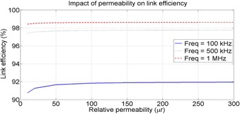
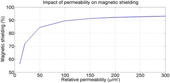
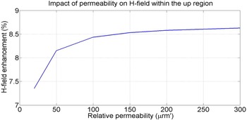
Figures 27–29 demonstrate that the analyzed descriptors (link efficiency, magnetic shielding, and H-Field enhancement) are improved when the relative permeability increases. There is a limitation effect, starting with a relative permeability of 100 where the link efficiency does not rise anymore. The magnetic field saturates the ferrite and performances will not significantly change for μ r ≥ 100 (the magnetic loss tangent, linked to the magnetic permeability, is not reported because its influence on WPT performances will be extremely low for classical permeability values).
Link efficiency as function of the magnetic permeability of the ferrite (other parameters frozen to their standard value).

Magnetic shielding as function of the magnetic permeability of the ferrite (other parameters frozen to their standard value).

H-field enhancement as function of the magnetic permeability of ferrite (other parameters frozen to their standard value).

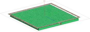
Maximum link efficiencies of 92% at 100 kHz and of 98.8% at 1 MHz were obtained by adding a ferrite with optimum parameters (illustrated in Fig. 30): (i) distance to the coil of 1.6 mm (thickness of the dielectric which supports the PCB traces in a real case); (ii) an area (250 mm2) lightly higher than the surface of the Tx coil; and (iii) a magnetic relative permeability μ′ rm = 100.
Model of the previous proposed Tx PCB coil with optimized ferrite.

Several conclusions and design recommendations emanate from this parametric analysis:
-
(i) the ferrite should be positioned as close as possible below the Tx coil and its area should be in the range of the PCB coil area (for link efficiency considerations but also on a magnetic field point of view);
-
(ii) a ferrite material with a relative permeability μ′ rm > 100 should be used. A higher permeability does not significantly improve the performances of the WPT system;
-
(iii) a ferrite properly positioned behind PCB coil can improve the generated magnetic field in the “up region” with at least 8% and attenuate the radiated magnetic field in the “down region” with at least 90%. So by a careful combination of all its parameters, the ferrite can be a valued asset for an optimized Tx power coil.
V. CONCLUSION
Coils are essential in inductive WPT systems and the use of PCB technology offers many freedom degrees in the design combined with a low-cost manufacturing process. Moreover this technology virtually offers an infinite diversity of shapes and sizes as well as easy integrations with other electronic devices and circuits. We proposed a modeling and simulation methodology for inductive WPT systems based on intensive full-wave simulation techniques in order to take into account not only the coil itself but also other elements (e.g. ferrite). The proposed simulation/modeling approach was validated through measurements on a reference PCB coil. A good trade-off between accurate modeling, computing resources, and time of simulation was found. A “coarse” mesh of 863 triangles and 2405 tetrahedra allows a simulation time of a few minutes with a reasonable cost of parallel computing (8 cores) Moreover, because the proposed approach is based on full wave simulations, it can be further extended on more complex WPT systems (by taking into account additional elements – Near Field Communication (NFC) coils, Global System Mobile (GSM) relay, etc. – integrated in the same WPT platform or the surrounding environment when the platform is integrated in more complex structures – furniture, cars, trains, etc.).
A parametric analysis based on full-wave simulations, and following the proposed modeling approach, was then performed in order to underline the influence of geometric parameters of the PCB coil on WPT performances.
The same approach is applied when a ferrite was positioned below the PCB coils, in order to quantify the influence of the geometric and magnetic parameters of the ferrite on WPT performances.
From the different parametric studies, an optimum PCB coil (15 turns, outer diameter: 44 mm, inner diameter: 10 mm, copper thickness: 70 µm, trace width: 1 mm, gap between traces: 0.1 mm) was derived. This PCB coil exhibits good performances at three different frequencies (100, 500 kHz, 1 MHz). Two descriptors named magnetic shielding and H-Field enhancement were introduced for quantifying the impact of a piece of ferrite positioned below the coil. For the selected PCB coil, the link efficiency, the magnetic shielding, and the H-field, enhancement increase if a ferrite properly selected is used.
Based on the conducted parametric analysis useful design guidelines for the ferrite selection were derived. An increase of the link efficiency, magnetic shielding, and H-field enhancement were observed when the ferrite is positioned very close to the coil and when its area is equivalent to the coil's one. There is no significant improvement for the magnetic shielding and the H-Field enhancement for ferrite with a relative magnetic permeability (μ′ rm ) greater than 100.
With optimum parameters, it is possible to reach link efficiency (without any piece of ferrite) from 88.7% (100 kHz) to 98.5% (1 MHz). After the adjunction of a piece of ferrite optimally dimensioned and positioned below the Tx coil, the link efficiency increases to 92% at 100 kHz and 98.8% at 1 MHz.
ACKNOWLEDGEMENTS
The authors acknowledge the financial support of Continental Automotive France [22] and of the French national association A.N.R.T (Association Nationale de la Recherche et de la Technologie) [23].
STATEMENT OF INTEREST
None.
 Guillaume Vigneau received a Master degree in electronics and radiocommunications from the french UPS University (Université Paul Sabatier) in 2012 and is currently doing his Ph.D. studies in wireless power transfer. His main research interests are on the improvement of wireless power transfer for low power devices, antenna and circuit design, applied in automotive environments.
 Mohamed Cheikh received a Master degree in electronics from ENSEEIHT engineering school in 2007 and received his Ph.D. degree in wireless communication in 2010. He now works on wireless car access and radiofrequency subjects in automotive environments.
 Rachid Benbouhout has Master degree in electronic engineering. After working on radiofrequency subjects as wireless car access, he is now the manager of the radiofrequency department at Continental Automotive France.
 Alexandru Takacs received his engineer diploma in Electronic Engineering from Military Technical Academy, Bucharest, Romania in 1999, Master (2000) and Ph. D. degree (2004) in Microwave and Optical Communications from National Polytechnic Institute of Toulouse, France. From 2004 to 2007 Dr. Takacs was Lecturer at Military Technical Academy of Bucharest and Associate Researcher at Microtechnology Institute of Bucharest. During 2011 he works as R&D RF engineer at Continental Automotive SAS France charged with antenna design and automotive electromagnetic simulation. Since 2012, Dr. Takacs is Associate Professor at University (Paul Sabatier) of Toulouse performing his Research within CNRS, LAAS Toulouse. His research interests include: design of microwave and RF circuits, energy harvesting and wireless power transfer, MEMS circuits and systems, small antenna design and optimization methods. He has authored or co-authored one book, 1 book chapter, and 15 papers in peer-review journals and over 70 communications in International Symposium Proceedings.