Introduction
The rapid advancement in recent wireless applications demands standard antennas to integrate multiple capabilities and functionalities such as the agile resonant frequency spectrum, polarization, and radiation pattern diversity on the same device. Reconfigurable antennas capable of frequency agility, pattern, or polarization provide an efficient solution to such requirements [Reference Christoudolou, Tawk, Lane and Erwin1]. Radiation pattern reconfigurable antennas are most demanded in secured communications to avoid the leakage of signal information. In electronic switching mechanisms, pin-diodes, RF-MEMS, or varactor diodes are commonly used switches [Reference Christoudolou, Tawk, Lane and Erwin1]. Moreover, electronically reconfigurable antennas fixed on the corridors, and vast halls reduce diminishing fields due to scattering by walls and other obstructions. In recent years, a lot of frequency and pattern reconfigurable antennas have been devised and reported. Antennas that provide frequency and pattern reconfigurability are proposed for various applications [Reference Li, Shao, Wang and Cheng2–Reference Zhang, Yan and Vandenbosch4]. A lot of radiation pattern reconfigurable antennas are proposed [Reference Lim, Yun and Lim5–Reference Lu and Yang12], such as omnidirectional to directional [Reference Lim, Yun and Lim5, Reference Lim and Lim8–Reference Zhang, Hong, Song and Wang10], directional beams in the opposite direction, broadside and end-fire direction [Reference Ding and Wang11], and multi-directional beams [Reference Jusoh, Aboufoul, Sabapathy, Alomainy and Kamarudin6] for various applications. A pattern reconfigurable antenna with eight switchable patterns of 45° steps in the azimuth plane and 36° vertical tilt angle for WiMAX and WLAN applications was reported [Reference Alam and Abbosh7]. In [Reference Li, Shao, Wang and Cheng2], the presented antenna is reconfigured to operate in monopole mode, patch mode to provide omnidirectional and direction patterns at 2.4 and 5.4 GHz, respectively.
Furthermore, in [Reference Zhu, Guo and Wu13], a dual-band antenna consisting of a circular monopole patch at 2.4 GHz and a U-slot square patch at 5.8 GHz is designed with a standard probe to achieve both omnidirectional and directional radiation patterns, respectively, in a single antenna. A small rectangular patch electrically connected to the ground plane of the rectangular monopole antenna is reported [Reference Liu, Qiu, Lan and Li14, Reference Kelly and Hall15]. Two monopoles sharing a common ground plane are proposed in [Reference Rahardjo, Zulkifli and Widiastri16], where one antenna is used for sensing and others for communication. A reconfigurable antenna utilizing the property of negative permeability of split-ring resonators is proposed for band-notched ultra-wideband (UWB) and narrowband applications [Reference Kandasamy and Ray17]. An optically controlled reconfigurable antenna is proposed in [Reference Jin and Zang18]. A mechanically reconfigured antenna is proposed in [Reference Tawk, Constantine, Avery and Christodoulou19]. A monopole antenna is presented that uses switchable slots in the ground plane to achieve reconfigurability [Reference Boudaghi, Azarmanesh and Mehranpour20]. A dielectric resonator antenna uses a PIN diode for switching and a varactor diode for fine-tuning the reconfigurable frequency bands [Reference Nejatijahromi, Naghshvarianjahromi and Rahman21]. The variation in high-frequency planar inductance and capacitance in patch antennas based on its shape and construction is presented [Reference Shlykevich, Bystricky and Blecha22]. A flexible, reconfigurable, and multiband antenna for wearable sensor applications was introduced [Reference Ghaffar, Li, Awan, Naqvi, Hussain, Alibakhshikenari and Limiti23–Reference Awan, Hussain, Naqvi, Iqbal, Striker, Mitra and Braaten25].
Moreover, to cover the 5G band, a radiation pattern reconfigurable antenna is presented in a study [Reference Zahra, Awan, Ali, Hussain, Abbas and Mukhopadhyay26] for IoT applications. The research articles mentioned above have failed to address a combination of single high-speed active antenna that can switch between directional radiation patterns (Ф ± 90°) resonates at low frequency (C-band) to omnidirectional antenna resonates at high frequency (X-band). Therefore, this paper introduces a design and development of a compact electronically switchable dual-band omnidirectional to the directional antenna for different applications of wireless sensor network (WSN) communication. The signal reception and transmission are performed by a single antenna inbuilt with the wireless network. The WSN has also been widely used in the industry, agriculture, military, transportation, and other fields.
An antenna to switch between omnidirectional to directional radiation patterns with frequency agility between X-band and C-band is presented in the proposed paper. In addition to this, a parametric simulation study is carried out by grooving staircase and semi-circular on the metallic portion of the radiator and reflector of the antenna system. Section “Antenna geometry and design methodology” gives the antenna geometry and design with detailed evolution steps of the printed rectangular monopole antenna (PRMA). Section “Working principle of proposed antenna” presents the simulation setup using the ANSYS HFSS EM simulator and the working principle of the proposed antenna. Section “Simulation analysis of antenna design” presents the parametric analysis of the dimension and position of the staircase and semi-circular grooving on the radiator and reflector. The Section “Fabrication and measurement” demonstrates the fabrication and measurement of antennas. In Section “Result and discussion,” there is an analysis of the experimental results.
Antenna geometry and design methodology
Antenna geometry of omnidirectional to directional and frequency-agile PRMA is designed and presented. The substrate material used is FR4 epoxy (εr = 4.4, loss tangent, δ = 0.025). The height of the substrate is chosen as 1.6 mm, with the thickness of the copper coating being 35 μm. The overall size of the antenna is 13 mm × 14 mm. The antenna system is responsive in the UWB frequency spectrum on complete removal of the ground plane. As shown in Fig. 1, initially, a rectangular substrate of size 13 × 14 mm2 (0.26 λ 0 × 0.28 λ 0) is selected where (λ 0 is the wavelength at the lowest edge of operating band). Two ground planes with a size of 3.7 mm × 4.5 mm are placed on both sides of the co-planar waveguide (CPW) feed with a width of 3 m, which is shown in Fig. 1(a). In the next step on evolution, the patch is symmetrically divided into radiator and reflector, as shown in Fig. 1(b). Figure 1(c) shows that the semi-circle slot on the radiator and reflector is used to fine-tune the resonant frequency in state-III. At the final stage of evolution, staircase slots were added to fragment the main patch (radiator and reflector), as shown in Figs 1(d) and 1(e). A novel proposed antenna with staircase and semi-circular-grooved slots is shown in Fig. 2, and is validated using HFSS.
Evolution stages of the antenna design: (a) step 1, (b) step 2, (c) step 3, (d) step 4, and (e) step 5.

Geometry of the proposed antenna. Note: L = 13 mm, W = 9 mm, Ws = 14 mm, S 1 = 2 mm, SW = 1 mm, R = 3 mm, and L3 = L4 = 4 nH, C1 = C2 = 0.5 pF, WG = 3.7 mm, GW = 1.3 mm, G = 0.5 mm, LG = 4.5 mm, FW = 3 mm, p = 4 mm; SW1, SW2 = SMP1340-04LF.

PRMAs are practically realized with finite-sized ground planes. The staircase-grooved rectangular monopole antenna is extended with the 50 Ω transmission line; it is matched with a load impedance of a simple rectangular monopole antenna [Reference Bhattacharjee27]. The printed monopole divides into symmetrical parts with thin slots and semi-circle grooving to achieve frequency reconfigurability and omnidirectional to directional (with pattern reconfigurability) radiation pattern. This balanced division makes the printed monopole act as a radiator and reflector. The width of feed, dielectric constant (ɛr), and thickness (h) of the substrate are chosen based on the standard microstrip transmission line for properly matching the printed monopole with the microstrip feed line. Thus, a CPW microstrip-fed PRMA can be considered an asymmetrically driven dipole antenna. It can be further realized as a combination of radiator and reflector and staircase grooving on the radiating element. In printed monopole antennas, the radiation field is found by considering the contribution of both the patch and the ground plane. The standard formulation of resonance frequency after modification [Reference Ray28] to design a rectangular monopole is given in equation (1):

where p is the length of the 50 Ω feed line, L is the length of the rectangular planar monopole antenna, and q is the effective radius of the equivalent cylindrical monopole antenna, which is determined by equating the area of the planar and cylindrical monopole antennas. For PRMAs, L and q are calculated [Reference Bhattacharjee27, Reference Ray28] as follows in equation (2):

where L is the length and W is the width of the PRMA.
PRMA is a variation of microstrip antenna, in which the ground plane is located at the same plane. Following this analogy, the factor k in equation (1) has similar significance as √ɛeff. With commonly used FR4 substrate of ɛr = 4.4 and h = 1.6 m, the practical value of k = 1.15 estimates the resonance to be within 10%. Equation (1), with k = 1.15, has been validated for the proposed staircase and semi-circular-grooved PRMA configurations.
The staircase grooving increases the length of surface current helps in achieving the response at the C-band frequency spectrum in states-I and -II. The increased electric length improves the impedance matching of the CPW feed (50 Ω) and free space impedance (377 Ω). Switching between the C-band and X-band can be implemented through the symmetrical division of the radiating patch. Impedance matching is obtained without using any matching stub. The antenna consists of a rectangular patch, symmetrically separated by a staircase groove and semi-circular slots.
The SMD PIN diodes and lumped elements are adequately placed, as shown in Fig. 2. A CPW feeding the two symmetrically slot-loaded patches offers directional radiation patterns (states-I and -II) with a Ф = 180° phase shift at 6.185 and 5.715 GHz, respectively, and an omnidirectional radiation pattern (state-III) is obtained at 9.95 GHz. States-I and -II offer a bandwidth of 1660 and 1750 MHz, respectively, and state-III provides a bandwidth of 1860 MHz.
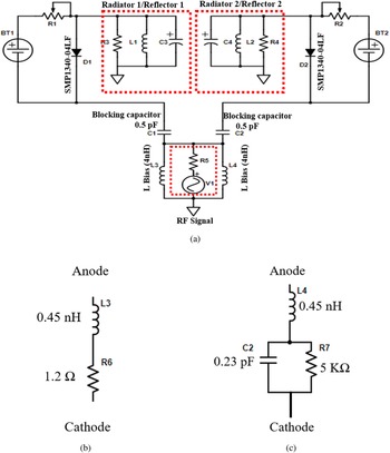
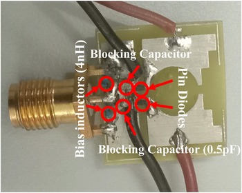
The SMD PIN diodes, SMP1340-04LF (Skyworks), are used for switching in this proposed antenna system. The characteristics of the SMD PIN diode, total capacitance circuit of the SMD PIN diode, and switching circuit are shown in Fig. 3. Two bias inductors (LBias = 4 nH) are placed between the RF feed and grounds to block unwanted RF currents. It will also compensate the current phase shift by leading the exciting current equivalent to lag in exciting current due to total capacitance of SMD PIN in the OFF state. Capacitors (CB = 0.5 pF) are placed between the antenna and SubMiniature version A (SMA) connector to block DC voltage toward the RF input signal. In the ANSYS HFSS simulator, blocking capacitors (CB = 0.5 pF), bias inductor (LBias = 4 nH), and SMD PIN diode are modeled using lumped elements during the simulation, and it is vulnerable to fabrication imperfections.
(a) Diode bias switching circuit of antenna. (b) Equivalent circuit of PIN diodes at ON conditions. (c) Equivalent circuit of PIN diodes at OFF conditions.

Working principle of proposed antenna
ANSYS HFSS EM simulator is employed to simulate the proposed PRMA with different switching configurations of SMD PIN diodes. Two PIN diodes are used for switching between C-band and X-Band frequency spectra. Both the diodes are in the OFF state, the radiator and reflector are electrically isolated from the excitation of the antenna system. Therefore, in this state, there is no response for antennas. With either state of the diode (i.e. ON and OFF), radiating metallic patch will act as radiator and reflector alternatively making the antenna system to configure to the directional radiation pattern with a 180° phase shift (i.e. Ф = 270° and Ф = 90°). The required radiation pattern, either directional or omnidirectional, can be accomplished from the same device through an electronic switching mechanism. The switching mechanism is implemented only with two SMD PIN diodes, as shown in Fig. 3. The PIN diode SMP1340-04LF from Skyworks is used, and its equivalent circuit model is considered for simulation. The equivalent electrical model of the diode is done by utilizing lumped elements. Therefore, for the ON state, the diode behaves like a series combination of 0.45 nH inductor with 1.2 Ω resistor, whereas for the OFF state, the diode behaves like a series combination of 0.45 nH inductor and a parallel combination of 5 kΩ resistor and 0.23 pF capacitor.
Two inductors L3 and L4, acting as biasing inductors, will compensate for the lag in RF exciting current due to total capacitance of diode in the OFF state of the diode. Two capacitors C1 and C2 are connected and act as DC blocking capacitors, providing better RF connectivity in the design. In state-I, the switch SW1 is ON and switch SW2 is OFF, the right-hand part of the patch acts as a radiator, and the left-hand portion acts as a reflector, and the fields are radiated in the Ф = 270° direction. In state-II, switch SW1 is OFF and switch SW2 is ON, the left-hand part of the patch radiates, and other reflects that cause the fields to radiate toward the Ф = 90° direction. In state-III, both switches (SW1 and SW2) are in the ON state, and both halves act as radiators. The fields are radiated in the omnidirectional pattern at Ф = 0° and Ф = 180°. Thus, the proposed antenna is designed to operate in three states to produce three different radiation patterns. Two patterns are directional, and the other is an omnidirectional radiation pattern. Figure 4 depicts the three states depending on the various combinations of the switches, and its status is shown in Table 1.
Operating states of the antenna: (a) state-I, (b) state-II, and (c) state-III.

Frequency response for status of states of switches

Simulation analysis of antenna design
The simulation analysis has been performed on three different states, as listed in Table 1. This section is devoted to study the variation of resonance frequency, reflection coefficient, and radiation pattern, and it is observed. The frequency response at each evolution step of an antenna for the states-I and -II are shown in Fig. 5. It is in the C-band. In state-III, it is in the X-band, and it is shown in Fig. 6.
Reflection coefficient (S 11) of PRMA in states-I and -II for all evolution steps.

Reflection coefficient (S 11) of PRMA in state-III for all evolution steps.

In the simulation analysis, a parametric study of physical parameters, the radius of semi-circular is performed. The parametric analysis allows tuning the resonance frequency since the gap between the radiator and reflector offers the magnetic capacitance effect. Based upon this analysis, three different cases are deduced, as given below:
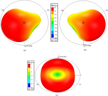
I. Case i: In this case, the switch is in state-I, where diode D1 is ON, and diode D2 is in OFF condition. Figure 7 shows the shift in the resonance frequency toward the lower frequency C-band since an increase in the radius provides a lengthier current path. The directional radiation pattern with a total gain of 2.1 dBi at Ф = 270° is observed at 6.07 GHz (4.94–6.6 GHz) for voltage standing wave ratio (VSWR) ≤2.0.
II. Case ii: The switch is in state-II, where diode D1 is OFF, and diode D2 is in ON condition. Figure 7 shows the shift in the resonance frequency toward the lower frequency band since an increase in the radius provides a lengthier current path. The directional radiation pattern with a total gain of 2.1 dBi at Ф = 90° is observed at 6.07 GHz (4.92–6.63 GHz) for VSWR ≤2.0.
III. Case iii: The switch is in state-III, where diode D1 is ON, and diode D2 is in ON condition. Figure 8 shows the shift in the resonance frequency toward the upper-frequency band and omnidirectional radiation pattern with a total gain of 4.1 dBi at Ф = 0° and Ф = 180° is observed at 9.95 GHz (8.82–10.68 GHz) for VSWR ≤2.0.
Reflection coefficient (S 11), parametric study in states-I and -II.

Reflection coefficient (S 11), parametric study in state-III.

The optimum value of radius of the circle is chosen as 3 mm. The parametric study of the proposed antenna for different semi-circular slot radii (R) for states-I, II, and III is given in Figs 7 and 8, and the results are tabulated in Table 2.
Frequency response of parametric study on various radii of semi-circle slot

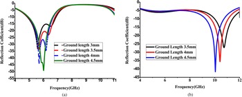
The spacing between the patch and ground and feed line and ground develop capacitance effect causes variation in the resonance frequency. So here, it is fixed as 1.3 and 0.5 mm, respectively, to achieve 6 and 10 GHz frequency. Changing the size of the antenna ground will affect the resonance frequency and the reflection coefficient, as shown in Fig. 9. The parameter study shows that 4.5 mm is a better antenna ground length to achieve both required resonance frequencies. The width of the feed line mainly affects the impedance here, and it is tuned for 50 Ω for both resonance frequencies. Here, it is fixed as 3 mm. The length of the feed line will cause the variation of PRMA resonance frequency. This relation is presented in Section “Antenna geometry and design methodology” of the paper, where the variable p is the length of the feed line.
Parametric study on ground length variation (LG) at: (a) state-I and state-II and (b) state-III.

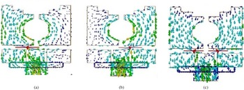
The current flow to the antenna is due to the RF excitation. The diode state will decide the current flow in the patch. State-I will excite the radiator on the right side, whereas state-II will excite the radiator on the left side. In state-III, both the symmetrical patches will act as radiators. In state-I, the maximum current distribution lies at the edges of the left patch and left ground that will work as the radiator and gives the resonance frequency at the C-band. In state-I, the right-side patch current distribution is minimum, but the current is more at the curved side of this patch, showing that this patch acts as a reflector. Therefore, the radiation pattern will reflect toward φ = 270°. In state-II, the action is just reversed with the support of the switching mechanism provided. Therefore, the direction of the radiation pattern will move toward φ = 90°. In state-III current distribution on both patches and grounds is equal so that both patches could act as radiators. In this state, the resonance frequency is shifted at the X-band, and it provides an omnidirectional radiation pattern. The frequency response and radiation pattern are acts of current flow in the radiating patch of the antenna system. The surface current distribution based on different states-I, -II, and -III is shown in Figs 10(a)–10(c), and its corresponding 3D radiation pattern is shown in Figs 11(a)–11(c).
(a) Surface current distribution, state-I. (b) Surface current distribution, state- II. (c) Surface current distribution, state-III.

3D Radiation pattern for (a) state-I, (b) state-II, and (c) state-III.

Figure 12 shows the total simulated gain with varying frequency of three different diode states (i.e. states-I, -II, and -III). It is proved that the maximum gain is 2.1 dBi at resonance frequency 6.185 GHz in state-I and 5.715 GHz in state-II. In state-III, the maximum gain of 4.1 dBi is observed at resonance frequency 9.93 GHz. The simulated radiation efficiency of the antenna in states-I, -II, and III is approximated to 86–87%. Figure 12 shows that the radiation efficiency is comparatively high throughout the C-band and X-band.
Simulated total gain versus frequency and efficiency versus frequency in states-I, -II, and -III.

Fabrication and measurement
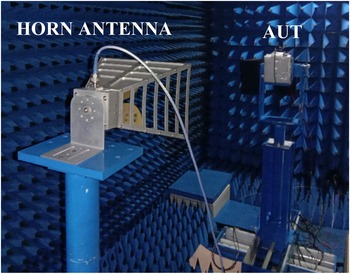
The PRMA is fabricated, and the antenna parameters are measured. The printed circuit board (PCB) etching method with RMI UV laser etching and cutting is used to print the metallic radiating patch, and then staircase and semi-circular slot are grooved from the metallic part of the radiating patch. The bottom layer is completely removed from the low-cost substrate material. An SMA connector is soldered to the microstrip transmission line of PRMA to excite an antenna with 50 Ω input impedance to match with load impedance for maximum power transfer. A proper biasing circuit to avoid coupling the RF signal and the DC bias current is shown in Fig. 13. Surface mount capacitors of 0.5 pF were used for blocking DC bias current. A proper series resistance maintains minimum bias current through the pin diodes. An inductor (4 nH) is used to compensate for the current lag by the total capacitance of the diode in states-I and -II. The biasing voltage of 1.5 V is provided by a series connection of regulated power supply. Figure 13 shows the fabricated PRMA with biasing and switching modules. Figure 14 shows the setup for measurement of reflection coefficient (S 11) and radiation pattern in an anechoic chamber. In this approach, a calibrated vector network analyzer (VNA) measures the reflection coefficient (S 11) and radiation pattern. The antenna system under test is excited by a flexible co-axial cable connected with VNA to the SMA connector of the PRMA.
Fabricated PRMA with biasing and switching module.

Anechoic chamber setup for measurement of AUT.

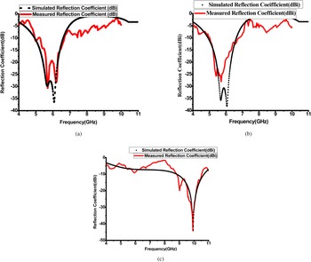
The measured 10 dB return loss bandwidth is compared with the simulated result in Fig. 15. A good agreement is observed since the measured and simulated results for the reflection coefficient are overlapped. The measured bandwidth for RL < −10 dB is 6.185 GHz (5.275–6.675 GHz) in state-I and 5.715 GHz (5.05–6.8 GHz) in state-II. In state-III, the measured bandwidth is 9.93 GHz (8.845–10.49 GHz). The simulated and measured frequency responses are plotted and shown in Fig. 15(a) for state-I, in Fig. 15(b) for state-II, and in Fig. 15(c) for state-III.
(a) Reflection coefficient (S 11) for state-I, (b) reflection coefficient (S 11) for state-II, and (c) reflection coefficient (S 11) for state-III.

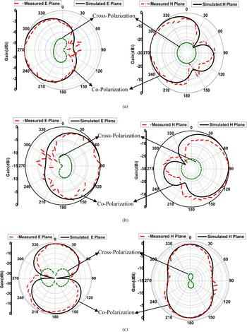
The absolute gain is measured by a known antenna gain measured method. In this approach, a calibrated VNA measures S 21 in between the pairs of antennas inside the anechoic chamber of SSN Research Centre, Anna University. A well-known horn distance (2 m) and setup unchanged measurement is performed for different azimuth and elevation plane by keeping the antenna in the vertical plane. In contrast, the antenna under test (AUT) rotates in 360° and measures radiation patterns in the E-plane (x–y plane) and H-plane (x–z plane). In the azimuth and elevation plane, the RMS value of gain is 2.1 dBi at 6.185 and 5.715 GHz with directional radiation pattern for states-I and -II and 4.1 dBi at 9.93 GHz with omnidirectional radiation pattern for state-III. The co-polarization and cross-polarization plot of E-plane and H-plane of the measured and simulated radiation patterns is mapped in Fig. 16. There is good agreement between the measured and simulated radiation patterns over both in C-band and X-band.
(a) Normalized measured and simulated E-plane (x–y plane) and H-plane (x–z plane) in state-I, (b) normalized measured and simulated E-plane (x–y) plane and H-plane(x–z) plane in state-II, and (c) normalized measured and simulated E-plane (y–z plane) and H-plane (x–z plane) in state-III.

Results and discussion
The design, simulation, and analysis of the antenna are performed using computer simulation technology. The fabricated prototype antenna is shown in Fig. 13. The alternate behavior of radiator and reflector of the two symmetrical half patches, for all the three states, can be identified from the surface current distributions and corresponding polar plot of radiation patterns of the proposed antenna, as illustrated in Figs 10 and 16. The antenna provides directional patterns at Ф = 270° and Ф = 90° directions with a directivity of 2.1 dBi for states-I and -II. To activate the different combinations of switches, biasing voltage is given by the DC voltage source. The supply voltage to make PIN diode ON is 1.5 V and maintained the forward PIN diode current minimum of 1.5 mA for the prescribed frequency. Agilent VNA is calibrated before measuring the reflection coefficient for each state. The simulated and measured reflection coefficient, the S 11 parameter, is shown in Fig. 15 for the three different states. For state-I simulation, the antenna resonates at 6.07 GHz (4.94–6.6 GHz), and for state-II, the antenna resonates at 6.07 GHz (4.92–6.63 GHz) in the C-band; while for state-III, the antenna resonates at 9.95 GHz (8.82–10.68 GHz) in the X-band. The proposed antenna resonates from 5.275 to 6.675 GHz in state-I and 5.05 to 6.8 GHz in state-II in the measured results; whereas in state-III, it resonates from 8.845 to 10.49 GHz. There is a slight variation in resonant frequency, reflection coefficient, and in its bandwidth. These discrepancies are mainly due to the insertion of biasing circuitry with its wires, discrete components, small ground plane size, and comparable SMA connector size. Prototype antennas also introduce a smaller unexpected mismatching between simulated and measured reflection coefficient due to the fabrication imperfection and the mutual coupling between reflector and ground patches.
The simulated and measured gain results are in good agreement with each other at the reported frequencies. However, in this compact planar monopole antenna, the reflection characteristics of all the states are well below −10 dB, indicating a good impedance matching at the resonant frequency bands. The antenna provides a total gain in the range of 2.1 dBi for the directional pattern and 4.1 dBi for the omnidirectional pattern. The radiation efficiency of 86–87% is achieved for the three states due to the losses introduced by antennas with biasing circuits. The measured beamwidth of states-I and -II in the E-plane is higher than that in the state-III and provides broader coverage.
Figure 16 illustrates the antenna's measured and simulated radiation patterns. It is realized that in states-I and -II, the radiating fields are directional, that is, Ф = 270° and Ф = 90°, respectively, in the H-plane. In contrast, in state-III, the radiating fields are in the omnidirectional pattern in the E-plane. Table 3 shows the comparison of proposed antennas with previous studies.
Comparison of proposed antenna with references

The significant contribution of the proposed study compared with prior research can be summarized as follows:
(i) The via-free design offers a simple and compactable structured antenna with a reduction of inductance variation, which can cause resonance frequency variation and pattern reconfigurability.
(ii) The antenna utilizes only two PIN diodes to switch between two frequencies bands (6 and 10 GHz) and pattern reconfigurability at 6 GHz (5G-sub-6-GHz).
(iii) The antenna offers good performance and mechanical robustness, which can be implemented on the same PCB as other electronic devices needed for upcoming WSN communication systems.
(iv) Comparison with state of the artwork states that the presented antenna over-performs the related studies by providing an overall better performance and a good agreement between simulated and measured results, as depicted in Table 3.
Conclusion
A compact and electronically switchable omnidirectional to directional radiation pattern frequency-agile PRMA is designed, simulated, and measured. The antenna is capable of frequency reconfiguration by using PIN diodes between C-band and X-band with radiation patterns from directional either at Ф = 90° or Ф = 270° to the omnidirectional pattern at Ф = 0° and Ф = 180°, respectively. It had been achieved by selectively CPW feeding and grounding the portion of the antenna system in the same layer. The antenna provides a realized gain of 2.1 dBi and radiation efficiency of around 86–87%. Thus, the proposed antenna offers a novel, less complex, and efficient omnidirectional to directional radiation pattern and frequency agility solution for C-band (5275–6.675 GHz and 5.05–6.8 GHz) and X-band (8.845–10.49 GHz). The proposed antenna is most suitable for wireless networks deployed to monitor different states of chemical reactors in industries such as oil and gas, pharmaceuticals, chemicals, etc.
Acknowledgements
This study is supported by the RF and Microwave laboratory of the SSN Research Center (SSNRC) for the design and analysis of the antenna. The Department of Science and Technology, India, funded an anechoic chamber at SSN College of Engineering (SSNCE), Anna University, India, to measure and test an antenna system.
 Melvin Chamakalayil Jose received his B.E. degree in Electronics and Communication Engineering from Bharathidasan University in 2002, and his Master of Engineering in Power Electronics from Amrita University, Coimbatore, India in 2008. He has 12 years of teaching experience in reputed institutions in Kerala. He is currently working toward his Ph.D. degree at Anna University, Chennai. He is a research scholar in the Department of Electronics and Communication Engineering, SSN College of Engineering, Chennai. His primary research interests are broadband array antennas, reconfigurable antennas, and FSS structures for wireless communication applications.
 Radha Sankararajan is the Professor & Head of Department of ECE, and has 26 years of teaching and 13 years of research experience in the area of mobile ad hoc networks. She has graduated from Madurai Kamaraj University, in Electronics and Communication Engineering in 1989. She has obtained her Master's degree in Applied Electronics with First Rank from the Government College of Technology, Coimbatore and her Ph.D. degree from the College of Engineering, Guindy, Anna University, Chennai. She also worked as a visiting researcher at Carnegie Mellon University, USA for a period of 6 months in the area of wireless sensor networks. She has 72 publications in international and national journals and conferences in the area of mobile ad hoc networks and wireless sensor networks. She has received IETE – S. K. Mitra Memorial Award in October 2006 from the IETE Council of India, Best paper awards in various conferences, and CTS – SSN Best Faculty Award – 2007 and 2009 for the outstanding performance for the academic years 2006–2007 and 2008–2009.
 Balakrishnapillai Suseela Sreeja received her B.E. from Bharathidasan University in 2002, and her M.E. and Ph.D. degrees from Sathyabhama University in 2004 and 2012, respectively. She has 14 years of teaching experience in various universities, including Sathyabhama University, India, Linton University College, Malaysia, and SSN College of Engineering, India. Her research interests include high-frequency devices and structures, smart devices, MEMS and NEMS devices, and co-integration of devices and circuits.
 Mohammed Gulam Nabi Alsath received his BE, ME, and Ph.D. degrees from Anna University, Chennai in 2009, 2012, and 2015, respectively. He is currently serving as an Associate Professor in the Department of Electronics and Communication Engineering, SSN College of Engineering, Chennai, India. His research interests include microwave components and circuits, antenna engineering, signal integrity analysis, and solutions to EMI problems. To his credit, he has filed 12 patents and published several research articles on antennas and microwave components in leading international journals. He has also presented and published his research papers in the proceedings of international and national conferences. He is currently serving as an Associate Editor in IET Microwaves Antennas and Propagation.
 Pratap Kumar received his B.Tech. degree in Electronics and Communication Engineering from Bharath University in 2007, and his Master of Engineering in Communication Engineering from Anna University, Coimbatore, India in 2017. He is currently working toward his Ph.D. degree at Anna University, Chennai. He is a research scholar in the Department of Electronics and Communication Engineering, SSN College of Engineering, Chennai. His primary research interests are re-configurable antennas and RF and microwave engineering for wireless communication applications.