Introduction
The efficient and clean conversion of heat into electric power is a crucial challenge today. Recognizing that thermionic energy conversion Reference Hatsopoulos and Gyftopoulos1 may achieve high efficiencies, numerous analyses have suggested that the thermionic conversion process can meet this challenge. Reference Moyzhes and Geballe2,Reference Meir, Stephanos, Geballe and Mannhart3 The so-called space-charge problem—electrons between the cathodes will generate a potential barrier—reduces the effectiveness of standard thermionic energy conversion to unacceptably small values. Reference Hatsopoulos and Gyftopoulos1 However, thermoelectronic energy conversion Reference Meir, Stephanos, Geballe and Mannhart3 solves the space-charge problem by removing the space charge with electric-gate fields.
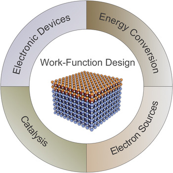
In this article, we present this conversion process, summarize the studies conducted to analyze its potential, and critically assess its possibilities and challenges. The success of thermoelectronic energy conversion hinges on developing materials with designed and small work functions as well as high electron emissivity that are stable under high-temperature operating conditions. Materials with engineered work functions are of prime interest for thermionic and thermoelectronic energy conversion as well as for numerous other applications such as electron sources, Reference Wanke, Hassink, Stephanos, Rastegar, Braun and Mannhart4 electronic devices, Reference Reisch5 and catalysis Reference Vayenas, Bebelis and Ladas6 ( Figure 1 ).
Engineering work functions are key to enabling numerous and diverse applications of complex materials.

Principle of thermoelectronic energy conversion
A conducting electrode heated to high temperatures emits electrons. Reference Becquerel7–Reference Edison9 These electrons overcome the electrode’s work function and generate a thermionic emission current. Simon and Schlichter Reference Schlichter10 were the first to recognize that thermionic electron emission could be an efficient way to convert energy, if a second, colder electrode, a collector, is placed next to the emitter. The emitted electrons condense on the collector and generate an imbalance of the electrochemical potential of both electrodes. The maximum output voltage of such a device is determined by the difference in the work functions of the two electrode materials. Such a system essentially requires only the two contacted electrodes mounted in vacuum. It is therefore feasible to operate the two electrodes with an exceptionally large temperature difference, yielding high Carnot efficiencies. Because thermoelectronic energy converters obviously are thermal machines, the Carnot efficiency represents the ultimate efficiency limit.
However, the thermionic energy-conversion process faces severe challenges, the most important is known as the space-charge problem—the electrons traveling in vacuum generate a negative electrostatic potential that suppresses the emitter-collector current. One possible solution to this problem is to neutralize this space charge by injecting positive ions (such as Cs+) into the electron cloud. Reference Novikov11 The TOPAZ power generators in two Soviet satellites delivered up to 5 kW using this technique. However, generating and injecting the Cs+ ions limits the efficiency to 5.2%. Reference Gryaznov12
A second approach to solving the space-charge problem is to reduce the absolute number of electrons in the interelectrode space by narrowing the electrode spacing to a few micrometers. Reference Belbachir, An and Ono13–Reference Lee, Bargatin, Melosh and Howe16 This reduces the space charge enough to allow current densities on the order of 1 A/cm2. In a third approach, additional positively charged electrodes are used to draw the space charge away from the emitter. Investigations of this concept were apparently stopped in 1973, when, based on a series of experimental studies, it was deemed to be impractical. Reference Hatsopoulos and Gyftopoulos1
In an alteration of the latter approach initiated in 2009, Reference Meir, Stephanos, Geballe and Mannhart3 electrostatic and magnetic fields were applied to the interelectrode space ( Figure 2a). To generate the electrostatic field, an electrode known as a “gate” is inserted between the emitter and the collector. This gate is positively biased at several volts with respect to the emitter to accelerate the electrons from the emitter, as shown in the band diagram in Figure 2b. Upon passing through the gate, the electrons return this kinetic energy to the gate field. Care must be taken to minimize currents that are lost to the gate because, owing to the high gate voltage, losses are large even for small gate currents. To reduce gate currents, a magnetic field is applied parallel to the averaged electron trajectories. Whenever an electron acquires a velocity component transverse to the magnetic field, for example, due to the attracting electric field of a gate wire, it gyrates around the magnetic field line. This effect prevents the electrons from being drawn into a gate wire. Reference Meir, Stephanos, Geballe and Mannhart3
(a) Sketch of a thermoelectronic energy converter. Input energy (heat, Q
in, or photons, hνin) absorbed in the top electrode (emitter) causes the emission of electrons. The resulting emitter-collector current and the generated difference in the electrochemical potential between emitter and collector give rise to the electric output power (
 $P_{{\rm{out}}}^{{\rm{el}}}$
). If an electron-transparent material is used for the gate, no magnetic fields are required. (b) Band diagram of a thermoelectronic energy converter under optimal load conditions. The electrons that overcome the work function of the emitter (left) are transferred to the collector (right). The gate (middle) shapes the Coulomb potential to yield a high emitter-collector current. Note: h, Planck’s constant; νin, photon frequency; V
G gate bias; B, magnetic field; E
VAC, vacuum energy; ϕem, emitter work function; ϕcoll, collector work function; μem, emitter chemical potential; μcoll, collector chemical potential; V
load, load voltage; f
em, Fermi–Dirac distribution of the electrons in the emitter; f
coll, Fermi–Dirac distribution of the electrons in the collector; E, energy.

Another way to reduce electron absorption in the gate is to fabricate the gate from perforated two-dimensional (2D) materials with a small absorption coefficient such as perforated graphene. Reference Hassink, Wanke, Rastegar, Braun, Stephanos, Herlinger, Smet and Mannhart17 In the energy range of 1–20 eV, which is the relevant energy range in the conversion process, the absorption coefficient for electrons in nonperforated graphene equals 30–40%. If gate materials with vanishing electron absorption are used, magnetic fields are not needed. As such, converters essentially consist of only the contacted emitter, gate, and collector electrodes—possibly in the form of foils or even 2D materials. Their masses can be extremely small, making them attractive for mobile applications. Reference Wanke, Hassink, Stephanos, Rastegar, Braun and Mannhart4
The fundamental idea behind thermoelectronic energy conversion is to use electromagnetic fields to convert an energy input into an electrochemical potential difference. The underlying principle can be applied to thermionic emission, emission by the photoelectric effect, photon-enhanced thermal emission, Reference Schwede, Bargatin, Riley, Hardin, Rosenthal, Sun, Schmitt, Pianetta, Howe, Shen and Melosh18 and tunneling emission. Being independent of thermionic emission, this energy-conversion process in which space charges are suppressed by gate fields is called thermoelectronic energy conversion. Reference Meir, Stephanos, Geballe and Mannhart3 It is basically related to thermoelectric conversion, the thermoelectrically active material being replaced by vacuum. Vacuum is characterized by a large Seebeck coefficient, which quantifies the ability of a material to generate a thermoelectric voltage from a temperature difference. This is determined by the entropy of the electrons, by a relatively small thermal conductivity due to the absence of phonons, and by a large electrical conductivity due to the ballistic nature of electron transport.
The work functions of the emitter and collector are one of the main factors that determine the efficiency of the conversion process. Previous technologies such as radio-tube electronics or cathode-ray tube displays depended on efficient electron-emitting materials. The search for the best performing materials goes back more than a century with the discovery of electron emission from refractory metals, notably, tungsten. Reference Edison9 Unfortunately, many of these metals are not stable at the temperatures required to emit sufficient currents and also have large work functions. The resulting high temperatures lead to serious technological challenges.
This was mitigated in the 1900s and 1910s, when alkaline-earth-metal oxide coatings with much smaller work functions were discovered. Reference Tyne19,Reference Blewett20 Typical oxides investigated included BaO, SrO, CaO, and their solid solutions. These coatings reduce the work function by providing electric dipoles on the metal surface. A layer of BaO applied to tungsten, for example, reduces its work function from 4.5 eV to 2.1 eV and thereby lowers the operating temperature substantially. As these oxides are unstable in air, they are deposited as carbonates, which are then activated at high temperatures.
Large-scale efforts were invested during the development of so-called dispenser type cathodes, resulting in significant increases of current density and lifetime. In these cathode materials, oxides are embedded into the voids of porous tungsten matrices to replenish oxide molecules that evaporate from the cathode surface. Additional coatings such as osmium/ruthenium layers can reduce the work function by 0.1–0.5eV. Reference Cronin21 Typical thermionic current densities of such dispenser cathodes are on the order of 10 A/cm2 (1000°C). Reference Cronin21 These cathode materials are used in many applications today.
In the 1950s, another material system, borides, such as LaB6 and CeB6, which have work functions of ∼2.6 eV, were discovered as electron emitters. Reference Lafferty22 These materials feature high evaporation temperatures, rather small work functions, robustness toward contamination, and thermionic emission currents in the range of 20 A/cm2 (1400°C). At the same time, in the TOPAZ program, cesium oxide-coated cathodes were developed. Reference Novikov11 Cesium oxide reduces the work function below 2 eV, with reported values as small as 1.2 eV. Reference Shiota and Miyamoto23 These discoveries caused a 50-year slowdown in the search for materials with optimized work functions, because the then existing technology solved most application problems at low cost. In recent years, dispenser-type cathodes have been further improved Reference Giordano, Cinquini and Pacchioni24–Reference Vaughn, Wan, Jamison and Kordesch26 for larger current densities and lower work functions. For example, Sc2O3-doped tungsten impregnated with BaO:CaO:Al2O3 shows current densities of up to 100 A/cm2 (800°C), Reference Wang, Wang, Liu, Zhang and Li27 and work functions <1 eV were demonstrated for Ca24Al28O64. Reference Toda, Matsuishi, Hayashi, Ueda, Kamiya, Hirano and Hosono28
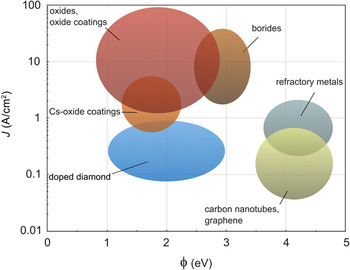
New materials and technologies for material synthesis have widened this field in the last decade. For example, doped diamond synthesized by precisely controlled chemical vapor deposition methods provides a new class of promising electron-emitter materials. Doped diamond is stable at high temperatures and, when doped with, for example, nitrogen, has a work function of only 1.7 eV. Reference Koeck and Nemanich29,Reference May, Stone, Ashfold, Hallam, Wang and Fox30 Remarkably, P-doped diamond can show work functions of approximately 1 eV while still maintaining its thermal and mechanical properties. Reference Koeck, Nemanich, Lazea and Haenen31,Reference Koeck, Nemanich, Balasubramaniam, Haenen and Sharp32 Promising electron emission is also shown by carbon nanotube (CNT) forests. Reference Khoshaman, Fan, Koch, Sawatzky and Nojeh33 While CNTs have work functions >4 eV, the thermal conductivity of the one-dimensional nanotubes is so low that a temperature gradient of 1000 K/mm is easily achieved. Reference Khoshaman, Fan, Koch, Sawatzky and Nojeh33 Closely related to CNTs are graphene sheets, which have been reported to show encouraging electron-emission characteristics. The work function of graphene can be tuned by either chemical or electrostatic doping. Reference Zhao, Ryu, Brus, Kim and Kim34,Reference Chang, Lin, Taur, Chen, Liao, Pi, Chen and Wu35 However, in these novel low-work function material classes, high emission current densities have yet to be demonstrated. Figure 3 summarizes the work functions and current densities of state-of-the-art materials.
Overview of work functions (ϕ) and reported emission current densities (J) for several families of materials used as electron emitters. Perovskites are not shown, because, to our knowledge, results of emission current density measurements have not yet been reported for this class of materials.

Zhong et al. Reference Zhong and Hansmann36 recently explored the possibility of tuning the work function using perovskite heterostructures. Many perovskites are stable at high temperatures and under oxidizing conditions. They can be grown with atomic precision by molecular beam epitaxy or pulsed layer deposition, benefiting from the tuning of interface and surface properties using band engineering. By controlling the atomic-scale stacking sequence, tunable charge transfer between layers and control of the work functions is achieved. As the perovskite oxide family is large and contains members with diverse electronic properties, the parameter space for such artificial materials is enormous.
Experimental studies
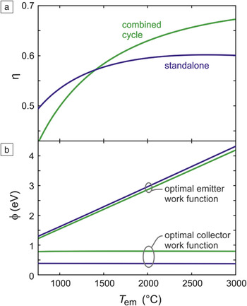
Numerical models of thermoelectronic energy conversion yield encouraging results Reference Meir, Stephanos, Geballe and Mannhart3 ( Figure 4 ). According to these models, efficiencies greater than 50% seem possible for standalone thermoelectronic energy converters and greater than 60% for a combined-cycle system (a thermoelectronic generator combined with a heat engine that is optimized for lower input temperatures, such as a steam turbine). To understand whether high-efficiency thermoelectronic energy conversion is realistic, the process needs to be examined because of the many engineering and materials science challenges involved. These challenges may well be overcome by gradual developments. We have focused our experimental investigations on searching for hidden fundamental problems and bottlenecks. We created several generations of converters. For reproducibility, these converters are operated in ultrahigh vacuum environments. Magnetic fields are generated by permanent magnets; silicon, tungsten, and graphene have been explored as gate materials. As emitter and collector materials, a variety of compounds, including La2O3:W, ZrO2:Mo, LaB6, and BaO:W have been investigated.
Calculated efficiency limit of a standalone converter (blue) and a combined system (green) as a function of emitter temperature. The curves in panel (a) refer to the direct conversion efficiency (η), whereas the ones in (b) show the work functions (ϕ) that yield the maximum efficiencies for a given emitter temperature (T em). For the standalone converter, the collector is kept at 50°C; for the combined cycle system, the collector is operated at 400°C, and the efficiency of the steam turbine is taken to equal 32%. These results show that thermoelectronic energy conversion yields very high efficiencies and can even enhance state-of-the-art energy-conversion technologies.

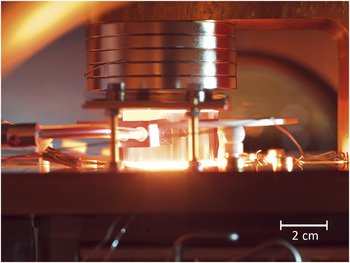
Figure 5 shows a photograph of a state-of-the-art converter in operation. In this system, the emitter is heated indirectly to 1700°C by a hot foil. In this setup, in situ piezoelectric actuators are deployed to vary the interelectrode gap, for studies of the influence of the gap width on device performance. In our experiment, the electrodes have a typical cross-sectional area of several square centimeters. These studies demonstrate the effectiveness of combining a grid and a magnetic field, Reference Meir, Stephanos, Geballe and Mannhart3 thereby confirming the principle of thermoelectronic energy conversion. Our studies also show that unsuitable field configurations caused the issues that led to gate fields being rejected as a solution of the space-charge problem in the 1970s. For example, two parallel plates alongside each other, where the electrons are guided by a magnetic field, still showed regions with strong space charge. Reference Hatsopoulos and Gyftopoulos1
Photograph of a thermoelectronic energy converter in operation.

Experiments further confirmed that the highest achievable emitter-collector currents scale approximately with the emitter-collector distance d as ∼1/d 2. Reference Meir, Stephanos, Geballe and Mannhart3 This scaling, which arises from the unavoidable space charge of the emitter-collector current, indicates a desirable emitter-collector distance in a triode setup in the range of 50–100 μm, because this spacing yields high current densities while being more easily achieved from a technological perspective, as compared to only a few micrometers in a setup without a grid.
Ongoing studies have yielded the following conclusions relevant to the viability and performance of thermoelectronic energy conversion:
-
• The main loss channels are gate currents, losses by infrared radiation, heat transported by the electrons of the emitter-collector current, ohmic losses at high currents, and thermal losses through the emitter contact. Reference Meir, Stephanos, Geballe and Mannhart3 The loss caused by the gate current can be mitigated by optimizing the gate design; transparencies in excess of 99% would be required, however. Note that the losses scale with the gate voltage. The infrared losses can be reduced by minimizing the emissivities of the relevant surfaces (e.g., by tailored reflective coatings). Reference Ilic, Bermel, Chen, Joannopoulos, Celanovic and Soljačić37
-
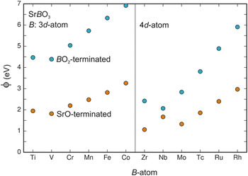
• The output voltage is limited by the work function difference between the emitter and collector electrodes. Although existing materials are adequate for good performance, materials designed for targeted work functions are advantageous. In particular, collector materials with work functions of 0.5–1.2 eV are desirable for most applications. This affords great opportunities for materials science. Work functions are commonly highly sensitive to a material’s surface properties. In simple perovskites, for example, surface termination may alter the work function by several electron volts. Reference Zhong and Hansmann36 Figure 6 shows the work function of a SrBO3 perovskite (B = 3d, 4d elements) calculated by density functional theory (generalized gradient approximation) for SrO and BO2 surface termination. Reference Zhong and Hansmann36 Note that, for example, the work function of SrRuO3 is found to be ∼4.9 eV for RuO2 termination, but only ∼2.4 eV for SrO termination. Heterostructure growth offers possibilities to engineer work functions as well as the infrared emissivities. It is relevant to control the diffusion processes and defect formation to achieve sufficiently long lifetimes at high operation temperatures. Surface structuring provides further options to enhance electron emission and absorption, through, for example, small and sharp structures that enhance the electric field locally and therefore increase the electron current.
-
• Although even a rather low vacuum (1 Pa) is sufficient to ensure the required electron mean free path exceeds the electrode spacing, the vacuum also serves to prevent surface contamination and to provide thermal insulation. For the latter, vacuum greater than 10−2–10−3 Pa is needed. Converter design and the choice of materials determine the vacuum quality required for a specific application. Although radio tubes operate at lower temperatures than most thermoelectronic converters, it is encouraging that they have sustained equivalent vacuum levels for decades, Reference Tyne19 a property that is also required for thermoelectronic energy converters.
-
• For fabricating converters, the use of nanovacuum electronics technologies appears promising. Reference Lee, Bargatin, Vancil, Gwinn, Maboudian, Melosh and Howe14 For example, we envision the modular use of wafers mounted in a flip-chip technology. Thermal insulation, electrode alignment, and contacts are technological issues. Large-scale units comprising numerous stacked wafers could be driven by magnetic fields generated by high-Tc superconducting coils. Using 2D materials as gates will be preferable for small, mobile converters.
-
• Thermoelectronic and thermionic energy conversion face technological issues of an engineering nature, which raises intriguing materials science questions. We have not (yet) been able to identify fundamental impediments, but it is still too early to consider applications seriously, since high efficiencies have yet to be achieved. Nevertheless, as widely recognized in the literature, Reference Meir, Stephanos, Geballe and Mannhart3 obvious exciting fields of applications do exist, for example, the use in topping cycles of conventional heat-conversion processes such as steam turbines or as converters of high temperatures (see Figure 4). Such systems are of interest for use in focused solar-energy and coal-combustion plants. Owing to the large-scale global use of fossil-fuel energy, even a small efficiency gain would directly lead to a significant reduction of CO2 emissions. Other possible applications include burning fuel to generate electricity for vehicles or to supply rural areas. Related applications are currently being pursued by at least two startup companies. 38,39
Work functions (ϕ) of a perovskite ABO3 series with A = Sr and B (x-axis) being a 3d (left) or 4d (right) element for AO (orange) and BO2 (blue) surface termination calculated by density functional theory. Reference Lee, Bargatin, Melosh and Howe16 Perovskites show a large variety of work function with a high level of controllability.

Summary, outlook, and possible applications
Thermoelectronic energy conversion is a promising approach for highly energy-efficient conversion of heat into electricity. We have not been able to identify fundamental impediments to achieving high efficiencies. However, serious technological problems must be overcome, such as reducing gate, ohmic, and infrared losses or mounting aligned electrodes operating at a temperature difference of many hundreds of degrees centigrade at a spacing on the order of 100 μm. Although today’s materials are already capable of driving a number of applications, it will be increasingly desirable to engineer materials with specific and low work functions for use as emitter and collector electrodes. High conversion efficiencies must also be demonstrated experimentally.
Acknowledgments
We gratefully acknowledge productive collaborations and discussions with G. Gassler, T.H. Geballe, P. Hansmann, G. Hassink, S. Meir, C. Stephanos, and Z. Zhong. A. Kyriazis thanks the Max Planck–UBC Center for Quantum Materials for support. This work was supported by the DFG (Leibniz-Preis program).

Robin Wanke is a doctoral candidate in the Department of Solid State Quantum Electronics at the Max Planck Institute for Solid State Research, Germany. He received his master’s degree in physics from the University of Stuttgart, Germany, in 2014. His research interests include energy conversion, high temperatures, ultrahigh vacuum technology, thin-film growth, microstructuring, and high pressures. Wanke can be reached by email at r.wanke@fkf.mpg.de.

Wolfgang Voesch is a doctoral candidate in the Department of Solid State Quantum Electronics at the Max Planck Institute for Solid State Research, Germany. He studied physics at the University of Western Australia, and the University of Stuttgard, Germany, where he received his master’s degree in 2015. His research interests include thin-film growth with pulsed laser deposition, surface science, work-function engineering, and thermoelectronic energy conversion. Voesch can be reached by email at w.voesch@fkf.mpg.de.

Iman Rastegar Alam joined the Department of Solid State Quantum Electronics at the Max Planck Institute for Solid State Research, Germany, in 2011. He received his master’s degree in 2012 from the University of Stuttgart, Germany, where he investigated the defect chemistry of Ti thin films and applications in future memory storage. His research interests include vacuum electronics, thin-film growth, and energy storage. Rastegar Alam can be reached by email at i.rastegar@fkf.mpg.de.

Alex Kyriazis is an undergraduate engineering physics student from The University of British Columbia, Canada. He has conducted research with the thermoelectronics group at the Max Plank Institute for Solid State Research, Germany. His research focuses on engineering design for improving heating efficiencies in ultrahigh vacuum, high-temperature environments. Kyriazis can be reached by email at alexander.kyriazis@alumni.ubc.ca.

Wolfgang Braun is a researcher in the Department of Solid State Quantum Electronics at the Max Planck Institute for Solid State Research, Germany. He studied physics at the University of Stuttgart, Germany, and the Georgia Institute of Technology, and obtained his PhD degree from Humboldt University, Germany, in 1996. His research interests include energy conversion and storage, ultrahigh vacuum technology and high temperatures, crystal growth, and in situ diffraction studies. Braun can be reached by email at w.braun@fkf.mpg.de.

Jochen Mannhart has been a director at the Max Planck Institute for Solid State Research, Germany, and head of the institute’s Department of Solid State Quantum Electronics since 2011. He studied physics at the University of Tübingen, Germany. He worked as a visiting scientist at the IBM T.J. Watson Research Center, and as a research staff member at the IBM Research Laboratory, Switzerland. From 1996 to 2011, he was a professor at Augsburg University, Germany. He has received numerous awards for his research, including the Gottfried Wilhelm Leibniz-Preis and the Europhysics Prize. Mannhart can be reached by email at office-mannhart@fkf.mpg.de.