





Introduction
Achieving the high data rates and low latency targets of next-generation communication and sensing systems calls for large-scale D-band (110–170 GHz) antenna arrays featuring highly directive beams and wide bandwidths [Reference de Kok, Smolders and Johannsen4]. Such D-band arrays generally exploit either printed circuit board (PCB)-based technologies [Reference Manzillo1–Reference Hamani3] or low-loss waveguide-based approaches such as rectangular waveguide (RWG), commonly fabricated through CNC milling [Reference Tan, Xiao, Li, Zhu, Luo and Sun5], 3D printing [Reference Li6], or silicon micromachining [Reference Gomez-Torrent7]. While PCB-based implementations offer a compact and integration-friendly solution, their higher intrinsic losses limit the achievable efficiency for large, high-gain arrays. In contrast, RWG-based implementations provide superior efficiency, but are less suited for compact integration with active circuitry. As a result, hybrid configurations are often preferred for such applications [Reference Peeters8], in which integrated circuits (ICs) are mounted on a PCB platform through flip-chip or wirebond interconnections. Consequently, efficient and broadband transition structures become essential to interconnect the PCB-mounted components with the RWG-based antenna arrays.
Such PCBs must accommodate numerous control and power interconnects required for operating the associated electronics, resulting in carrier architectures composed of multiple thin substrate layers [Reference Vosoogh9]. End-launch PCB-to-RWG transitions [Reference Zhang, Shi, Martin and Prather10, Reference Hassona, He, Vassilev and Zirath11] offering a broad impedance bandwidth can be realized on these multilayer carriers, while utilizing only a limited number of layers. However, these transitions inherently occupy a large lateral area, leading to bulky assemblies and often necessitating a split-block configuration [Reference Zhang, Shi, Martin and Prather10, Reference Li, Tong and Niu12] or augmentation of the waveguide implementation through adaptations such as stepped impedance structures [Reference Pérez, Rebollo, Gonzalo and Ederra13]. As an alternative, vertical-launch transition topologies [Reference Zhang, Huang, Zhou, Huang and Zhang14–Reference Hafeez-Ur-Rehman, Song, Park and Jang18, Reference Seo, Sakakibara and Kikuma20–Reference Li and Dou22] enable more compact integration, though none currently achieve full D-band coverage. To realize a high-performance and versatile D-band interface between RWG and PCB in heterogeneous integration platforms, a transition design that combines compactness, broad bandwidth, and robustness is critical.
We propose a superstrate-based RWG-to-substrate-integrated-waveguide (SIW) transition, which is the first to cover the entire D-band. This is achieved by co-optimizing two resonators, a slot and a patch, with a dielectric-loading superstrate, resulting in a measured -10dB-impedance bandwidth of 108–173GHz (a fractional bandwidth (FBW) of 46%) and an insertion loss (IL) of only (0.95 $\pm$0.15) dB, which is the lowest currently found at D-band. The presented transition was initially reported in [Reference Rimbaut, Kapusuz, Rogier and Lemey25], where the superstrate-based concept and corresponding measurement results were first introduced. However, that work was limited to demonstrating the concept and did not provide a detailed analysis of the underlying operating mechanisms nor a systematic investigation of the design parameters. An earlier version of this paper was presented at EuMW 2025 and was published in its proceedings [Reference Rimbaut, Kapusuz, Rogier and Lemey23]. Yet, in this contribution, we provide a deeper analysis of the previously proposed transition by introducing an equivalent circuit model that not only explains its underlying operating mechanisms, but also provides a means to estimate the optimal resonance frequencies of the patch and slot, as well as the optimal superstrate height. Next, we examine the robustness achieved by the superstrate-based approach to account for the tight design tolerances inherent to standard multi-layer high-density interconnect (HDI) PCB fabrication at D-band. In addition, the proposed transition does not require depth routing, ensuring compatibility with standard PCB manufacturing processes. Variations in other relevant design parameters are also investigated, demonstrating the topology’s resilience to the full range of expected tolerances. Furthermore, several prototypes have been measured, providing experimental evidence of the robustness of the proposed superstrate-based transition.
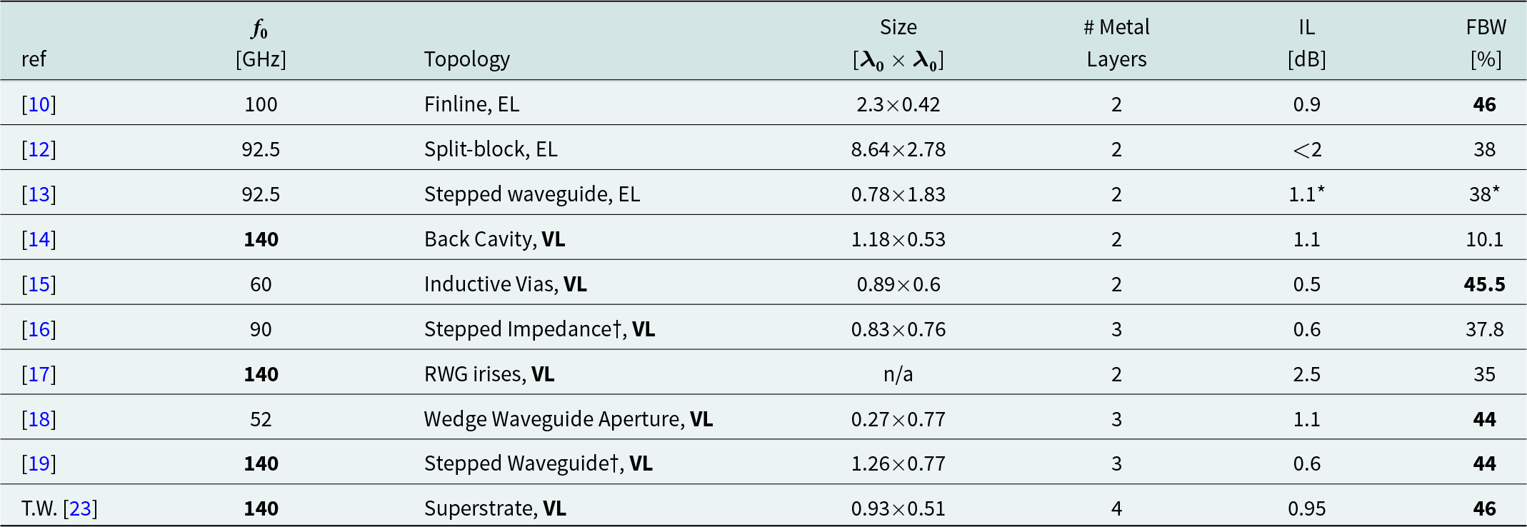
In the literature, several wideband vertical-launch RWG-to-planar-waveguide transitions have been reported. These approaches also employ aperture coupling: the on-PCB SIW [Reference Mohamed and Sebak15, Reference Hansen and Pohl16] or microstrip [Reference Zhang, Huang, Zhou, Huang and Zhang14, Reference Schepers and Krebs17, Reference Hafeez-Ur-Rehman, Song, Park and Jang18] feed structure excites a resonant patch, which then couples to the RWG to realize wideband interfacing. However, achieving an impedance match across the full D-band (FBW $\ge$43%) requires additional matching elements in such configurations. In [Reference Mohamed and Sebak15], inductive via posts are introduced to control the matching bandwidth. However, relying on the precise placement of a single via makes the transition sensitive to fabrication tolerances at D-band. In [Reference Hansen and Pohl16], broadband performance is obtained using depth routing to form a stepped-impedance SIW section, which enhances bandwidth but adds design complexity due to the need for accurate depth control. Similarly, [Reference Braun, Romstadt, Hansen, Schweer and Pohl19] deploys depth routing to create a stepped impedance waveguide, along with an additional substrate taper to create a RWG-to-differential microstrip transition that covers the full D-band. The D-band transition in [Reference Zhang, Huang, Zhou, Huang and Zhang14] relies on an aperture and a back cavity. Measurements align well with simulations, indicating good tolerance robustness, though the structure still falls short of full D-band coverage. In [Reference Schepers and Krebs17], a microstrip-to-RWG transition achieves an FBW of 35% by incorporating irises into the RWG. This approach reduces on-PCB complexity, requires custom RWG sections, and results in higher IL. [Reference Hafeez-Ur-Rehman, Song, Park and Jang18] implements a microstrip-to-RWG structure based on a probe and resonant patch to achieve an FBW of 44% at an operating frequency of 52GHz. The design counters RWG-to-PCB misalignment and improves matching through a wedge-shaped waveguide. Although its IL is higher than that of the solution presented here, which enhances robustness using only a standard WR-06 waveguide, the wedge-shaped approach is compatible with this work, and combining both strategies can be considered. These works are summarized in Table 1.
Performance of state-of-the-art millimeter-wave RWG-to-PCB transitions

Table 1 Long description
Columns list reference, center frequency in gigahertz, topology, size in free space wavelength by free space wavelength, number of metal layers, insertion loss in decibels, and fractional bandwidth in percent. Reference 10 reports 100 gigahertz finline end launch, size 2.3 by 0.42, 2 metal layers, insertion loss 0.9, fractional bandwidth 46. Reference 12 reports 92.5 gigahertz split block end launch, size 8.64 by 2.78, 2 layers, insertion loss less than 2, fractional bandwidth 38. Reference 13 reports 92.5 gigahertz stepped waveguide end launch, size 0.78 by 1.83, 2 layers, insertion loss 1.1 marked with an asterisk, fractional bandwidth 38 marked with an asterisk. Reference 14 reports 140 gigahertz back cavity vertical launch, size 1.18 by 0.53, 2 layers, insertion loss 1.1, fractional bandwidth 10.1. Reference 15 reports 60 gigahertz inductive vias vertical launch, size 0.89 by 0.6, 2 layers, insertion loss 0.5, fractional bandwidth 45.5. Reference 16 reports 90 gigahertz stepped impedance vertical launch, size 0.83 by 0.76, 3 layers, insertion loss 0.6, fractional bandwidth 37.8. Reference 17 reports 140 gigahertz RWG irises vertical launch, size not provided, 2 layers, insertion loss 2.5, fractional bandwidth 35. Reference 18 reports 52 gigahertz wedge waveguide aperture vertical launch, size 0.27 by 0.77, 3 layers, insertion loss 1.1, fractional bandwidth 44. Reference 19 reports 140 gigahertz stepped waveguide vertical launch, size 1.26 by 0.77, 3 layers, insertion loss 0.6, fractional bandwidth 44. T. W. 23 reports 140 gigahertz superstrate vertical launch, size 0.93 by 0.51, 4 layers, insertion loss 0.95, fractional bandwidth 46.
[†] indicates depth routing, EL = End-Launch, VL = Vertical-Launch, * indicates simulation
In the “Transition operation and modeling” section, we analyze the operation of the transition component provided previously in [Reference Rimbaut, Kapusuz, Rogier and Lemey23, Reference Rimbaut, Kapusuz, Rogier and Lemey25] by means of an equivalent circuit model. In the “Robust full D-band superstrate-based RWG-to-SIW transition” section, our proposed superstrate-based approach is compared to an alternative structure that omits the superstrate, underpinning its superior robustness against fabrication tolerances. The “Experimental validation” section explains the validation approach, including the measurement setup and S-parameter measurements of several fabricated prototypes, which are compared to the simulation results. Finally, the “Conclusion section” concludes the paper.
Transition operation and modeling
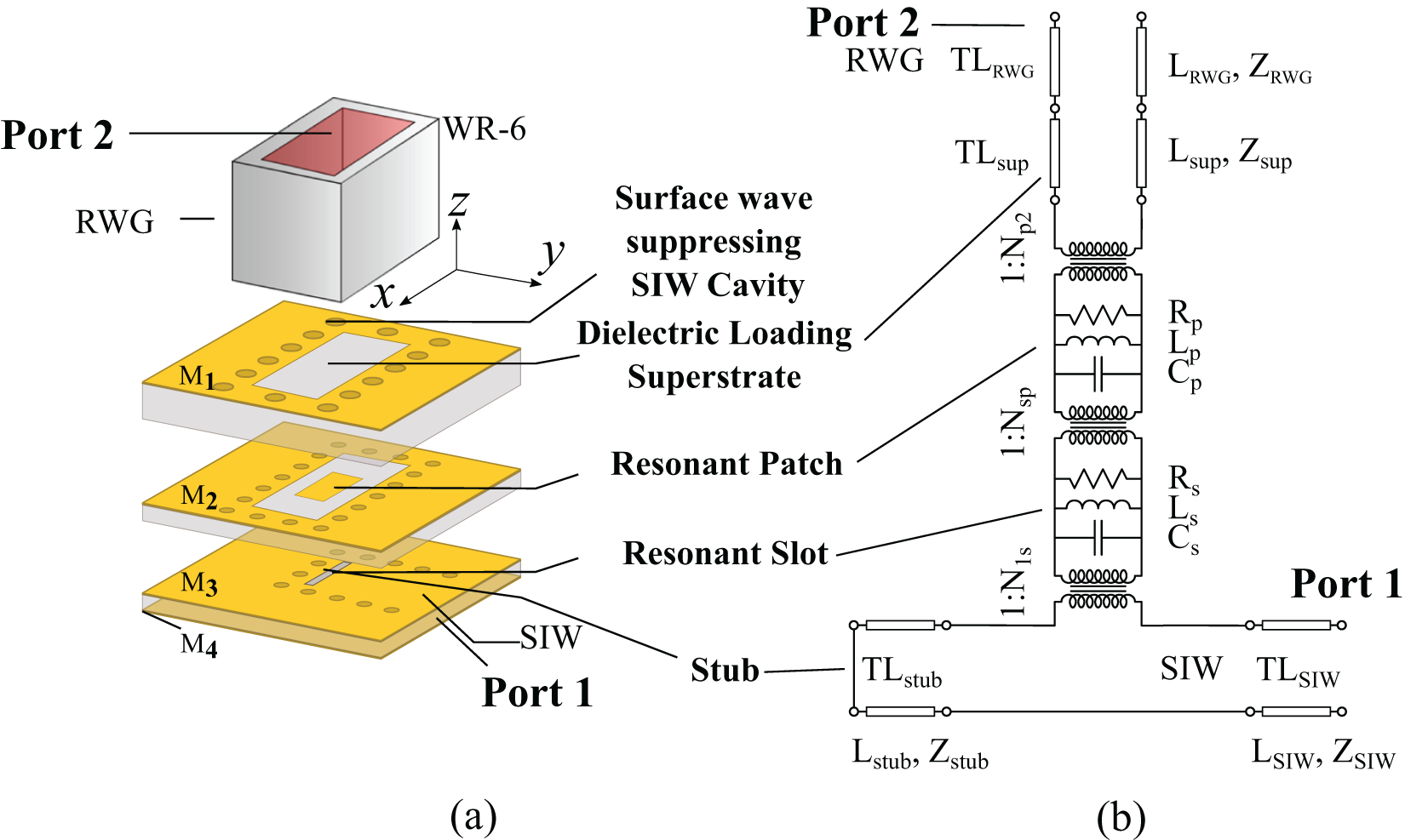
To realize an interfacing component that enables efficient RWG-to-PCB interconnection for next-generation communication and sensing systems operating across the entire D-band, a wideband and low-loss design is essential. In this work, we introduce an RWG-to-SIW transition that exploits a resonant slot–patch configuration, further enhanced by incorporating a dielectric-loading superstrate, consisting of Megtron 7 R-5680(N) [26] dielectric material, to achieve the target performance [Reference Rimbaut, Kapusuz, Rogier and Lemey23]. The combined slot and patch resonances provide the required wideband characteristics, while the dielectric superstrate ensures that these resonances fall within the D-band. Crucially, the superstrate significantly enhances the structure’s resilience to PCB fabrication tolerances. The proposed component is depicted in Fig. 1(a).
(a) Proposed topology in [Reference Rimbaut, Kapusuz, Rogier and Lemey23] and (b) Equivalent circuit model containing the coupling mechanisms discussed in [Reference Rimbaut, Kapusuz, Rogier and Lemey23, Reference Rimbaut, Kapusuz, Rogier and Lemey25], which influence the resonances associated with the slot and patch resonators. The equivalent circuit parameters are given as follows:  $\text{L}_\text{SIW}~=~{1}\,\mathrm{mm}$,
 $\text{Z}_\text{SIW}~=~{265}\,{\Omega}$,
 $\text{L}_\text{RWG}~=~{1}\,\mathrm{mm}$,
 $\text{Z}_\text{RWG}~=~{495}\,{\Omega}$,
 $\text{L}_\text{sup}~=~{0.147}\,{\text{mm}}$,
 $\text{Z}_\text{Sup}~=~{230}\,{\Omega}$,
 $\text{L}_\text{stub}~=~{0.1625}\,\mathrm{mm}$,
 $\text{Z}_\text{stub}~=~{263}\,{\Omega}$,
 $\text{N}_\text{1s}~=~1.29$,
 $\text{N}_\text{sp}~=~0.98$,
 $\text{N}_\text{p2}~=~0.83$,
 $\text{R}_\text{s}~=~{5}\,\mathrm{k}\Omega$,
 $\text{L}_\text{s}~=~{0.39}\,\mathrm{nH}$,
 $\text{C}_\text{s}~=~{0.11}\,{fF}$,
 $\text{R}_\text{p}~=~{100}\,\mathrm{k}\Omega$,
 $\text{L}_\text{p}~=~{0.98}\,\mathrm{nH}$ and
 $\text{C}_\text{p}~=~{2.8}\,\mathrm{fF}$.

Figure 1 Long description
The image consists of two parts. The first part on the left illustrates a proposed topology for RWG-to-PCB interconnection. It features a three-dimensional view of a structure with multiple layers labeled M1, M2, M3 and M4. At the top is a rectangular waveguide labeled WR-6, connected to Port 2. Below it, the layers are labeled as Surface wave suppressing SIW Cavity, Dielectric Loading Superstrate, Resonant Patch and Resonant Slot, leading to Port 1. The second part on the right is an equivalent circuit model. It shows a series of transmission lines and components. Port 2 is connected to a transmission line labeled TL subscript RWG, with inductance and impedance labeled L subscript RWG and Z subscript RWG. This connects to a series of transformers and resonant components, including inductors and capacitors labeled R subscript p, L subscript p, C subscript p, R subscript s, L subscript s and C subscript s. The circuit ends at Port 1, connected through a stub and SIW transmission line labeled TL subscript SIW, with inductance and impedance labeled L subscript SIW and Z subscript SIW.
The proposed RWG-to-SIW transition exploits three main components: a resonant slot ( $\text{M}_\text{3}$), a resonant patch (
 $\text{M}_\text{2}$), and a dielectric superstrate, whose behavior can be directly mapped to the equivalent circuit model depicted in Fig. 1(b). In this model, the slot and patch are represented by RLC resonators, while the superstrate is modeled as a short RWG section. The coupling mechanisms responsible for the transition operation (SIW-slot coupling, slot–patch coupling, and patch–RWG coupling) are explicitly included as transformer components. Physically, the slot couples the
 $\text{TE}_\text{10}$ mode of the SIW section, dimensioned for a cut-off frequency
 $\text{f}_\text{c}$ = 85GHz to ensure in-band linear-phase behavior [Reference Bozzi24], to the
 $\text{TM}_\text{100}$ resonant mode below the patch, which then interfaces with the RWG’s
 $\text{TE}_\text{10}$ mode.
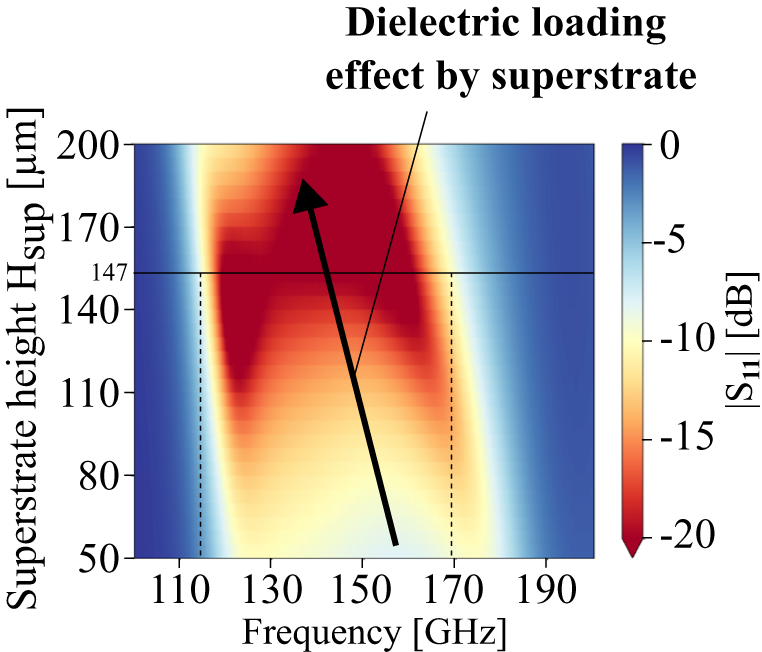
The superstrate is tuned using the equivalent circuit model to optimally position both resonances within the D-band. This step is essential, as the slot alone cannot be made sufficiently long inside the SIW to achieve an in-band resonance without dielectric loading, as shown previously in [Reference Rimbaut, Kapusuz, Rogier and Lemey25]. The effects of varying the superstrate height, thus affecting the dielectric loading, are illustrated in Fig. 2. Increasing the superstrate height shifts the band of operation downward in frequency, allowing for D-band coverage with the resonant slot-patch pair. From this simulation, a superstrate height  $\text{H}_\text{sup} = {147}\, {\unicode{x03BC}{m}}$ is selected.
Magnitude of the reflection coefficient in dB, as a function of frequency and superstrate height, based on the proposed equivalent circuit. Increasing the superstrate height shifts the operating band downward. An optimal superstrate height of  $\text{H}_\text{sup} = {147}\,\mu \mathrm{m}$ is selected to maximize D-band coverage.

Figure 2 Long description
Dielectric loading effect by superstrate. A heatmap with a horizontal axis labeled, Frequency, with unit gigahertz. Tick labels shown are 110, 130, 150, 170 and 190. The plotted frequency span shown is from 100 to 200 gigahertz. A vertical axis labeled, Superstrate height Hsup, with unit micrometer. Tick labels shown are 50, 80, 110, 140, 170 and 200. The plotted superstrate height span shown is from 50 to 200 micrometer. A vertical scale bar is labeled, vertical bar S11, with unit decibel. Tick labels shown on the scale are 0, minus 5, minus 10, minus 15 and minus 20. The scale bar shows 0 at the top and minus 20 at the bottom. A solid horizontal line crosses the heatmap at the y value labeled 147. Two vertical dashed lines cross the heatmap: one near the x value slightly above 110 gigahertz and one at the x value labeled 170 gigahertz. A thick arrow starts near 160 gigahertz and a superstrate height slightly above 50 micrometer and ends near 135 gigahertz and a superstrate height near 190 micrometer. A thin diagonal line starts near the arrow tail region and extends upward toward the title. The lowest scale values, near minus 20 decibel, appear in a broad central band between about 120 and 170 gigahertz, with the darkest region concentrated around about 140 to 160 gigahertz and superstrate heights around about 140 to 200 micrometer. Values closer to 0 decibel appear near the left and right edges of the frequency range, around 100 to 115 gigahertz and around 180 to 200 gigahertz, across most superstrate heights.
After establishing in-band operation, the resonance frequencies, the lower one governed by the patch width ( $\text{W}_\text{p}$) and the upper one by the slot length (
 $\text{L}_\text{s}$), are distributed over the D-band to maximize the bandwidth, with optimal resonance placements at 120 GHz and 157 GHz.
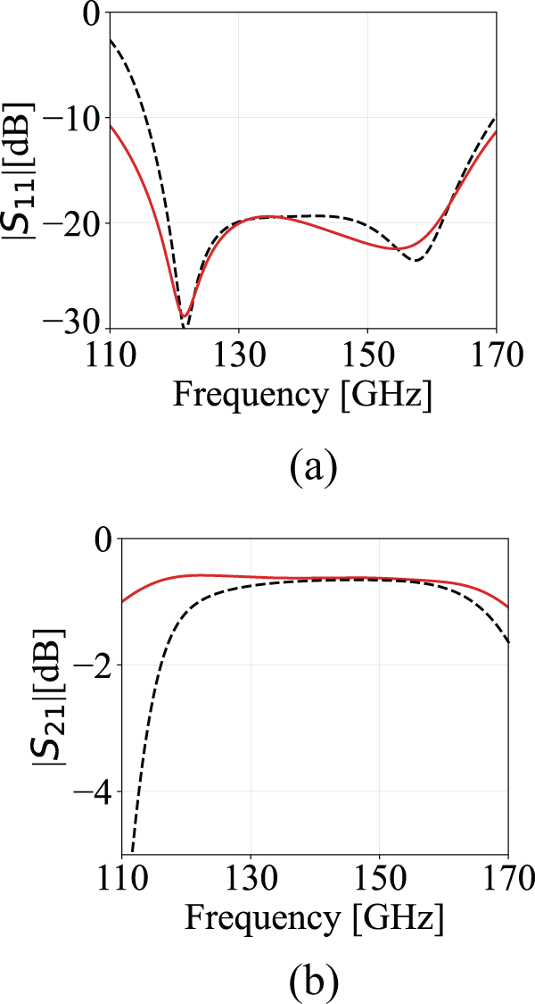
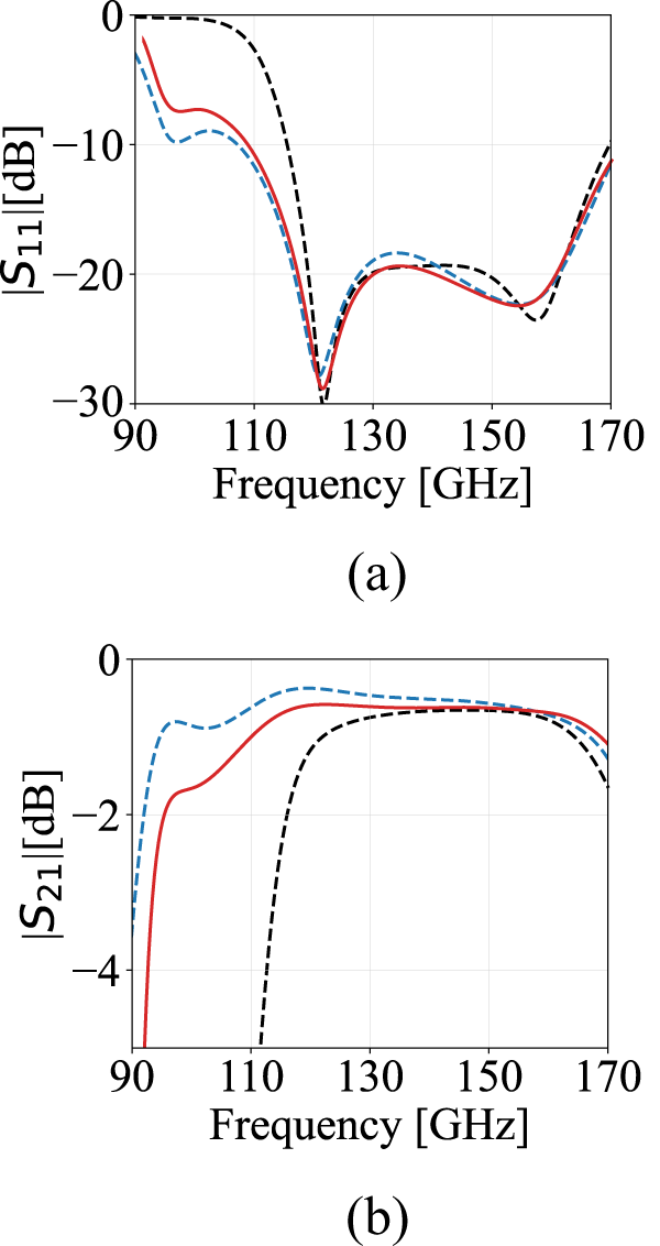
The reflection coefficient and insertion loss of the equivalent circuit are shown in Fig. 3. They are compared to a full-wave electromagnetic (EM) model, with the previously obtained  $\text{H}_\text{sup} = {147}\,\mu \mathrm{m}$, in the band of interest (110–170 GHz). Note that the aforementioned slot and patch resonances are indeed present in the equivalent circuit model as well as in the full-wave Em simulation. However, given that its results deviate from the EM simulation at the lower end of the band, the equivalent circuit model no longer captures the detailed behavior of the transition in this frequency range. Despite this, the model provides valuable insight into the operation of the RWG-to-SIW transition. Moreover, it has proven highly effective for obtaining an initial parameter estimation, specifically the aforementioned superstrate height. To obtain more accurate predictions across the full 110–170 GHz band, a more comprehensive equivalent circuit is required.
(a) Reflection coefficient and (b) insertion loss of the simple equivalent circuit from Figure 1(b) (black dashed curve) and full-wave simulation (red curve). The existence of the in-band resonances is correctly predicted. However, the model is less accurate at the lower end of the band due to missing additional coupling mechanisms not modeled by the initially proposed equivalent circuit.

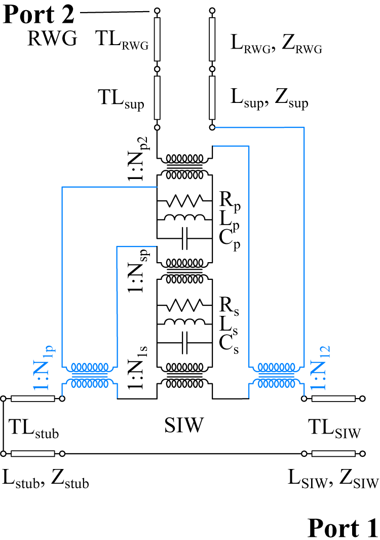
Using the parameters obtained from the simplified model as a starting point, we introduce the advanced equivalent circuit shown in Fig. 4, which incorporates additional parasitic coupling paths that influence the bandwidth of the insertion loss. These added elements represent direct coupling between the SIW and the patch, and between the SIW and the RWG (both occurring via the slot). These effects were not included in the simpler model. By accounting for these mechanisms through curve fitting of the advanced model to the full-wave EM results, the behavior shown in Fig. 5 is obtained. An additional resonance, absent in the initial equivalent circuit model, is now accurately captured, resulting in excellent agreement with the full-wave EM simulation. The insertion loss predicted by the advanced equivalent circuit model also closely follows the EM results, providing nearly identical in-band performance over 110–170 GHz.
Advanced equivalent circuit modeling additional parasitic coupling mechanisms representing direct coupling between the SIW and the patch, and between the SIW and the RWG. These additional elements are indicated in blue. The updated circuit parameters are given by:  $\text{L}_\text{SIW}~=~{1}\,\mathrm{mm}$,
 $\text{Z}_\text{SIW}~=~{265}\,{\Omega}$,
 $\text{L}_\text{RWG}~=~{1}\,\mathrm{mm}$,
 $\text{Z}_\text{RWG}~=~{495}\,{\Omega}$,
 $\text{L}_\text{sup}~=~{0.147}\,\mathrm{mm}$,
 $\text{Z}_\text{Sup}~=~{230}\,{\Omega}$,
 $\text{L}_\text{stub}~=~{0.1625}\,\mathrm{mm}$,
 $\text{Z}_\text{stub}~=~{263}\,{\Omega}$,
 $\text{N}_\text{1s}~=~1.52$,
 $\text{N}_\text{sp}~=~1.43$,
 $\text{N}_\text{p2}~=~0.73$,
 $\text{N}_\text{1p}~=~0.86$,
 $\text{N}_\text{12}~=~1.85$,
 $\text{R}_\text{s}~=~{5}\,\mathrm{k}\Omega$,
 $\text{L}_\text{s}~=~{0.46}\,\mathrm{nH}$,
 $\text{C}_\text{s}~=~{0.11}\,\mathrm{fF}$,
 $\text{R}_\text{p}~=~{100}\,\mathrm{k}\Omega$,
 $\text{L}_\text{p}~=~{0.98}\,\mathrm{nH}$ and
 $\text{C}_\text{p}~=~{2.6}\,\mathrm{fF}$.

Figure 4 Long description
An advanced equivalent circuit model with various components and connections. At the top, Port 2 is labeled RWG, connected to transmission lines TL subscript RWG and TL subscript sup. These lines are connected to inductors L subscript RWG and L subscript sup and impedances Z subscript RWG and Z subscript sup. Below these, a transformer with a ratio of 1:N subscript p2 is connected to a parallel RLC circuit consisting of resistor R subscript p, inductor L subscript p and capacitor C subscript p. Another transformer with a ratio of 1:N subscript sp is connected to a similar RLC circuit with components labeled R subscript s, L subscript s and C subscript s. The circuit includes additional transformers with ratios 1:N subscript lp and 1:N subscript ls, connected to the SIW section. The SIW section is connected to transmission lines TL subscript stub and TL subscript SIW, with inductors L subscript stub and L subscript SIW and impedances Z subscript stub and Z subscript SIW. Port 1 is located at the bottom of the diagram. The circuit is designed to model parasitic coupling mechanisms between the SIW and other components, enhancing bandwidth and insertion loss characteristics.
(a) Reflection coefficient and (b) insertion loss of the simple equivalent circuit from Figure 1(b) (black dashed curve), advanced equivalent circuit from Figure 4 (blue dashed curve), and full-wave simulation (red curve). The [90–110 GHz] range is included to highlight the additional out-of-band resonance introduced by parasitic coupling mechanisms, which is captured only by the advanced circuit model.

Note that, while the coupling level between the resonators needed to be tuned to match the response of the advanced equivalent circuit, the parameters of the slot, patch, stub, and superstrate remain effectively unchanged. In particular, the superstrate height and the stub length retain the same values in both the physical implementation (EM-model) and the equivalent circuit representations, thereby showcasing physical significance and simplifying the curve-fitting procedure.
In summary, the simplified equivalent circuit serves as an efficient tool for conceptualizing the transition operation and for rapidly estimating key design parameters such as the in-band resonance frequencies and the required superstrate height. Building on this foundation, the advanced equivalent circuit offers a higher level of accuracy by incorporating additional coupling mechanisms. While being more intricate and therefore less suited for initial optimization, this advanced model reliably reproduces the full-wave EM behavior across the entire D-band. It is thus well-suited for providing a more detailed understanding of the operating mechanisms of the proposed component.
Robust full D-band superstrate-based RWG-to-SIW transition
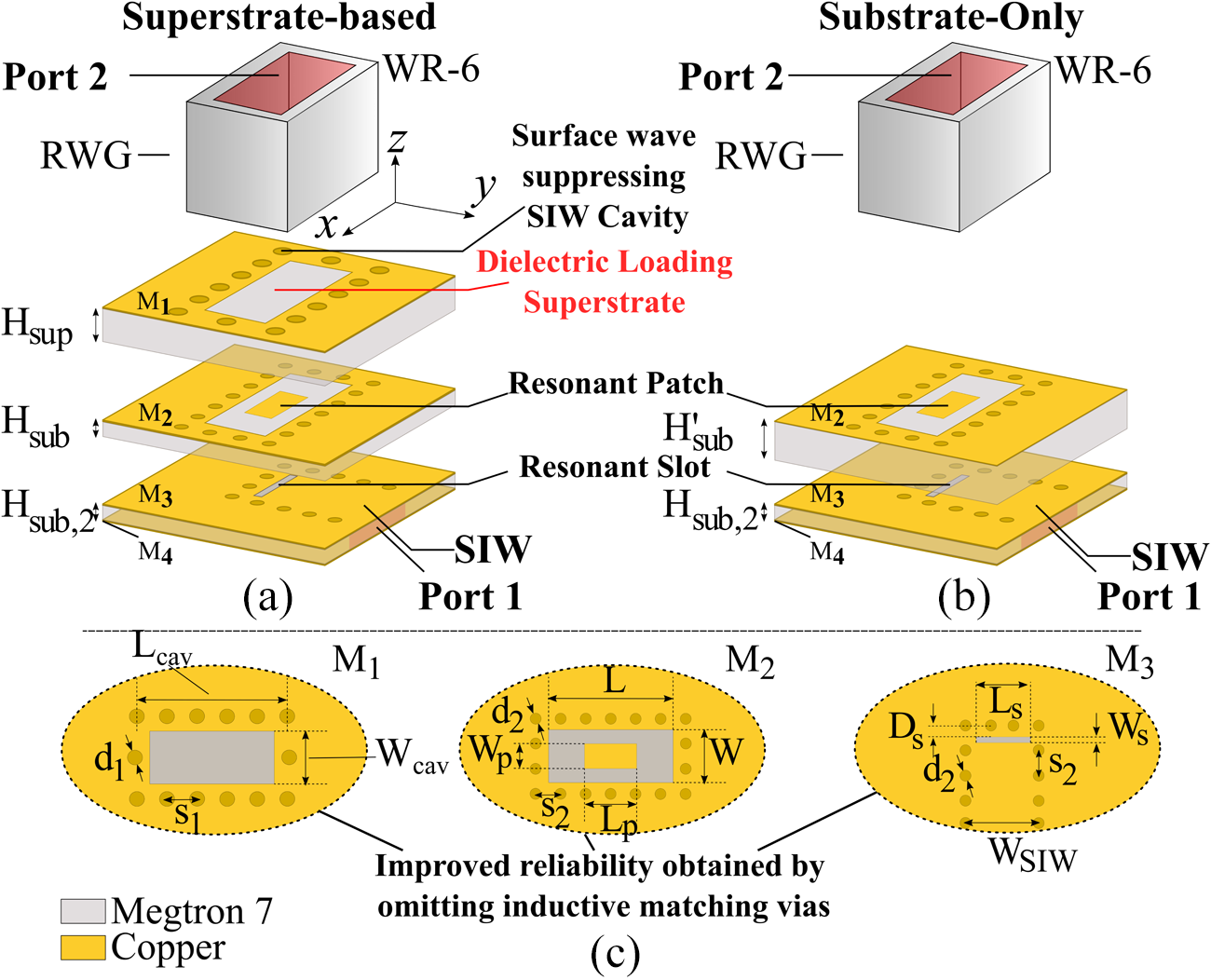
We now compare the proposed transition with an alternative approach for achieving in-band operation through dielectric loading. The benchmark topology, shown in Fig. 6(b), implements this by increasing the substrate height  $\text{H'}_\text{sub}$ rather than by introducing the superstrate layer (similar to, e.g., [Reference Li and Luk21]) as in the proposed design. Functionally, this alternative component behaves similarly to the structure analyzed in the previous section, but with dielectric loading governed by the thicker substrate instead of the superstrate height
 $\text{H}_\text{sup}$. Fig. 6 summarizes both configurations: in-band operation is achieved either using the superstrate-based solution (
 $\text{H}_\text{sup}$, Fig. 6(a)) or by relying on a thicker substrate (
 $\text{H'}_\text{sub}$, Fig. 6(b)).
Geometry of the proposed RWG-to-SIW transition employing a resonant patch and slot, co-optimized with (a) a thin dielectric substrate layer ( $\text{H}_\text{sub}$) with additional superstrate layer (
 $\text{H}_\text{sup}$) and (b) a thick dielectric substrate layer (
 $\text{H'}_\text{sub}$) without additional superstrate layer to place both resonances within the D-band and ensure full D-band operation. An SIW cavity is included to suppress surface wave propagation. (c) includes the remaining transition parameters. Final dimensions of the superstrate-based/substrate-only design:
 $\text{L}_\text{cav}$ = 2 mm/2 mm,
 $\text{W}_\text{cav}$ = 1.1 mm/0.93 mm, L = 1.65 mm/1.65 mm, W = 0.7 mm/0.525 mm,
 $\text{L}_\text{p}$ = 0.7 mm/0.65 mm,
 $\text{W}_\text{p}$ = 0.32 mm/0.25 mm,
 $\text{d}_1$ = 0.2 mm/0.2 mm,
 $\text{s}_1$ = 0.4 mm/0.4 mm,
 $\text{d}_2$ = 0.15 mm/0.15 mm,
 $\text{s}_2$ = 0.3 mm/0.3 mm,
 $\text{L}_\text{s}$ = 0.725 mm/0.735 mm,
 $\text{W}_\text{s}$ = 0.075 mm/0.075 mm,
 $\text{W}_\text{SIW}$ = 1.05 mm/1.05 mm,
 $\text{D}_\text{s}$ = 0.125 mm/0.125 mm,
 $\text{H}_\text{sup}$ = 147
 $\unicode{x03BC}$m/-,
 $\text{H}_\text{sub}$ = 102
 $\mu$m/150
 $\unicode{x03BC}$m,
 $\text{H}_\text{sub,2}$ = 102
 $\unicode{x03BC}$m/102
 $\unicode{x03BC}$m. Megtron 7 substrate:
 $\epsilon_r$ = 3.2, tan
 $\delta$ = 0.005, copper surface roughness:
 $\text{R}_\text{a}$ = 300 nm.

Figure 6 Long description
Two configurations for RWG-to-SIW transitions are illustrated. On the left, labeled as superstrate-based, a resonant patch and slot are shown with a dielectric loading superstrate above a thin dielectric substrate. This setup includes a surface wave suppressing SIW cavity and is connected to Port 1 and Port 2, both labeled WR-6. On the right, the substrate-only design features a thicker dielectric substrate without a superstrate, also connected to Port 1 and Port 2. Below these, three detailed views labeled M1, M2 and M3 show specific dimensions and components, such as resonant slots and patches, with materials indicated as Megtron 7 and copper. The section labeled M2 highlights improved reliability by omitting inductive matching vias. Each configuration is designed to ensure full D-band operation, with the superstrate-based design employing an additional superstrate layer for dielectric loading, while the substrate-only design relies on increased substrate thickness.
When comparing both options, the substrate-only design offers a slight cost advantage, since it requires only three metal layers instead of the four needed for the superstrate-based approach. Meanwhile, both options result in a comparable bandwidth and IL. However, we now show that, once robustness, previously identified as a critical design criterion, is taken into account, the superstrate-based solution clearly outperforms its substrate-only counterpart.
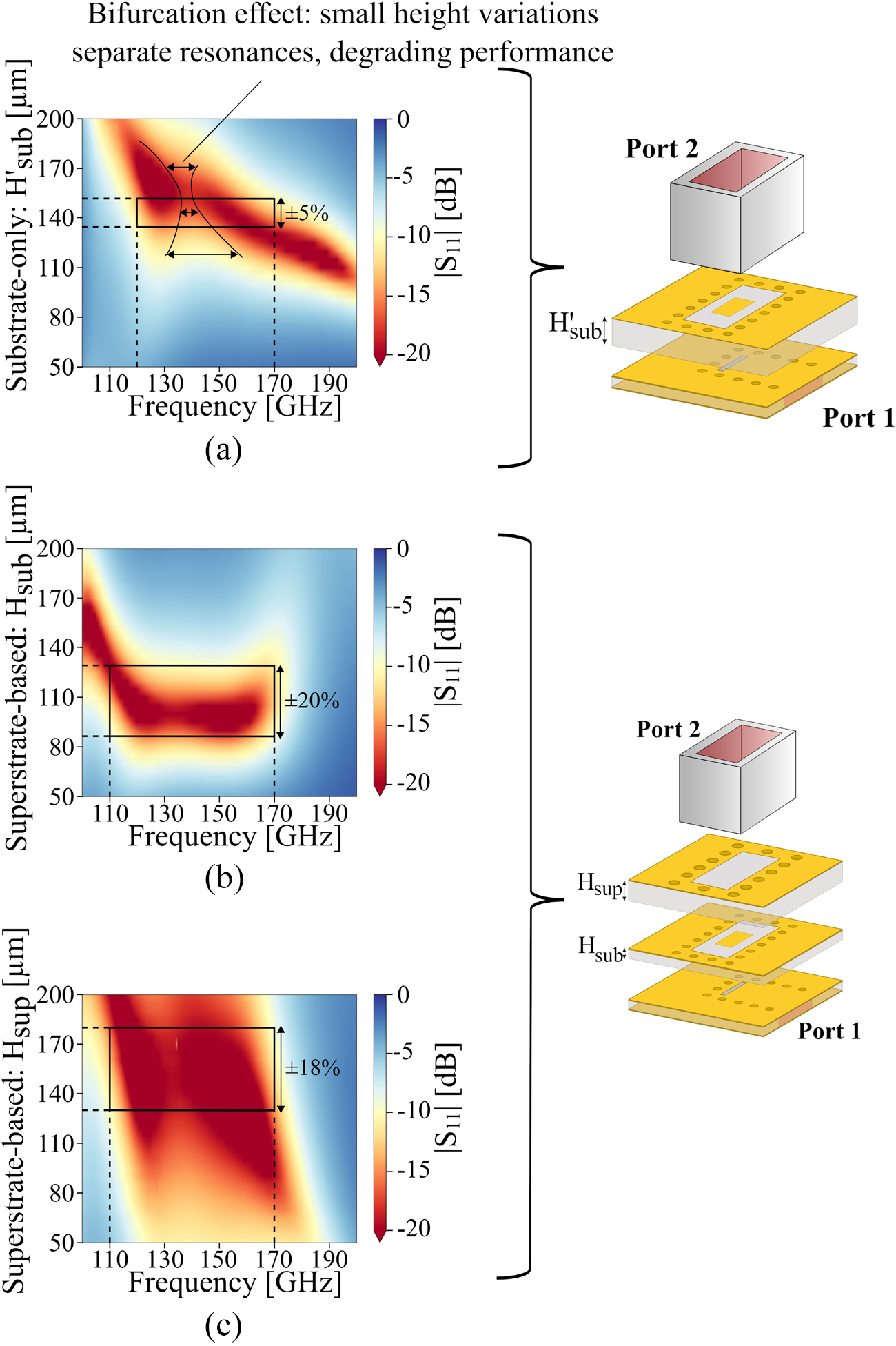
Fig. 7 presents an extensive variation analysis of the substrate and superstrate height parameters for both configurations, showing how these variations affect the transition’s frequency-dependent reflection coefficient. The results indicate that the superstrate-based design can accommodate variations up to  $\pm$20
 $\unicode{x03BC}$m (20%) in substrate height and
 $\pm$28
 $\unicode{x03BC}$m (18%) in superstrate height before losing full D-band coverage. In contrast, the substrate-only design already experiences bandwidth degradation for substrate height deviations as small as
 $\pm$7.5
 $\unicode{x03BC}$m (5%).
Magnitude of the reflection coefficient, in dB, as a function of frequency and of (a) the substrate height in the nominal substrate-only design, (b) the substrate height in the nominal superstrate-based design, and (c) the superstrate height in the nominal superstrate-based design. The region where the operating bandwidth is still covered, is indicated by the black boxes. The analysis demonstrates that the superstrate-based design is four times more robust against height variations of both substrate and superstrate.

Figure 7 Long description
Three heatmaps are arranged vertically, labeled (a), (b) and (c). All three share the same horizontal axis labeled Frequency in gigahertz, spanning 110 to 190 gigahertz. The vertical axis in each panel represents a height dimension in micrometers. The color scale in each panel ranges from 0 decibels at the upper end to minus 20 decibels or lower at the lower end, where lower decibel values indicate stronger reflection reduction. A black rectangular box is drawn on each heatmap to mark the region where the operating bandwidth remains covered. In (a), the vertical axis is labeled substrate-only H subscript sub in micrometers, ranging from approximately 110 to 170 micrometers. The black box spans a narrow height range and the annotation plus or minus 5 percent is marked. The region outside the black box shows a split or separation of the low-reflection zone into two distinct areas, indicating that small height changes disrupt the performance. The title text above reads: Bifurcation effect: small height variations separate resonances, degrading performance. In (b), the vertical axis is labeled superstrate-based H subscript sub in micrometers, ranging from approximately 80 to 170 micrometers. The black box spans a wider height range compared to (a) and the annotation plus or minus 20 percent is marked. The low-reflection zone remains more continuous across a broader height range, indicating greater tolerance. In (c), the vertical axis is labeled superstrate-based H subscript sup in micrometers, ranging from approximately 60 to 170 micrometers. The black box again spans a wide height range and the annotation plus or minus 18 percent is marked. The low-reflection zone similarly remains stable across a broad height range. Each panel is accompanied by a schematic diagram on the right side showing a layered structure with Port 1 at the bottom and Port 2 at the top, with the relevant height dimension labeled on the structure. Panels (b) and (c) share the same schematic showing both H subscript sup and H subscript sub layers stacked between the two ports.
Note that  $\text{H'}_\text{sub}$ not only controls the dielectric load on the slot and patch resonators, but also directly determines their physical separation. Because the coupling level between these resonators depends on this separation, variations in
 $\text{H'}_\text{sub}$ introduce an additional bifurcation effect affecting the resonance frequencies, ultimately reducing robustness. When a superstrate is used, however, these mechanisms, dielectric loading and mode bifurcation, remain decoupled, as illustrated in Fig. 7(b) and 7(c), respectively. An analogous result is obtained when varying the dielectric constants of the respective dielectrics; the superstrate-based structure shows superior tolerance against variations in dielectric constant.
This is further supported by the equivalent circuit model, where the aforementioned effects are modeled through variations in the  $\text{L}_\text{sup}$ and
 $\text{N}_\text{sp}$ parameters that affect the dielectric loading and mode bifurcation, respectively. If no superstrate is included in the model, these effects cannot be decoupled.
The insertion loss is virtually the same for both topologies, with simulations showing an in-band value of approximately 0.65 dB, when considering an average copper surface roughness  $\text{R}_a$ = 300 nm. This confirms that adding a superstrate layer does not introduce any meaningful loss. Additionally, the bandwidth of the superstrate-based design is slightly higher, covering the entire D-band (110–170 GHz). Meanwhile, the substrate-based alternative achieves a slightly lower bandwidth of 120–170 GHz. As a result, despite requiring one extra layer, the superstrate-based design is chosen as the preferred RWG-to-SIW topology for PCB implementation, especially given that substrate height tolerances of about 10 %, corresponding to variations of roughly 15
 $\unicode{x03BC}$m, are typically encountered in practice.
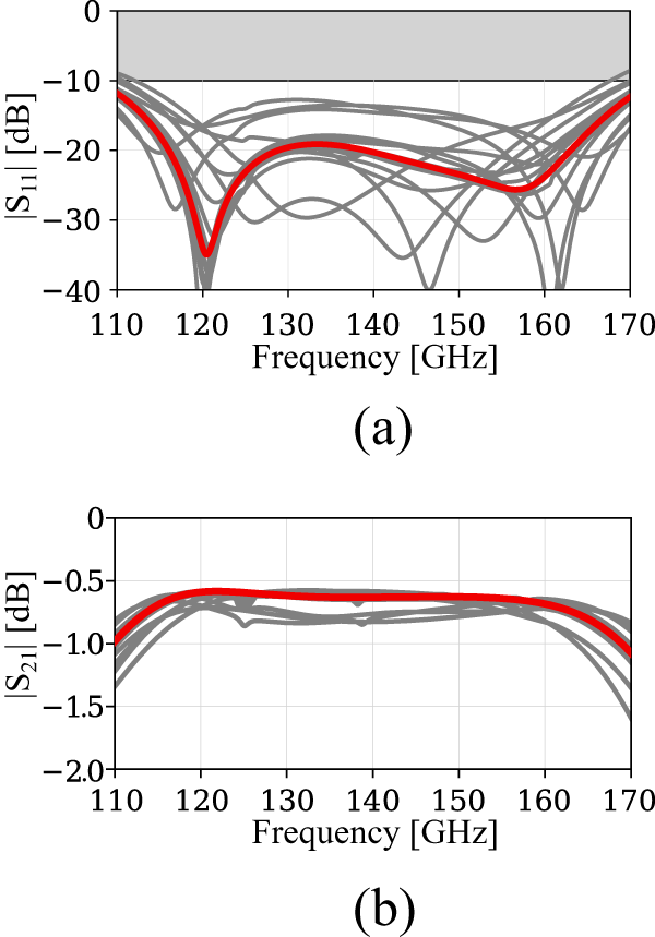
To further assess the robustness of the superstrate-based design with respect to fabrication tolerances in the remaining design parameters, Fig. 8(a) and 8(b) present a cornerstone analysis alongside the nominal reflection coefficient and insertion loss. The results confirm that the design maintains robust full D-band coverage, achieving a nominal FBW of 46 % with a simulated insertion loss of 0.65 dB. Based on manufacturer data [27], variations of up to 50  $\unicode{x03BC}$m in the slot, patch, and cavity dimensions, as well as 10 % deviations in each substrate height, have been considered. The transition is found to be resilient to variations of this scale. The largest deviations in behavior are found to be caused by the slot length
 $\text{L}_\text{s}$ and patch length
 $\text{L}_\text{p}$, which control the resonances of the design. Particularly, a decrease in
 $\text{L}_\text{p}$ exceeding 50
 $\unicode{x03BC}$m is most critical, as it may occur due to overetching and leads to mismatch within the D-band. Meanwhile, slot length variations of up to 75
 $\unicode{x03BC}$m can be tolerated. Moreover, the simulations show that the structure exhibits linear phase behavior within the entire -10 dB impedance bandwidth.
Nominal reflection coefficient (a) and insertion loss (b) of the superstrate-based transition subject to variations of up to 50  $\unicode{x03BC}$m in slot, patch and cavity dimensions, as well as 10 % variations in each substrate height, indicating full D-band coverage with low insertion loss under all expected parameter variations.

Figure 8 Long description
A line graph with the y-axis labeled, vertical bar S11 vertical bar, in decibel, ranging from minus 40 to 0 with ticks at minus 40, minus 30, minus 20, minus 10 and 0. The x-axis is labeled Frequency, in gigahertz, ranging from 110 to 170 with ticks at 110, 120, 130, 140, 150, 160 and 170. Multiple curves are plotted, including one thicker curve. The thicker curve is near minus 12 decibel at 110 gigahertz, drops to about minus 35 decibel near 120 gigahertz, rises to about minus 20 decibel near 130 gigahertz, stays around minus 20 to minus 25 decibel from about 130 to 160 gigahertz, then rises to about minus 12 decibel at 170 gigahertz. The image B showing a line graph with the y-axis labeled, vertical bar S21 vertical bar, in decibel, ranging from minus 2.0 to 0 with ticks at minus 2.0, minus 1.5, minus 1.0, minus 0.5 and 0. The x-axis is labeled Frequency, in gigahertz, ranging from 110 to 170 with ticks at 110, 120, 130, 140, 150, 160 and 170. Multiple curves are plotted, including one thicker curve. The thicker curve is about minus 1.0 decibel at 110 gigahertz, rises to about minus 0.6 decibel near 120 gigahertz, stays near minus 0.6 to minus 0.7 decibel from about 120 to 160 gigahertz, then drops to about minus 1.0 decibel at 170 gigahertz.
Experimental validation
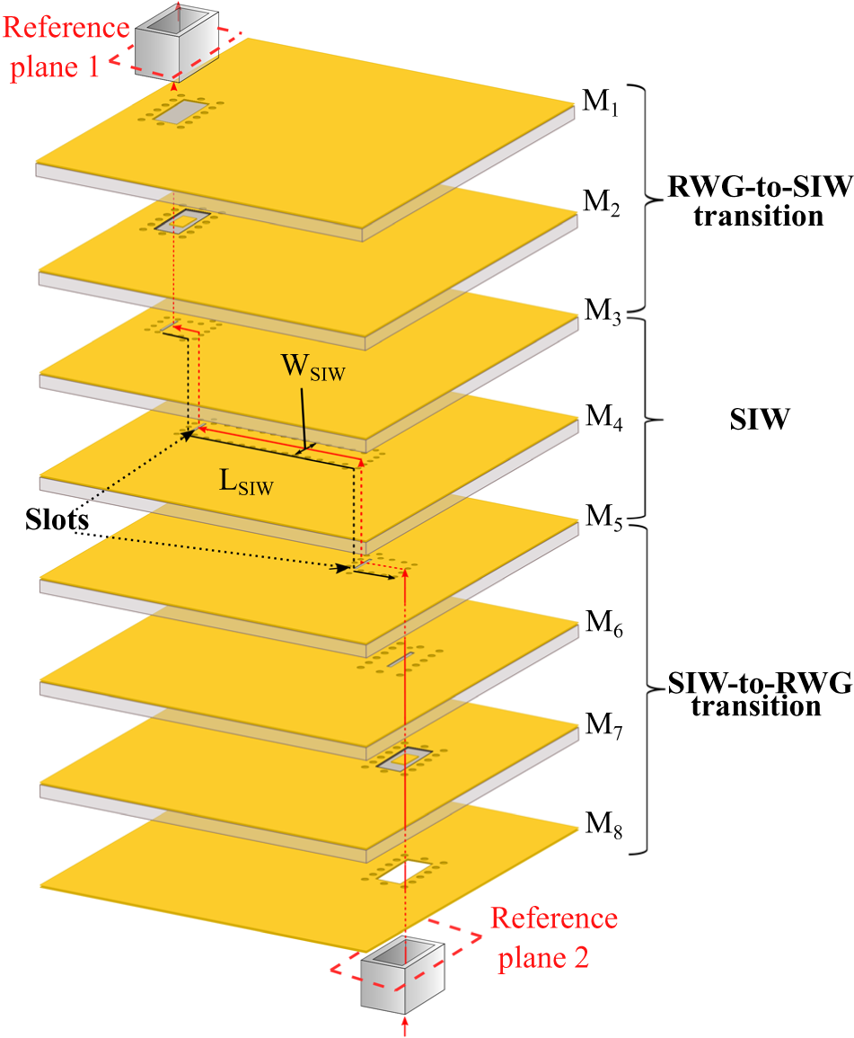
To validate its performance, a back-to-back configuration of the superstrate-based RWG-to-SIW transition component is manufactured using a standard HDI PCB fabrication process. To accommodate the range-extender waveguide flanges, an SIW section of at least 11 mm in length ( $\text{L}_{\text{SIW}}$) is required between the two transitions. To keep this length as short as possible, the transitions are placed on opposite sides of the PCB within the resulting eight-layer stack-up. Additional slot-coupled SIW layer transitions are introduced in metal layers
 $\text{M}_4$ and
 $\text{M}_5$ to connect the two transitions with minimal influence on the overall back-to-back behavior (Fig. 9). To estimate the extra insertion loss contributed by the SIW sections, prototypes with different SIW lengths (
 $\text{L}{\text{SIW}}$ = 11.35 mm and 13.75 mm) are included on the fabricated panels, enabling the extraction of the line-length-dependent losses from the measurement data [Reference Declercq, Rogier and Hertleer28].
Back-to-back RWG-to-SIW transition connected by an SIW section of length  $\text{L}_\text{SIW}$.

Figure 9 Long description
An eight-layer printed circuit board stack-up. At the top, labeled M1 and M2, is the RWG-to-SIW transition. Below, layers M3 to M5 form the SIW section, with slots indicated between M4 and M5. The width of the SIW is marked as W subscript SIW and the length as L subscript SIW. The bottom layers, M6 to M8, show the SIW-to-RWG transition. Reference plane 1 is at the top and reference plane 2 is at the bottom, with dashed lines connecting them vertically through the layers.
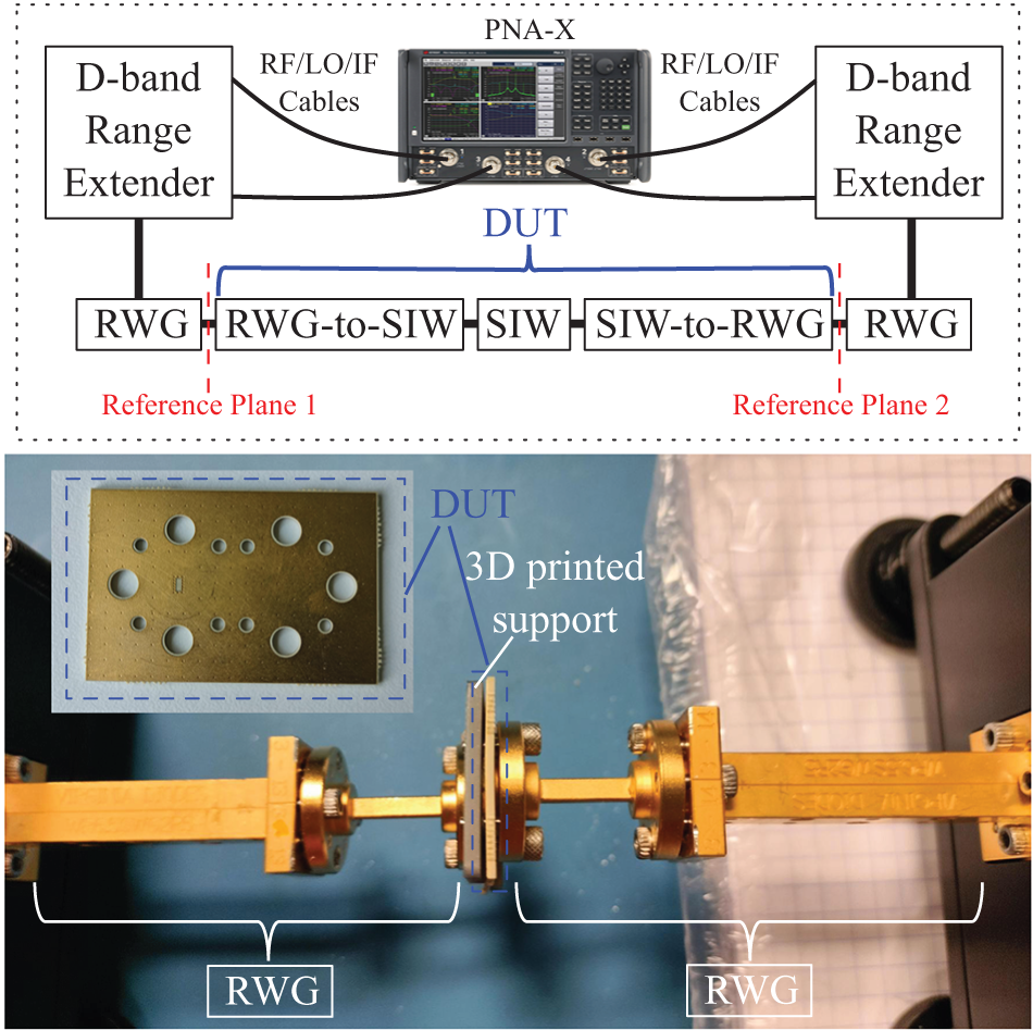
The S-parameters are measured with a Keysight N5242B PNA-X microwave network analyzer in combination with Virginia Diode Incorporated (VDI) D-band VNA extenders [29] and WR-6 RWGs. The measurement setup, including the locations of the thru–reflect–line (TRL) calibration reference planes, is shown in Fig. 10. During the measurements, 3D-printed structures are used as supports to clamp the RWG and PCB together, ensuring alignment and air-gap-free contact. The proposed setup and TRL calibration allow for measurements of four prototypes from two successfully manufactured panels to be measured at the PCB interface, allowing for direct comparison to simulation.
Measurement setup of the back-to-back RWG-to-SIW transition using Virginia Diode Incorporated (VDI)’s D-band range extenders.

Figure 10 Long description
The image consists of two parts. The top part is a schematic diagram illustrating the measurement setup for the back-to-back RWG-to-SIW transition. It includes D-band range extenders connected to a PNA-X microwave network analyzer via RF/LO/IF cables. The device under test, labeled as DUT, is positioned between two reference planes, marked as Reference Plane 1 and Reference Plane 2. The DUT consists of components labeled RWG, RWG-to-SIW, SIW, SIW-to-RWG and RWG, connected in sequence. The bottom part of the image shows a photograph of the physical setup. It features a close-up view of the DUT supported by 3D printed structures, ensuring alignment and contact between the RWG and PCB. The RWG components are visible on either side of the DUT, with the 3D printed support clearly labeled. An inset in the photograph highlights the DUT with visible holes and structural details.
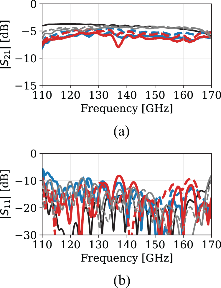
Fig. 11 shows the measured S-parameters of the entire back-to-back transition structure for two different line lengths, indicating that the back-to-back reflection coefficients align well with simulation across the entire D-band. All four measured prototypes exhibit good matching throughout the band. The average insertion losses of the 11.35 mm and 13.75 mm SIW lines equal 5.2 dB and 6 dB, respectively, which corresponds to a measured SIW loss of 0.33 dB/mm in the Megtron 7 substrate, compared to 0.28 dB/mm in simulation. From these results, the average single-ended transition insertion loss is determined to be 0.95 dB, slightly higher than the simulated value of 0.65 dB. This difference is attributed to increased substrate, conductor, and surface-roughness losses, consistent with the marginally higher measured SIW loss. Additional simulations indicate that the observed excess loss can be reproduced either by assuming a surface roughness of approximately 2  $\unicode{x03BC}$m or by increasing the dielectric loss tangent to 0.0125, providing representative upper-bound estimates for these parameters. In practice, the measured loss is expected to result from a combination of both effects. The average in-band variation of the insertion loss is 0.15 dB.
Transmission coefficient (a) and reflection coefficient (b) of the back-to-back transitions of the equivalent circuit (black), EM-simulated (gray), panel 1 (blue), and panel 2 (red) results. The 11.35-mm-long-line is indicated by the dashed lines, and the 13.75-mm-long line with full lines.

Figure 11 Long description
A line graph with the y-axis labeled, S21, in decibel, ranging from 0 to minus 15. The x-axis is labeled, Frequency, in gigahertz, ranging from 110 to 170 with ticks at 110, 120, 130, 140, 150, 160 and 170. Multiple solid and dashed curves are plotted. At 110 gigahertz, curves lie between about minus 8 and minus 4 decibel. From 120 to 170 gigahertz, most curves stay between about minus 7 and minus 4 decibel. One curve shows a pronounced dip near about 138 gigahertz reaching about minus 8 decibel, then returns to around minus 6 to minus 5 decibel. The image B showing a line graph with the y-axis labeled, S11, in decibel, ranging from 0 to minus 30. The x-axis is labeled, Frequency, in gigahertz, ranging from 110 to 170 with ticks at 110, 120, 130, 140, 150, 160 and 170. Multiple solid and dashed curves are plotted with repeated peaks and notches across the band. Values span roughly from about minus 8 to near minus 30 decibel. Several curves reach notches close to minus 30 decibel around the mid band, including near about 140 gigahertz and near about 150 to 155 gigahertz. Around 160 to 170 gigahertz, curves continue oscillating, with some rising toward about minus 10 decibel and others remaining below about minus 20 decibel.
Conclusion
A novel broadband RWG-to-SIW transition has been presented that achieves a 46 % bandwidth for  $|S_{11}| \lt -10$ dB, enabling full coverage of the 110–170 GHz D-band. This performance is realized by co-optimizing a resonant slot and an aperture-coupled patch together with a dielectric-loading superstrate. In this contribution, an equivalent circuit model was introduced to analyze the transition’s underlying operating mechanisms more thoroughly and to provide practical guidelines for selecting the optimal slot and patch resonance frequencies as well as the optimal superstrate height. Additionally, the superstrate is proven to significantly improve the robustness of the presented component against fabrication tolerances, which are a primary concern at operating frequencies beyond 100 GHz. Comprehensive cornerstone analyses demonstrate that the proposed topology maintains stable performance across the full range of expected HDI PCB tolerances. Measurements performed on multiple fabricated prototypes exhibit good agreement with simulations, with a single-ended insertion loss below 0.95
 $\pm$ 0.15 dB, while preserving complete D-band coverage.
Overall, the proposed superstrate-based transition achieves wider bandwidth, lower insertion loss, and substantially greater robustness to manufacturing variations than competing approaches reported in the literature. These features make the proposed topology a highly attractive solution for reliable RWG-to-PCB interfacing in next-generation high-frequency communication and sensing systems.
Competing interests
The authors declare none.

Samuel Rimbaut received the M.Sc. degree in electrical engineering from Ghent University, Ghent, Belgium, in 2021, where he is currently pursuing the Ph.D. degree in electrical engineering with IDLab, Electromagnetics Group, Department of Information Technology (INTEC), IMEC. His research interests include next-generation communication systems, more specifically, highly efficient millimeter-wave and THz passive and active solutions. He received the Best Student Paper Award at the IEEE Electrical Design of Advanced Packaging and Systems Symposium (EDAPS) in 2025.

Kamil Yavuz Kapusuz received the M.Sc. degree in Electrical Engineering from Atilim University, Ankara, Turkey, in 2013, and the Ph.D. degree in Electrical Engineering from the Electromagnetics Group, Department of Information Technology, Ghent University, Belgium. From 2014 to 2016, he was a Senior Antenna Engineer at Remote Sensing Technologies, Turkey. From 2021 to 2022, he was a Visiting Scientist at CNRS, IETR Laboratory, France. Since 2022, he has been a Senior Researcher in Electromagnetics at IMEC and Ghent University. His research interests include the analysis and design of quasi-optical systems, leaky-wave antennas, near-field focusing techniques, in/on-body communication, millimeter-wave and sub-terahertz phased arrays, and EM modeling and optimization of 2.5D/3D RF packaging architectures. Dr. Kapusuz received the URSI Young Scientist Award at the 2021 URSI General Assembly. He was a co-recipient of the Best Student Paper on Antennas and Propagation Award at the EuCNC/6G Summit in 2024.

Sam Lemey received the M.Sc. degree in electronic engineering from Howest, University College West Flanders, Kortrijk, Belgium, in 2012, and the Ph.D. degree in electrical engineering from Ghent University, Ghent, Belgium, in 2016. From January to March 2018, he was a Visiting Scientist with the Terahertz Photonics Group, IEMN, University of Lille Nord de France, Lille, France. He is currently a Professor with the Department of Information Technology, Ghent University, and a Guest Professor with IMEC. He has authored over 100 peer-reviewed journal and conference publications, with a Google Scholar H-index of 25 and over 2000 citations. His research interests include wearable and conformal antennas, active and optoelectronic antenna architectures for IoT and 5G/6G, millimeter-wave and sub-terahertz multi-antenna systems, ultra-wideband antennas for joint communication and sensing, and full-wave/circuit co-optimization. He received the 2020 URSI Young Scientist Award and multiple IEEE, ECOC, and Journal of Microwaves Best Paper Awards.

Hendrik Rogier received the M.Sc. and Ph.D. degrees in electrical engineering from Ghent University, Ghent, Belgium, in 1994 and 1999, respectively. From 2003 to 2004, he was a Visiting Scientist with the Mobile Communications Group, Vienna University of Technology, Vienna, Austria. He is currently a Senior Full Professor with the Department of Information Technology, Ghent University, and a Guest Professor with the Interuniversity Microelectronics Centre, Ghent. He authored or co-authored over 215 journal articles and over 250 conference papers. His research interests include antenna systems, radio wave propagation, body-centric communication, numerical electromagnetics, electromagnetic compatibility, and power/signal integrity. He is a member of MTT TC-26 RFID, Wireless Sensor and IoT Committee and AP-S TC-11 Health and Medicine, and serves as the URSI Commission B Representative for Belgium. He was an Associate Editor of IEEE Transactions on Microwave Theory and Techniques (2017–2019) and is currently an Associate Editor of two IET journals.










 Open access

