Introduction
The rapid growth of wireless sensor networks and the Internet of Things (IoT) has created a strong demand for reliable and long-term energy solutions for distributed low-power devices. Conventional batteries suffer from limited lifetime, periodic replacement requirements, and environmental and logistical constraints, particularly in remote or inaccessible locations [Reference Gorlatova, Sarik, Grebla, Cong, Kymissis and Zussman1]. To overcome these limitations, energy harvesting techniques exploiting ambient sources such as light, heat, vibration, and radio-frequency (RF) signals have emerged as promising solutions for enabling energy-autonomous systems [Reference Shinohara2]. In parallel, wireless power transfer (WPT) allows energy delivery over distance without physical connections, further supporting sustainable device operation [Reference Lu, Wang, Niyato, Kim and Han3].
With the global deployment of fifth-generation (5G) wireless networks, particularly in the sub-6 GHz bands, new opportunities have arisen for RF energy harvesting (RFEH) and far-field WPT [Reference Kishk and Alouini4]. Owing to their widespread availability, relatively stable power levels, and favorable propagation characteristics, sub-6 GHz 5G signals constitute an attractive ambient energy source for low-power electronic devices [Reference Moloudian, Hosseinifard, Kumar, Simorangkir, Buckley, Song, Fantoni and O’Flynn5, Reference Palattella, Dohler, Grieco, Rizzo, Torsner, Engel and Ladid6]. Moreover, research efforts are now extending beyond 5G toward millimeter-wave and terahertz bands, which promise higher available power density and wider bandwidths for energy harvesting applications [Reference Tran, Quan, Van Chien, Minh, Nguyen and Voznak7, Reference Pervez and Haider8]. These advancements align with the vision of next-generation IoT networks, where ubiquitous connectivity and self-powered nodes are key enablers of smart environments.
A key component in both RFEH and WPT systems is the rectenna, which combines an antenna for RF energy capture with a rectifier circuit that converts the received RF signal into usable DC power [Reference Lu, Wang, Niyato, Kim and Han3]. The overall system efficiency is largely determined by the RF-to-DC rectifier, particularly at low input power levels where diode nonlinearity and impedance mismatch significantly degrade performance [Reference Song, Huang, Zhou, Zhang, Yuan and Carter9]. Recent advances in antenna design, such as circularly polarized dielectric resonator antennas (DRAs), have further improved RFEH efficiency by offering polarization diversity and robustness in dynamic environments. For instance, a recent work [Reference Illahi, Iqbal, Ramay and Sulaiman10] introduced a circularly polarized MIMO wearable DRA addressing mutual coupling and integration challenges, providing valuable insights for compact and efficient rectenna design.
However, practical integration of rectennas into IoT and sensor networks remains challenging. Environmental variations, miniaturization constraints, and system-level integration with sensors and power management circuits introduce impedance mismatches and parasitic losses that limit RF-to-DC conversion efficiency [Reference Mushtaq, Venter, Singh and Owais11–Reference Psomas, Ntougias, Shanin, Xu, Mayer, Tran, Cottatellucci, Choi, Kim, Schober and Krikidis13]. These challenges motivate the development of rectifier architectures capable of maintaining high efficiency under variable RF input power conditions.
In practical scenarios, the received RF power depends on the transmitted power, operating frequency, antenna gains, and propagation distance, as described by the Friis transmission equation [Reference Friis14]. To maximize the harvested power, impedance matching between the antenna and the rectifier is essential, while low-pass filtering is typically employed to smooth the rectified DC output [Reference Wang, Ding, Hoang, Niyato, Wang and Dong In Kim15]. Nevertheless, the nonlinear behavior of Schottky diodes causes the rectifier input impedance to vary with frequency and input power, leading to significant efficiency degradation outside the design operating point [Reference Hagerty, Helmbrecht, McCalpin, Zane and Popovic16]. As a result, conventional rectifiers optimized for specific frequencies or power levels often exhibit limited performance under fluctuating RF conditions [Reference Wang, Ding, Hoang, Niyato, Wang and Dong In Kim15, Reference Costanzo and Masotti17].
Beyond antenna optimization, recent studies have increasingly focused on rectifier design and system-level solutions to improve RFEH performance. Adaptive impedance matching, dynamic load modulation, and hybrid rectifier architectures have been proposed to extend the operational input power range and enhance robustness in practical IoT systems [Reference Ali, Eid, Manaseer, AbuJaber and Ware18–Reference Helaly and Mohieldin21].
This work proposes a multi-range RF-to-DC rectifier approach operating at 3.5 GHz for WPT and RFEH applications. Three complementary rectifier architectures are designed and experimentally validated to efficiently cover low, high, and wide RF input power conditions. In particular, a passive dynamic sub-rectifier selection (DSRS) architecture is introduced to extend the operational input power range by dynamically directing the incident RF power toward the most suitable sub-rectifier through impedance adaptation only, without using switches or active control circuits. Compared to existing rectifiers, the proposed approach achieves an extended dynamic input power range while maintaining high conversion efficiency and low circuit complexity, making it well-suited for 5G-enabled IoT and energy-autonomous systems. The remainder of this paper is organized as follows. Section II reviews related work on RFEH rectifiers. Section III presents the rectifier architectures. Sections IV and V describe the low- and high-input-power rectifiers (HIPRs), respectively, including experimental validation and comparison with state-of-the-art designs. Section VI focuses on the wide-range rectifier based on the DSRS concept, and Section VII concludes the paper.
Rectifier architecture
The rectifier architecture, shown in Fig. 1, includes an input matching network, a high-frequency (HF) bandpass filter, a Schottky diode for RF-to-DC conversion, a low-pass filter for DC extraction, and a resistive load.
Typical RF-to-DC rectifier architecture.

Figure 1 Long description
The flowchart illustrates the RF-to-DC rectifier architecture. It begins with the 'Matching Network' connected by an arrow to the 'Input HF Filter.' This is followed by the 'Rectifying Unit (e.g., Diodes or MOS Transistors),' which connects to the 'Low-Pass Filter.' Finally, the 'Low-Pass Filter' leads to the 'Load Circuit.'.
The three proposed rectifier architectures target different RF input power regimes: a low-power rectifier optimized for weak RF signals, a high-power rectifier designed for strong RF excitation, and a wide-range rectifier based on a passive DSRS dual-path architecture enabling efficient operation over an extended input power range.
At sub-6 GHz 5G frequencies, microstrip RF-to-DC converter design must account for substrate and conductor losses, impedance matching accuracy, and parasitic effects, requiring compact layouts and accurate electromagnetic modeling to maintain high efficiency.
HF filter
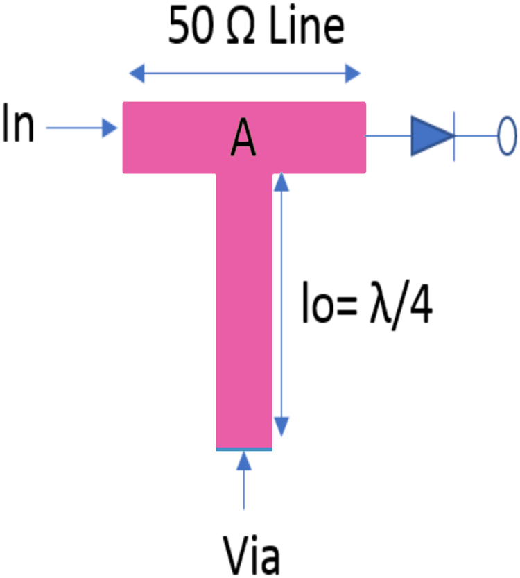
The HF filter in this rectifier design serves as a band-pass filter, strategically placed before the diode to attenuate harmonics generated during signal rectification from reflecting back toward the antenna, which could otherwise degrade system performance. As shown in Fig. 2, the filter is composed of a quarter-wavelength transmission line that is short-circuited to ground, creating a structure that selectively allows desired frequencies to pass while suppressing unwanted signals.
HF filter architecture.

Figure 2 Long description
The diagram shows a high-frequency filter architecture. It includes a 50 Ohm line labeled at the top, with an input marked 'In' on the left. The line connects to a T-shaped structure labeled 'A'. A diode is connected to the right of the T-structure, leading to an open circle. Below the T-structure, a vertical line labeled 'l subscript 0 equals lambda slash 4' extends downward to a point marked 'Via'.
DC filter
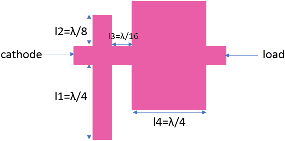
This element is designed to suppress the fundamental RF signal along with its harmonics, permitting only the rectified DC signal to reach the load. As illustrated in Fig. 3, the filter comprises four microstrip transmission lines (L1, L2, L3, L4) arranged to achieve the desired frequency-selective behavior. Each line is tailored to target specific unwanted frequency components while ensuring smooth DC output. L1 is a  $\lambda/4$ open-circuited line that behaves as a short-circuit at the fundamental frequency and its odd harmonics, effectively attenuating them. L2, designed as a
 $\lambda/8$ open-circuited line, is responsible for blocking the
 $2^nd$,
 $6^th$,
 $10^th$,
 $14^th$, and similar even-order harmonics, as determined by its resonance characteristics. L3, a
 $\lambda/16$ line, is specifically tuned to suppress the 4th harmonic. Lastly, L4 is a wide
 $\lambda/4$ line that functions as a parallel capacitor, effectively smoothing out the output voltage ripple and stabilizing the rectified DC component supplied to the load.
Typical RF-DC rectifier architecture.

Figure 3 Long description
A left-to-right layout shows a main horizontal conductor with the text “cathode” on the left side and the text “load” on the right side. From the main horizontal conductor, three vertical branches are shown on the left half. The leftmost branch goes downward and is labeled “L1=λ/4”. A second branch goes upward and is labeled “L2=λ/8”. A third branch goes upward and is labeled “L3=λ/16”. A wide rectangular section occupies the right half of the drawing and is connected to the main horizontal conductor. Along the bottom edge of this wide section, a downward branch is labeled “L4=λ/4”. No diode symbol, anode label, voltage label, current arrow, or component rating is shown.
Impedance matching network
In order to maximize the amount of power transferred to the diode, impedance matching is essential. In this context, several microstrip line matching techniques are employed.
• Impedance Matching Using a Single Transmission Line: In this approach, a single transmission line connects the antenna to the rectifying circuit whose impedance is characterized by a fixed power and load. The transmission line length
 $l$ and its characteristic impedance
$Z_l$ must be determined. For effective matching, the reflection coefficients must have equal magnitude:
\begin{equation*}
|\rho_{\text{ant}}| = |\rho_{\text{red}}|
\end{equation*}
Given:
(1)\begin{equation}
\rho_{\text{ant}} = \frac{Z_{\text{ant}} - Z_l}{Z_{\text{ant}} + Z_l}
\end{equation}(2)\begin{equation}
\rho_{\text{rect}} = \frac{Z_{\text{rect}} - Z_l}{Z_{\text{rect}} + Z_l}
\end{equation}where
$Z_{\text{ant}}$,
$Z_{\text{rect}}$, and
$Z_l$ are the antenna impedance, rectifier impedance, and line characteristic impedance, respectively. From these equations,
$Z_l$ can be determined. The line length
$l$ is given by:
(3)\begin{equation}
l = \frac{\lambda}{4\pi} \left( \arg(\rho_{\text{rect}}) - \arg(\rho_{\text{ant}}) \right)
\end{equation}This method offers advantages such as simplicity and compactness. However, it is only applicable when the resulting characteristic impedance
$Z_l$ is practical. For the line width to be manufacturable and to maintain a quasi-TEM mode,
$Z_l$ must satisfy the condition:
where
\begin{equation*}
Z_{\text{inf}} \lt Z_l \lt Z_{\text{sup}}
\end{equation*}
$Z_{\text{inf}}$ and
$Z_{\text{sup}}$ are the lower and upper practical limits, respectively.• Matching with Two Cascaded Transmission Lines: This method employs two consecutive transmission lines. The first transmission line with length
$l_1$ and characteristic impedance
$Z_1$, matches the rectifier impedance
$Z_{\text{rect}}$ to an intermediate impedance
$Z_A$, according to:
(4)\begin{equation}
Z_A = Z_1 \cdot \frac{Z_{\text{rect}} + jZ_1 \tan(\theta_1)}{Z_1 + jZ_{\text{rect}} \tan(\theta_1)}
\end{equation}A second line, with characteristic impedance
$Z_2$ and length
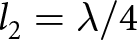
$l_2 = \lambda/4$, is then used to match
$Z_A$ to the antenna:
(5)\begin{equation}
Z_2 = \sqrt{Z_{\text{ant}} \cdot Z_A}
\end{equation}This technique may become impractical if
$Z_2$ falls outside the realizable range:
\begin{equation*}
Z_{\text{inf}} \lt Z_2 \lt Z_{\text{sup}}
\end{equation*}• Stub Matching
This technique involves inserting a stub with characteristic impedance
$Z_s$ in parallel at a distance
$d$ from the rectifier. The admittance of the stub is adjusted to compensate for the reactive component of the input impedance seen from the rectifier.This method is subject to fewer constraints, making it easier to implement.




Choice of the suitable Schottky diode
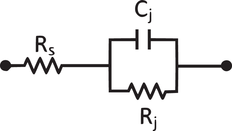
As a key component in RFEH circuits, the Schottky diode plays a critical role in determining the overall efficiency and performance of the rectifier. Its fast switching capability and low forward voltage drop make it particularly suitable for HF rectification. Consequently, careful diode selection is essential to ensure efficient RF-to-DC energy conversion. The electrical behavior of the Schottky diode is commonly represented using an equivalent circuit, as shown in Fig. 4, which provides insight into the diode operation and supports rectifier optimization.
Electrical modeling of the Schottky diode.

Figure 4 Long description
The diagram shows an equivalent circuit of a Schottky diode. It includes a series resistor labeled Rs connected to a parallel combination of a capacitor labeled Cj and a resistor labeled Rj. The series resistor Rs is connected to the left terminal and the parallel combination of Cj and Rj is connected between the series resistor and the right terminal. The capacitor Cj and resistor Rj are in parallel with each other, forming a branch that connects back to the main circuit path.
A Schottky diode is characterized by several key parameters, including the breakdown voltage ( $V_{br}$), series resistance (
 $R_s$), zero-bias junction capacitance (
 $C_{j0}$), and junction resistance (
 $R_j$), all of which significantly influence rectifier performance. The selection of a suitable diode is closely related to the expected RF input power level. In particular, the maximum power handling capability of the diode, given by (6), depends primarily on its breakdown voltage and the load resistance (
 $R_L$). Exceeding this limit may lead to diode breakdown and severe degradation of rectifier performance.
 \begin{equation}
P_{c}=\frac{V_{br}^2}{4R_{L}}
\end{equation}
The choice of Schottky diodes was driven by their low turn-on voltage, fast switching behavior, and suitability for microwave rectification. The SMS-7630 diode was selected for low-input-power operation due to its low barrier height and reduced junction capacitance, while the HSMS-2860 diode was chosen for high-input-power conditions because of its higher power handling capability. Other diode technologies were not considered, as they either require biasing networks or exhibit inferior performance at 3.5 GHz.
Low-input-power rectifiers (LIPRs) typically benefit from Schottky diodes with lower breakdown voltages and higher optimal load resistances, whereas HIPRs require diodes with higher breakdown voltages and lower load resistances to ensure reliable operation and high conversion efficiency.
Low-input-power rectifier
Geometrical description
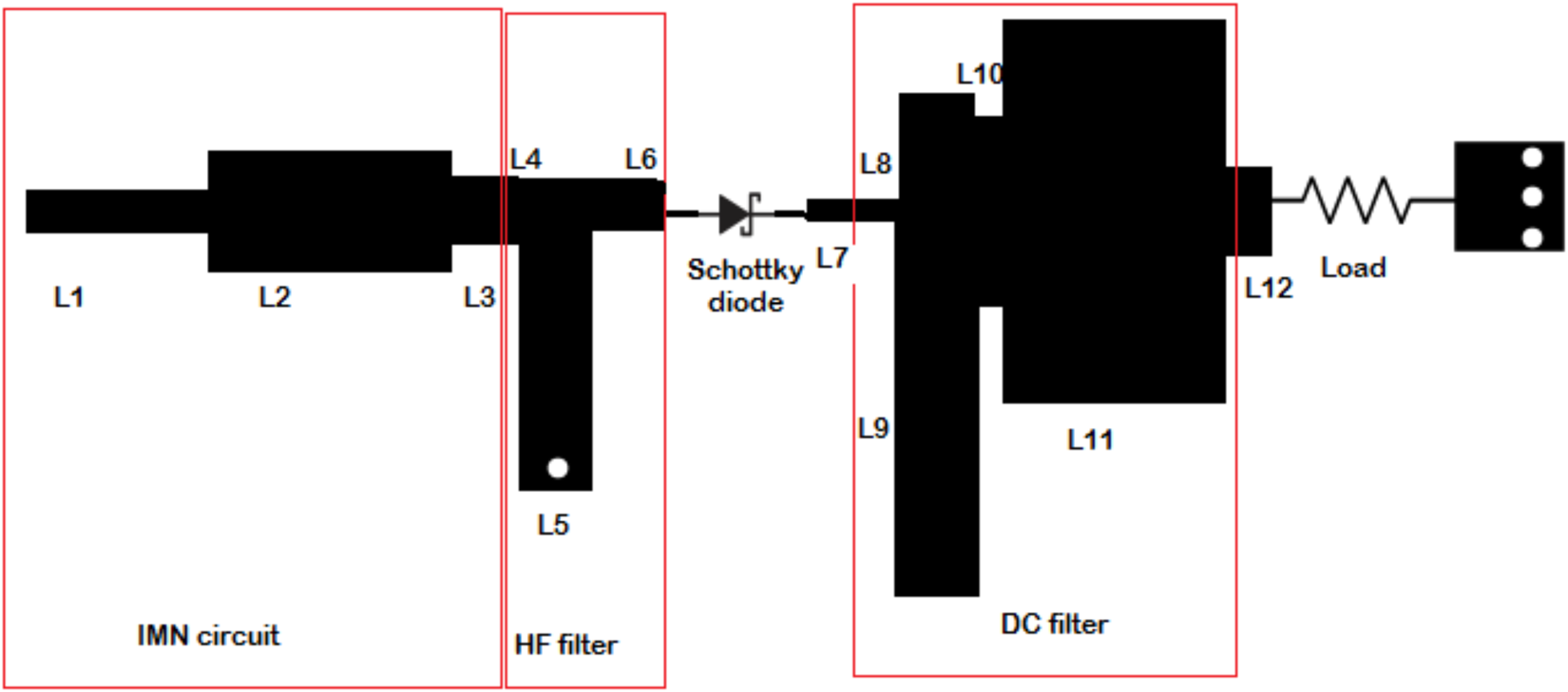
A simple series rectifier is proposed for RFEH in the sub-6 GHz 5G band, specifically at 3.5 GHz, as shown in Fig. 5. The rectifier is optimized for efficient operation under low RF input power levels (below 0 dBm). The circuit is fabricated on an FR4 substrate with a thickness of 1.6 mm, a relative dielectric constant of 4.4, and a loss tangent of 0.02.
Low-input-power rectifier design.

Figure 5 Long description
The diagram illustrates a series rectifier circuit with three main sections: an input matching network (IMN), a high-frequency (HF) filter and a DC filter. The IMN includes inductors labeled L1, L2 and L3, connected in series. The HF filter consists of inductors L4, L5 and L6, with L5 shunted to ground. A Schottky diode, labeled L7, follows the HF filter, oriented to allow current flow from left to right. The DC filter comprises inductors L8, L9, L10 and L11, with L9 shunted to ground. The load is connected to L12, which follows the DC filter. The circuit flows from left to right, starting at the IMN and ending at the load. Labels L1 to L12 indicate the sequence of components, with the Schottky diode performing rectification and the DC filter smoothing the output to direct current for the load. The layout is left-to-right, with input at the IMN and output at the load, ensuring clear signal flow and connectivity.
The simple series diode topology was chosen due to its ease of integration and higher conversion efficiency. Alternative architectures based on voltage multipliers or multi-stage topologies were not retained, as they generally introduce increased losses, larger circuit size, higher complexity, and reduced efficiency.
For the LIPR, the SMS-7630 Schottky diode manufactured by Skyworks is employed due to its suitability for low-power operation. This diode exhibits high sensitivity to weak RF signals owing to its low turn-on voltage of 0.34 V and a reverse breakdown voltage of 2 V. To further optimize the rectifier performance under low input power conditions, a high load resistance of 1400  $\Omega$ is selected.
To ensure optimal power flow from the antenna to the rectifier, a matching network based on transmission lines was developed and implemented. The input impedance of the rectifier was initially measured to be approximately  $ Z_{\text{in}} = 9.97 + j1.5\,\Omega $ at the operating frequency of 3.5 GHz. To transform this impedance to match the standard 50
 $\Omega$ source impedance, a compact matching network consisting of three consecutive microstrip transmission lines in series was implemented (L1, L2, L3).
The impedance transformation using a lossless transmission line of characteristic impedance  $ Z_0 $, electrical length
 $ \theta $, and terminated with a load
 $ Z_L $, is governed by the well-known transmission line equation:
 \begin{equation*}
Z_{\text{in}}(\theta) = Z_0 \cdot \frac{Z_L + j Z_0 \tan(\theta)}{Z_0 + j Z_L \tan(\theta)}
\end{equation*}
Each of the three transmission lines was selected to progressively rotate the impedance toward the central region of the Smith Chart. To evaluate the impedance matching performance of the proposed rectifier, Smith Charts were used to visualize the input reflection coefficient ( $S_{11}$) under two conditions; frequency sweep and input power variation. As shown in Fig. 6(a), the impedance is well-matched to 50
 $\Omega$ at 3.5 GHz, where the normalized impedance is approximately 1.085+j0.068. This confirms that the matching network ensures efficient energy transfer at 3.5 GHz. Figure 6(b) illustrates the impact of varying input power from -20 dBm to 0 dBm on the input impedance. Despite slight variations, the impedance remains close to the central region of the Smith Chart, demonstrating the stability and robustness of the matching network for low RF power.
(a)  $S_{11}$ on a Smith Chart vs. frequency. (b)
 $S_{11}$ on a Smith Chart vs. input power.

Figure 6 Long description
The image A showing a Smith chart plot of S(1,1) with a single red trace and one marker labeled m1. The sweep label reads RFFreq (3.000 to 4.000). Marker readout: RFFreq equals 3.000; S(1,1) equals 0.862 slash minus 16.983; impedance equals Z0 times (2.721 minus j5.352). The trace forms a loop around the chart and the marker indicates one point on that loop. The image B showing a Smith chart plot of S(1,1) with a single red trace and one marker labeled m1. The sweep label reads RFPin (-20.000 to 0.000). Marker readout: RFPin equals 0.000; S(1,1) equals 0.141 slash minus 24.606; impedance equals Z0 times (1.284 minus j0.154). The trace forms a small loop and the marker indicates one point on that loop.
The optimized dimensions (lengths and widths) of the transmission lines used in the rectifier design are summarized in Table 1.
Optimized dimensions of the transmission lines forming the proposed rectifier

Table 1 Long description
The table lists optimized physical dimensions (width and length, in millimeters) for 12 transmission-line sections labeled L1 through L12. Widths span from 1 mm (L1 and L7) up to 17 mm (L11), making L11 a clear outlier in width. Lengths range from 2.3 mm (L3) to 13 mm (L1 and L9), with several lines clustered near 3 mm (L4 at 3.0 mm, L10 at 3.2 mm, and L12 at 3.0 mm). The longest sections are L1 (1 mm wide) and L9 (3.8 mm wide), both 13 mm long, while L3 is the shortest at 2.3 mm with a width of 4.7 mm. Most widths fall between about 3 and 5 mm (e.g., L2 4.8 mm, L3 4.7 mm, L4 3.1 mm, L5 3.3 mm, L8 3.4 mm, L9 3.8 mm, L10 3.0 mm, L12 3.0 mm). These values are design parameters only; the table does not provide tolerances, substrate details, or performance metrics, so functional implications cannot be inferred from dimensions alone.
Simulation performances
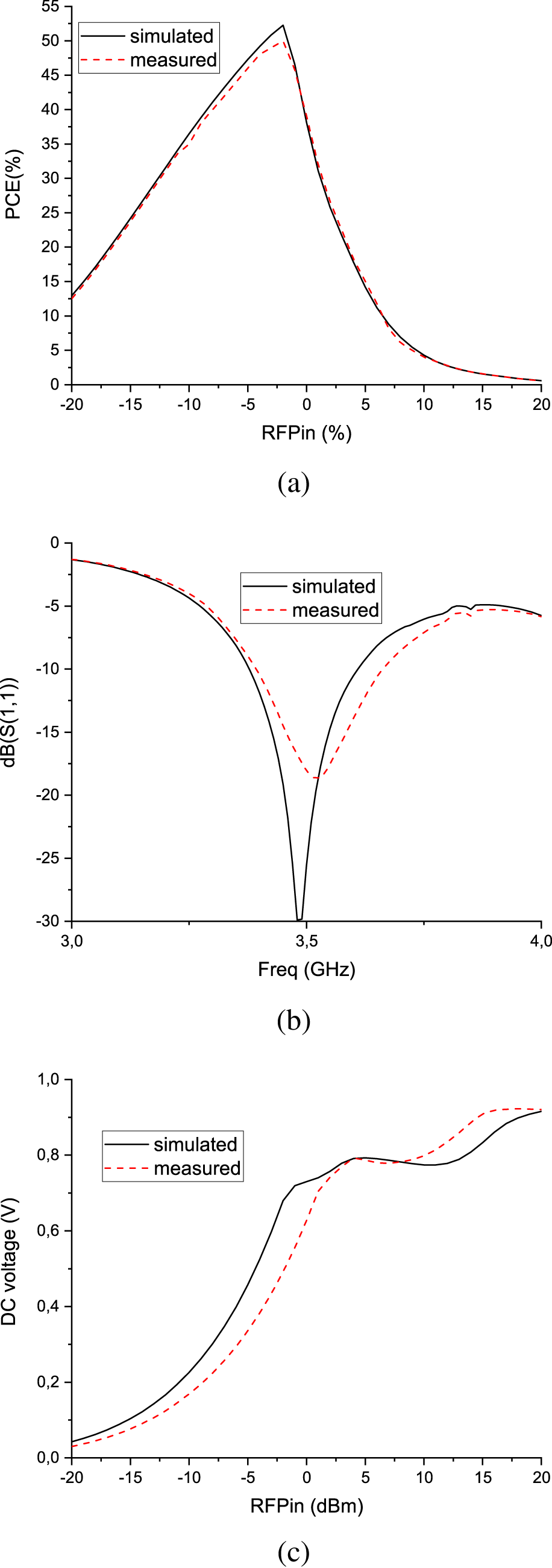
Performance assessment of the designed rectifier was performed via simulation tools at 3.5 GHz, focusing on the reflection coefficient, PCE, and the resulting DC voltage spanning multiple input power values. The simulation results, as depicted in Fig. 8 reveal that the rectifier exhibits good impedance matching at 3.5 GHz ( $S_{11}$
 $ \lt $-30 dB). Furthermore, it is evident that LIPR presents a peak efficiency of 52.2% at –2 dBm, accompanied by a DC output voltage of approximately 0.7 V. Moreover, the PCE remains consistently above 30% over a wide RF power range (from –13 to –1 dBm), highlighting the circuit’s suitability for low-power RFEH applications.
Experimental validation
To validate the performance of the proposed LIPR, experimental measurements were conducted at 3.5 GHz using a dedicated RF test setup.
The rectifier was directly connected to the measurement apparatus, and the reference plane for all measurements was defined at the SMA connector interface of the input port. No fixture de-embedding was applied. S-parameter measurements were performed using a Keysight FieldFox N9925A vector network analyzer calibrated at the SMA reference plane, while the RF input signal was generated using a Keysight N5171B RF signal generator.
The measured RF-to-DC conversion efficiency was calculated as the ratio between the DC output power and the RF input power set on the signal generator. The RF input power was swept from  $-20$ dBm to
 $+20$ dBm in 1 dB steps. At each input power level, the DC output voltage was recorded using a digital multimeter, and the corresponding DC power was computed as
 $P_{\mathrm{DC}} = V_{\mathrm{DC}}^{2}/R_{\mathrm{L}}$.
The prototype was fabricated on an FR4 substrate and experimentally evaluated under varying input power conditions, as shown in Fig. 7.
(a) LIPR prototype. (b) Measurement setup.

Figure 7 Long description
Image (a) shows the LIPR prototype mounted on a rectangular printed circuit board. A coaxial connector is positioned at the left edge of the board and connects to a copper trace structure that extends across the board surface. No discrete components are visibly present beyond the trace structure and connectors. A red wire and a black wire are attached at the right side of the board, forming the output terminals. Image (b) shows the measurement setup. The printed circuit board is placed on a surface. A coaxial cable connects the left side of the board to an instrument positioned to the left. The red and black output wires on the right side of the board are connected to the probe leads of a digital multimeter. The multimeter display reads 4.63 Volts. The red probe connects to the red output wire and the black probe connects to the black output wire, with the 4.63 Volts reading measured across these two output terminals.
The measured results depicted in Fig. 8 confirm the trends observed in simulations. A peak RF-to-DC conversion efficiency of 50.5% was achieved at an input power level of  $-2$ dBm, corresponding to a DC output voltage of 0.7 V.
Simulated and measured results of the LIPR: (a) RF-to-DC conversion efficiency, (b) input reflection coefficient  $S_{11}$, and (c) DC output voltage.

Figure 8 Long description
The image A showing a line graph with a legend listing simulated and measured. The horizontal axis label is RFPin (percent), ranging from negative 20 to 20. The vertical axis label is PCE(percent), ranging from 0 to 55. The simulated curve rises from about 13 at negative 20 to about 52 near negative 2, then drops to about 0 near 20. The measured curve follows a similar shape, rising from about 12 at negative 20 to about 50 near negative 2, then dropping to about 0 near 20. The image B showing a line graph with a legend listing simulated and measured. The horizontal axis label is Freq (gigahertz), ranging from 3.0 to 4.0. The vertical axis label is dB(S(1,1)), ranging from negative 30 to 0. The simulated curve decreases from about negative 1 at 3.0 to a minimum near negative 30 at about 3.5, then increases to about negative 6 near 4.0. The measured curve decreases from about negative 1 at 3.0 to a minimum near negative 19 at about 3.5, then increases to about negative 6 near 4.0. The image C showing a line graph with a legend listing simulated and measured. The horizontal axis label is RFPin (decibel milliwatt), ranging from negative 20 to 20. The vertical axis label is DC voltage (V), ranging from 0.0 to 1.0. The simulated curve increases from about 0.05 at negative 20 to about 0.7 near negative 2, reaches about 0.8 near 4, stays near 0.78 to 0.8 around 5 to 12, then increases to about 0.9 near 20. The measured curve increases from about 0.03 at negative 20 to about 0.7 near 0, reaches about 0.78 near 4, stays near 0.78 to 0.8 around 5 to 10, then increases to about 0.92 near 15 and remains near 0.92 to 0.93 near 20.
The measured results show close agreement with simulations in terms of peak efficiency and operating power range, validating the accuracy of the proposed design approach.
Minor discrepancies between simulated and measured results are mainly attributed to substrate losses, fabrication tolerances, including microstrip line dimension variations, diode parameter dispersion, fluctuations in substrate thickness and dielectric constant, as well as connector imperfections. Overall, the experimental validation confirms that the proposed rectifier operates reliably and efficiently, making it well-suited for low-power wireless energy harvesting and WPT applications targeting battery-free IoT devices and sensors.
Performance comparison and discussion
To evaluate the performance of the proposed LIPR, a comparison is conducted with representative state-of-the-art designs operating at a single frequency. Table 2 summarizes key performance metrics, including operating frequency, input power level, maximum power conversion efficiency (PCE), rectifying element, topology, and substrate. As summarized in Table 2, the proposed LIPR exhibits competitive conversion efficiency compared to state-of-the-art designs operating at similar frequencies. In particular, the proposed rectifier achieves a higher PCE at comparable or lower input power levels. This improvement is mainly attributed to the optimized series topology and the use of the SMS-7630 Schottky diode, which is well-suited for low-power rectification.
Performance comparison of state-of-the-art low-power rectifiers

Table 2 Long description
The table compares low-power RF rectifiers by operating frequency (GHz), maximum power conversion efficiency (PCEmax) with the input power level where it occurs (dBm), rectifying element, topology, and substrate. “This work” reports the best efficiency: 50.5% PCEmax at −2 dBm at 3.5 GHz using an SMS-7630 diode in a series topology on FR4. Other 3.5 GHz designs using SMS-7630 reach 45% at −2 dBm (series on FR4) and 43.5% at 0 dBm (series doubler; substrate not specified). Lower-frequency examples show lower peak efficiencies: 20% at 2.45 GHz with an HSMS-2852 voltage doubler on FR4 at −20 dBm, and 20% at 0.915 GHz using two HSMS-2852 diodes in a 2-stage voltage multiplier on TLX8 at −5 dBm. Across entries, higher PCE values cluster at 3.5 GHz with SMS-7630-based series/series-doubler topologies. Comparisons should be interpreted cautiously because PCEmax is reported at different input power levels and one substrate entry is missing.
This comparison demonstrates that the proposed LIPR offers a favorable trade-off between conversion efficiency, input power sensitivity, and implementation simplicity at 3.5 GHz. The fully distributed microstrip-based design enables a compact layout and facilitates fabrication on low-cost FR4 substrates. These combined characteristics make the proposed rectifier a strong candidate for low-power RFEH applications, especially where size, cost, and integration constraints are critical.
High-input-power rectifier
Geometrical description
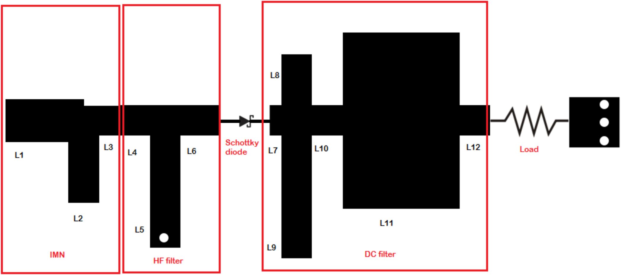
This rectifier (Fig. 9) is designed for WPT application. It employs the same substrate and structural configuration as used in LIPR. After evaluating the Schottky diode rectifier circuit based on the SMS-7630 for low-power systems, it becomes clear that this diode is unsuitable for high-power applications. Therefore, we propose using the HSMS-2860 diode instead. The datasheet of the HSMS-2860 diode indicates a high series resistance of 20  $\Omega$, and a low zero-bias junction capacitance of 0.18 p. Compared to other diodes, it offers better efficiency at high power levels at the operating frequency of 3.5 GHz. It is combined with a lower load resistance of 300
 $\Omega$ to ensure effective power handling and conversion efficiency at higher input power levels. Therefore, it is well-suited for high-power WPT applications.
High-input-power rectifier design.

Figure 9 Long description
The circuit diagram includes an input matching network (IMN) with components labeled L1, L2, L3 and L4. Following the IMN is a high-frequency (HF) filter with components L5 and L6. A Schottky diode is connected after the HF filter. The DC filter section includes components L7, L8, L9, L10 and L11. The output is connected to a load through L12. The load is represented by a resistive element and a connector with three terminals. Each section is enclosed in a red box with labels indicating IMN, HF filter and DC filter.
Matching a rectifier is challenging due to the nonlinear behavior of the rectifying diode, which causes the overall circuit impedance to vary with the input power level. As a result, the output power no longer changes linearly with the input power. The maximum efficiency of a rectifier depends on both the incident power and the load, and is achieved at a specific operating point. The matching network was designed using the “Smith Chart.” The input impedance  $Z_{\text{in}}$ of the complete system (HF filter + diode + DC filter + load) was first determined. The matching circuit was then designed to transform the complex input impedance
 $Z_{\text{in}}=(11+j1.5)~\Omega$ to 50
 $\Omega$. The selected matching network consists of an open-circuited stub with a length of 6 mm and a width of 3 mm, placed at a distance of 10 mm from the HF filter.
Simulation performances
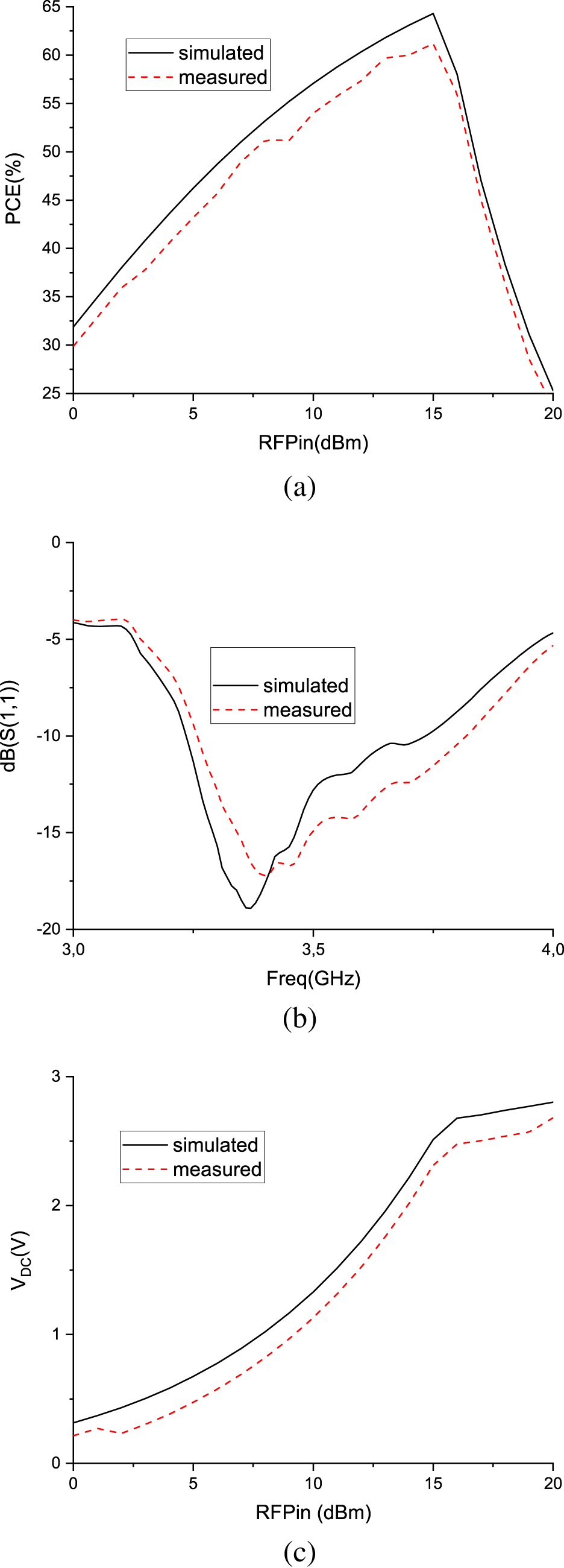
The simulation results shown in Fig. 10 confirm the effective performance of the rectifier at its operating frequency of 3.5 GHz under high input power conditions. The reflection coefficient  $S_{11}$ reaches a minimum of approximately
 $-19$ dB at 3.5 GHz, indicating excellent impedance matching between the antenna and the rectifier. This low reflection ensures that most of the incident RF power is transferred efficiently into the circuit with minimal loss. Regarding the RF-to-DC conversion, the rectifier achieves a peak efficiency of approximately 64% at an input power of 15 dBm. This high efficiency demonstrates the circuit’s ability to convert a significant portion of the RF energy into DC power when subjected to strong RF signals. Additionally, the output DC voltage increases progressively with the input power, reaching a maximum of about 2.9 V at 20 dBm. This voltage level is sufficient for powering low-power electronic components or charging energy storage elements in WPT systems. These results validate the suitability of the rectifier design for high-power energy harvesting at 3.5 GHz, with optimized impedance matching, high RF-to-DC efficiency, and appropriate DC output voltage.
Simulated and measured results of the HIPR: (a) RF-to-DC conversion efficiency, (b) input reflection coefficient  $S_{11}$, and (c) DC output voltage.

Figure 10 Long description
The image A showing a line graph with a legend listing simulated and measured. The horizontal axis label is RFPin(dBm), with a range from 0 to 20. The vertical axis label is PCE(percent), with a range from 25 to 65. Two curves are shown. The simulated curve rises from about 32 at 0 to about 64 at 15, then drops to about 25 at 20. The measured curve rises from about 30 at 0 to about 61 at 15, then drops to about 25 at 20. The label “(a)” appears below the plot. The image B showing a line graph with a legend listing simulated and measured. The horizontal axis label is Freq(GHz), with a range from 3.0 to 4.0. The vertical axis label is dB(S(1,1)), with a range from negative 20 to 0. Two curves are shown. The simulated curve is about negative 4 near 3.0, decreases to a minimum near about negative 19 around 3.35, then increases to about negative 5 near 4.0. The measured curve is about negative 4 near 3.0, decreases to a minimum near about negative 17 around 3.4, then increases to about negative 6 near 4.0. The label “(b)” appears below the plot. The image C showing a line graph with a legend listing simulated and measured. The horizontal axis label is RFPin (dBm), with a range from 0 to 20. The vertical axis label is Vdc(V), with a range from 0 to 3. Two curves are shown. The simulated curve increases from about 0.3 at 0 to about 2.7 at 15 and about 2.8 at 20. The measured curve increases from about 0.2 at 0 to about 2.5 at 15 and about 2.7 at 20. The label “(c)” appears below the plot.
Experimental validation
An experimental prototype of the rectifier was fabricated to validate the simulation results (Fig. 11(a)). The circuit was manufactured using standard microstrip technology on the same substrate as used in the simulation model. The Schottky diode HSMS-2860 was selected due to its favorable characteristics for high-input-power operation.
(a) HIPR prototype. (b) Measurement setup.

Figure 11 Long description
Image A shows a HIPR prototype circuit on a microstrip substrate with a Schottky diode and connected wires. Image B displays the measurement setup with the prototype connected to a multimeter showing a reading of 181.8 and a signal generator on the left side.
The output DC voltage was measured across a resistive load of  $300~\Omega$ using a digital multimeter. The measured reflection coefficient exhibits a minimum of approximately
 $-17$ dB at 3.5 GHz, which is in good agreement with the simulated result, confirming effective impedance matching in the fabricated prototype. In terms of power conversion performance, the maximum measured RF-to-DC efficiency reached 61.2% at an input power of 15 dBm, closely aligning with the simulated peak efficiency. The DC output voltage increases with input power, reaching 2.68 V at 20 dBm.
These results confirm the accuracy of the simulation model and the effectiveness of the proposed rectifier design for high-input-power scenarios at 3.5 GHz. The small differences observed between simulation and measurements can be mainly attributed to dielectric losses of the FR4 substrate, conductor losses in the microstrip lines, SMA connector losses, and parasitic effects of the Schottky diodes, which are not fully captured in simulation models. At 3.5 GHz, the relatively high loss tangent of FR4 limits the achievable peak efficiency. Future improvements could be achieved by employing low-loss substrates such as Rogers RO4350B or RO4003C, optimizing the layout to reduce parasitic inductances, and minimizing connector-related losses.
In this work, good agreement with simulations refers to the close correspondence between simulated and measured power conversion efficiency, DC output voltage, and operating input power range. The measured peak PCE values deviate from simulated results by only a few percentage points, while the overall efficiency trends versus input power are well preserved, confirming the validity of the proposed designs.
Performance comparison and discussion
To evaluate the performance of the proposed rectifier in high-power conditions, Table 3 presents a comparison with several recent high-power rectifier designs from the literature. Key parameters such as operating frequency, maximum PCE, rectifying elements, topology, and implementation details are highlighted. This comparison allows for a clear assessment of how the proposed design stands relative to other state-of-the-art solutions.
Performance comparison of state-of-the-art high-power rectifiers
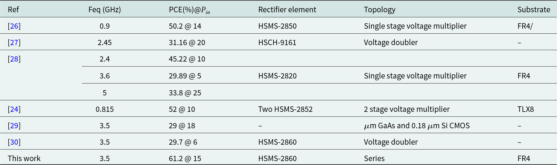
Table 3 Long description
The table compares high-power RF rectifiers by operating frequency (GHz), power-conversion efficiency (PCE) at a stated input power, rectifying element, circuit topology, and substrate. The best reported PCE is “This work” at 3.5 GHz: 61.2% PCE at input power 15, using an HSMS-2860 diode in a series topology on FR4. Other 3.5 GHz entries are notably lower: 29% at input 18 (rectifier element not specified; implemented in micrometer-scale GaAs and 0.18 micrometer Si CMOS), and 29.7% at input 6 using HSMS-2860 in a voltage-doubler topology (substrate not given). At lower frequencies, higher efficiencies than most prior 3.5 GHz designs are reported, including 52% at 0.815 GHz with two HSMS-2852 diodes in a 2-stage voltage multiplier on TLX8, and 50.2% at 0.9 GHz with HSMS-2850 in a single-stage voltage multiplier on FR4. Mid-band examples include 45.22% at 2.4 GHz (rectifier element/topology/substrate not listed) and 31.16% at 2.45 GHz using HSCH-9161 in a voltage doubler (substrate not listed). One reference lists multiple frequencies (3.6 GHz at 29.89% with HSMS-2820 on FR4, and 5 GHz at 33.8%) with some missing component and topology details. Comparisons should be interpreted cautiously because input power levels differ across rows and several cells are blank or marked with dashes, limiting like-for-like evaluation.
From the comparison study in Table 3, it can be clearly concluded that this rectifying circuit designed at 3.5 GHz offers several key advantages for energy transfer and harvesting applications, particularly within the 5G frequency band. Implemented using microstrip technology on a low-cost FR4 substrate, the circuit employs a simple single-diode series topology, which minimizes complexity, size, and component losses. The rectifier achieves a high peak efficiency of 61.2% at 15 dBm input power with a 300  $\Omega$ load and delivers a practical DC output voltage of 2.68 V, suitable for powering low-power electronics. These characteristics position the circuit as a cost-effective and high-performance solution for 5G-enabled WPT systems.
Wide input power range rectifier
This section introduces a wide input power range rectifier (WIPRR) based on a passive DSRS concept. Unlike most wide-dynamic-range rectifiers reported in the literature, which rely on active switches, power splitters, or reconfigurable biasing networks, the proposed architecture operates fully passively. The dynamic selection of the most suitable sub-rectifier is inherently achieved through impedance adaptation, enabling efficient RF-to-DC conversion over a wide range of input power levels while preserving a simple and compact circuit topology.
The DSRS dual-path architecture consists of two sub-rectifiers optimized for different RF input power levels and directly connected to the input port. Due to their distinct impedance behaviors, the sub-rectifier best matched to the incident RF power level is naturally activated, while the other remains weakly coupled. This passive self-selection mechanism enables efficient operation over a wide input power range without the need for RF switches, power splitters, or external control circuits.
Geometrical description
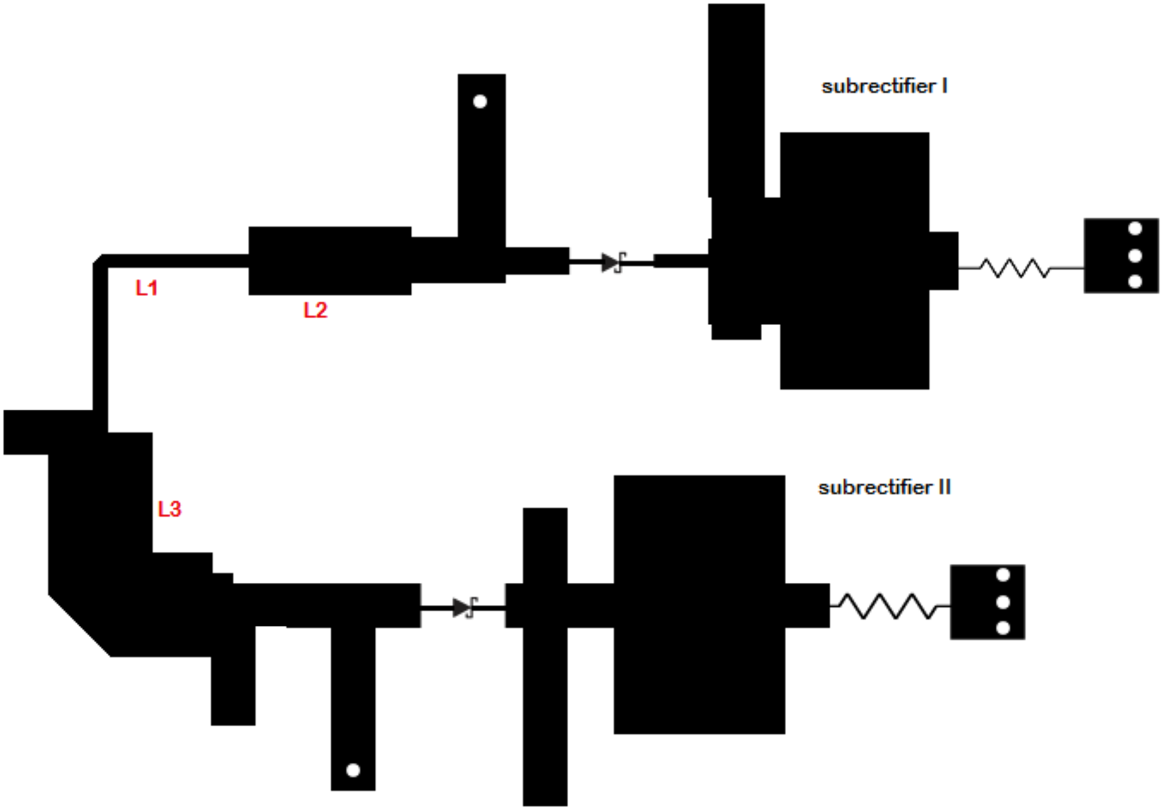
In this section, a rectifier designed to operate over a wide range of RF input power levels is presented (Fig. 12). The circuit is implemented using microstrip technology and consists of two parallel sub-rectifiers, labeled I and II, directly connected to the input port without any switching elements. Sub-rectifier I operates at 3.5 GHz and is optimized for low input power levels, while sub-rectifier II is designed to efficiently handle high input power conditions. Although both sub-rectifiers are based on architectures similar to those discussed in previous sections, their impedance matching networks (IMNs) have been specifically modified, and an additional matching network has been introduced to enable DSRS operation.
Wide input power range rectifier design.

Figure 12 Long description
The diagram shows a rectifier circuit with two parallel sub-rectifiers labeled I and II. Sub-rectifier I is connected to the input port through inductors labeled L1 and L2, followed by a diode. Sub-rectifier II is connected through inductor L3 and another diode. Both sub-rectifiers are connected to their respective loads. The circuit lacks any switching elements between the input port and the sub-rectifiers.
The IMN consists of three transmission lines, denoted as L1, L2, and L3. Transmission lines L1 and L2 are used to match sub-rectifier I to 50  $\Omega$ under low input power conditions, while presenting a high impedance at higher power levels. In contrast, transmission line L3 matches sub-rectifier II to 50
 $\Omega$ at high input power and presents a high impedance under low-power operation. The impedances
 $Z_{1}$,
 $Z_{2}$, and
 $Z_{3}$ represent the input impedances after each respective transmission line, while
 $Z_\mathrm{in}$,
 $Z_I$, and
 $Z_{II}$ denote the input impedances of the overall system, sub-rectifier I, and sub-rectifier II, respectively.
Using transmission line theory, the following equations are derived:
 \begin{equation}
Z_{2} = Z_{\mathrm{L2}} \cdot \frac{Z'_I + j Z_{\mathrm{L2}} \tan(\theta_{\mathrm{L2}})}{Z_{\mathrm{L2}} + j Z'_I \tan(\theta_{\mathrm{L2}})}
\end{equation}
 \begin{equation}
Z_{I} = Z_{\mathrm{L1}} \cdot \frac{Z_{2} + j Z_{\mathrm{L1}} \tan(\theta_{\mathrm{L1}})}{Z_{\mathrm{L1}} + j Z_{2} \tan(\theta_{\mathrm{L1}})}
\end{equation}
 \begin{equation}
Z_{II} = Z_{\mathrm{L3}} \cdot \frac{Z'_{II} + j Z_{\mathrm{L3}} \tan(\theta_{\mathrm{L3}})}{Z_{\mathrm{L3}} + j Z'_II \tan(\theta_{\mathrm{L3}})}
\end{equation}
The input power  $P_\mathrm{in}$ represents the total RF power delivered to the rectifier network, while
 $P_I$ and
 $P_{II}$ denote the power allocated to sub-rectifiers I and II, respectively. The DSRS consists of activating only one sub-rectifier depending on the input RF power level, and delivering the maximum available power (
 $P_\mathrm{in}$) to it, as illustrated in Fig. 13, which depicts the variation of input impedance for sub-rectifiers I and II as a function of input RF power.
Impedance variation of sub-rectifiers I and II versus input RF power.

Figure 13 Long description
Impedance The vertical axis is labeled Impedance. The horizontal axis is labeled Low Power, Input Power P subscript in, High Power. Two dashed curves are labeled Z subscript b and Z subscript a. Z subscript b slopes downward from the low power side toward the high power side. Z subscript a slopes upward from the low power side toward the high power side. The two curves cross near the middle of the plot, close to the label Input Power P subscript in. Text above the plot reads Sub-rectifier A active on the low power side and Sub-rectifier B active on the high power side.
At low power levels, the primary objective is to direct the maximum input power to the low-power sub-rectifier I. To achieve this, the input impedance  $Z_I$ must be matched to the source impedance
 $Z_G$, while the input impedance
 $Z_{II}$ must present a very high value. Conversely, at high power levels, the goal is to route the entire input power to sub-rectifier II. In this case,
 $Z_{II}$ must be matched to the source impedance, effectively deactivating sub-rectifier I, which now presents a high input impedance.
Simulation performances
The performance of the proposed WIPRR is evaluated in terms of input impedance ( $Z_\mathrm{in}$), reflection coefficient (
 $S_{11}$), and RF-to-DC conversion efficiency.
Input impedance
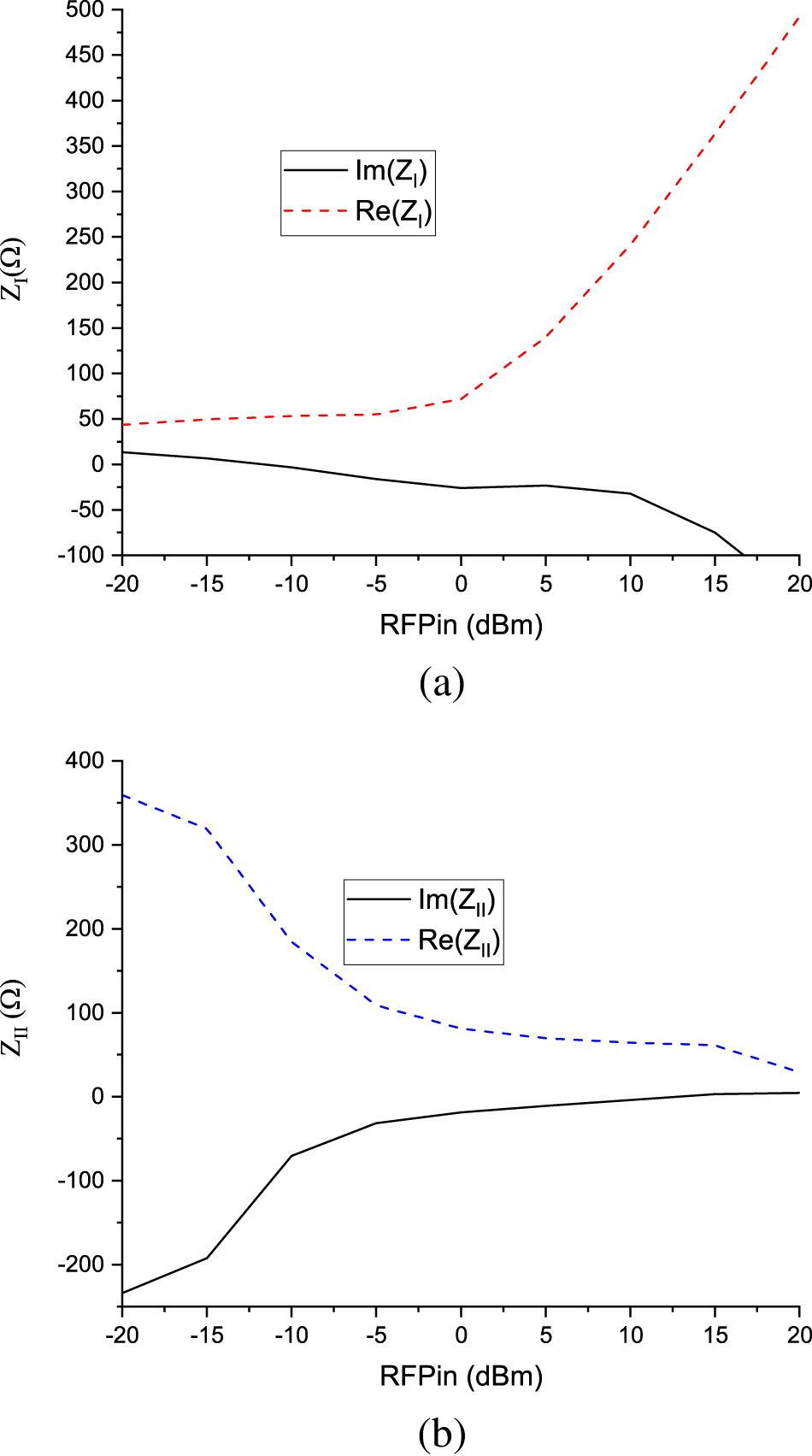
The input impedances as a function of the RF input power for sub-rectifiers I and II are shown in Fig. 14(a) and 14(b), respectively.
Simulation results of WIPRR. (a)  $Z_I$ vs
 $P_{in}$. (b)
 $Z_{II}$ vs
 $P_{in}$.

Figure 14 Long description
The image A showing a line graph with a legend listing Im(Z subscript I) and Re(Z subscript I). The horizontal axis is labeled RFPin (dBm), ranging from minus 20 to 20 with labeled ticks at minus 20, minus 15, minus 10, minus 5, 0, 5, 10, 15 and 20. The vertical axis is labeled Z subscript I (ohm), ranging from minus 100 to 500 with labeled ticks every 50. The Im(Z subscript I) curve starts near 10 at minus 20, is near 0 at minus 10, is near minus 20 at minus 5, is near minus 30 at 0, is near minus 25 at 5, is near minus 35 at 10, is near minus 80 at 15 and reaches minus 100 near 17. The Re(Z subscript I) curve is near 45 at minus 20, near 50 at minus 15, near 55 at minus 10, near 55 at minus 5, near 70 at 0, near 130 at 5, near 240 at 10, near 400 at 15 and near 500 at 20. The label (a) appears below the graph. The image B showing a line graph with a legend listing Im(Z subscript II) and Re(Z subscript II). The horizontal axis is labeled RFPin (dBm), ranging from minus 20 to 20 with labeled ticks at minus 20, minus 15, minus 10, minus 5, 0, 5, 10, 15 and 20. The vertical axis is labeled Z subscript II (ohm), ranging from minus 250 to 400 with labeled ticks at minus 200, minus 100, 0, 100, 200, 300 and 400. The Im(Z subscript II) curve is near minus 230 at minus 20, near minus 200 at minus 15, near minus 70 at minus 10, near minus 30 at minus 5, near minus 20 at 0, near minus 10 at 5, near minus 5 at 10, near 0 at 15 and near 5 at 20. The Re(Z subscript II) curve is near 360 at minus 20, near 320 at minus 15, near 180 at minus 10, near 110 at minus 5, near 80 at 0, near 70 at 5, near 65 at 10, near 60 at 15 and near 30 at 20. The label (b) appears below the graph.
Between -20 dBm and 0 dBm of RF input power, the input impedance  $Z_I$ remains approximately equal to 50
 $\Omega$; however, it behaves as a high impedance for
 $P_\mathrm{in} \gt 0$ dBm. Conversely, the input impedance
 $Z_{II}$ of sub-rectifier II is nearly 50
 $\Omega$ for
 $P_\mathrm{in}$ above 0 dBm, while it becomes very high for input power levels between -20 dBm and 0 dBm. These simulation results confirm that DSRS aligns with the behavior of the proposed rectifier. Depending on the RF power level, one sub-rectifier serves as the main energy harvester while the other is effectively deactivated.
Reflection coefficient
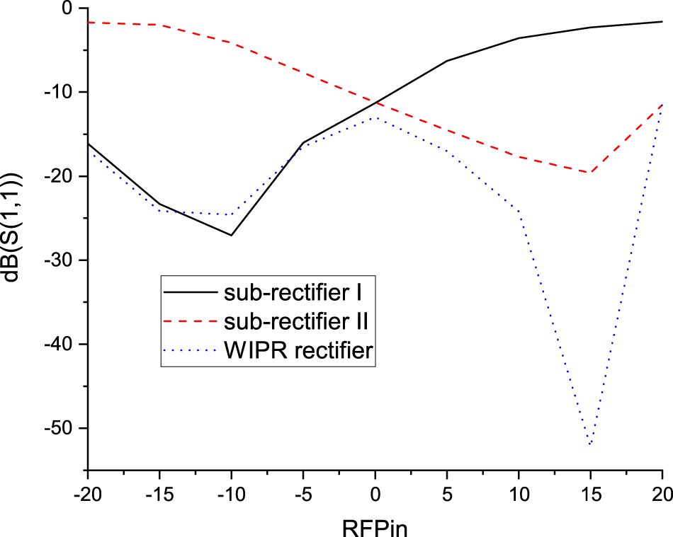
Figure 15 illustrates that sub-rectifier I is well matched for input power levels between -20 dBm and 0 dBm. Conversely, sub-rectifier II shows good matching for input powers above 0 dBm, where  $S_{11}$ consistently remains below -10 dB. Overall, the proposed WIPRR achieves good impedance matching across both low and high power levels.
Reflection coefficient  $S_{11}$ versus input RF power.

Figure 15 Long description
Reflection coefficient versus input RF power. Legend: sub-rectifier I; sub-rectifier II; WIPR rectifier. Vertical axis label: dB(S(1,1)). Range: 0 to minus 50. Horizontal axis label: RFPin. Range: minus 20 to 20. sub-rectifier I: (minus 20, minus 16), (minus 15, minus 23), (minus 10, minus 27), (minus 5, minus 16), (0, minus 12), (5, minus 6), (10, minus 3), (15, minus 2), (20, minus 1) sub-rectifier II: (minus 20, minus 2), (minus 15, minus 2), (minus 10, minus 4), (minus 5, minus 8), (0, minus 11), (5, minus 14), (10, minus 17), (15, minus 19), (20, minus 11) WIPR rectifier: (minus 20, minus 17), (minus 15, minus 24), (minus 10, minus 24), (minus 5, minus 17), (0, minus 13), (5, minus 17), (10, minus 24), (15, minus 52), (20, minus 12).
RF-to-DC conversion efficiency
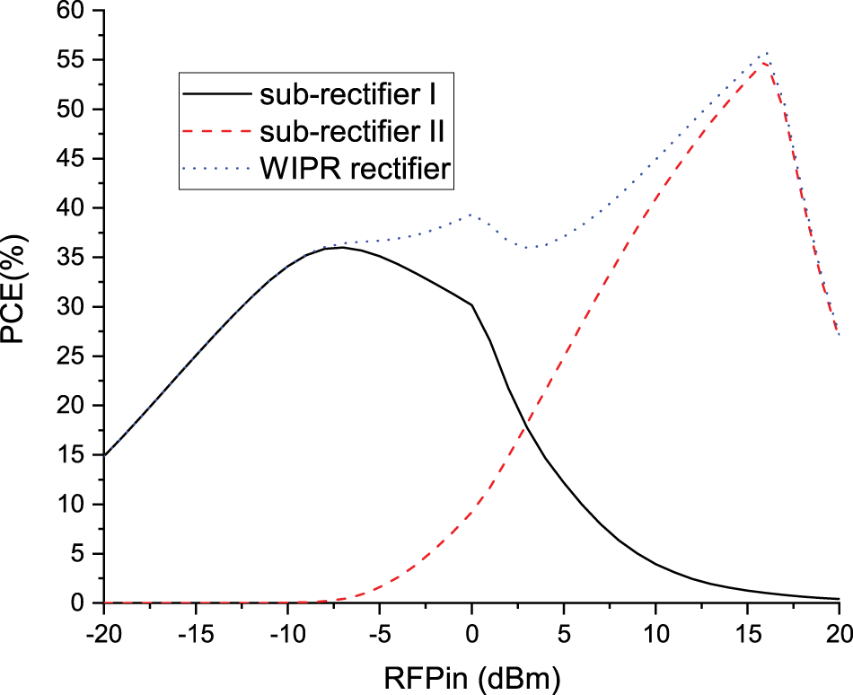
Figure 16 shows the RF-to-DC conversion efficiency as a function of the RF input power at 3.5 GHz. Sub-rectifiers I and II achieve peak efficiencies of 35% at -7 dBm, 40% at 0 dBm, and 56% at 16 dBm, respectively. The proposed WIPRR maintains an efficiency above 20% over a 38 dB range (from -16.5 dBm to 21.5 dBm), reaching 56% and 40% at 16 dBm and 0 dBm, respectively. In addition, the reflection coefficient remains below -10 dB across a 42 dB input power range.
RF-DC power conversion versus input RF power.

Figure 16 Long description
Legend: sub-rectifier I; sub-rectifier II; WIPR rectifier. Horizontal axis label: RFPin (dBm). Range: negative 20 to 20. Vertical axis label: PCE(percent). Range: 0 to 60. sub-rectifier I: (negative 20, 15), (negative 10, 35), (0, 30), (5, 12), (10, 4), (15, 1), (20, 0) sub-rectifier II: (negative 20, 0), (negative 10, 0), (0, 10), (5, 25), (10, 42), (15, 55), (20, 28) WIPR rectifier: (negative 10, 35), (negative 5, 37), (0, 39), (5, 36), (10, 45), (15, 56), (20, 28).
Experimental validation
The proposed WIPRR was fabricated using microstrip technology on a FR4 substrate. Precision connectors and ground vias were implemented to ensure accurate measurement and stable RF performance. The prototype (Fig. 18) was tested using VNA to measure the input reflection coefficient ( $S_{11}$), and a power source combined with a digital multimeter to evaluate the DC output voltage and compute the RF-to-DC conversion efficiency. All measurements were carried out at a frequency of 3.5 GHz.
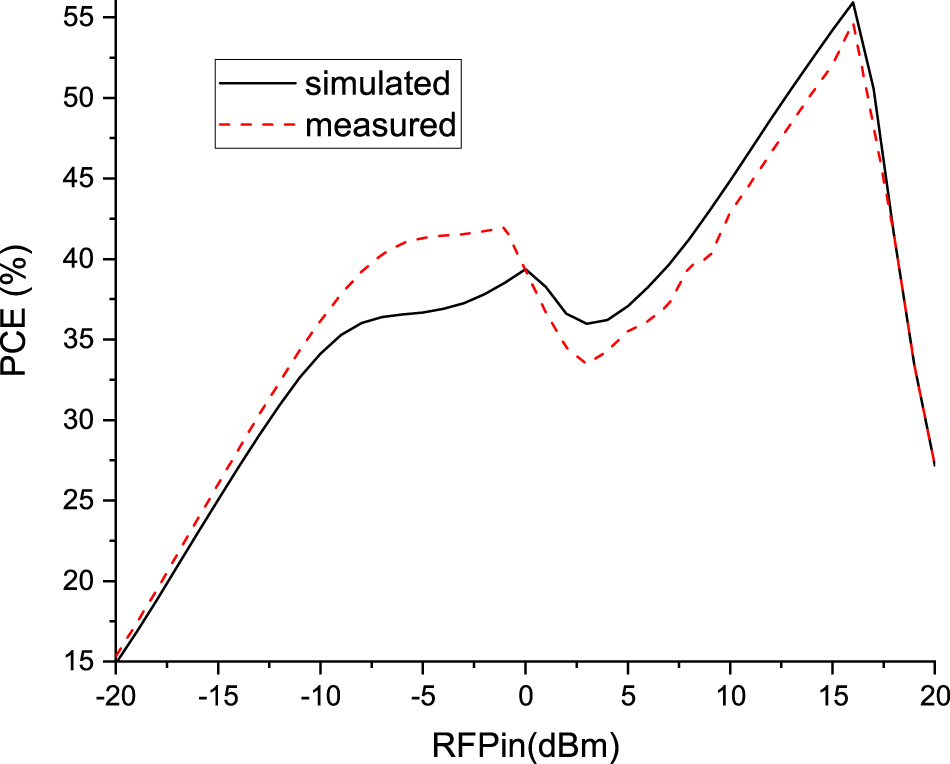
The experimental results are in good agreement with the simulation data, validating the design approach and the effectiveness of the DSRS technique. Figure 17 compares the simulated and measured RF-to-DC conversion efficiency across a wide range of input power levels at 3.5 GHz. The measured results closely follow the simulated curve, with minor discrepancies attributed to fabrication tolerances and measurement setup losses. The measured maximum PCE is 54.7% at 16 dBm, and it remains as high as 42% at -2 dBm. The rectifier exhibits an extended input power range of 41 dB (from -18 dBm to 23 dBm), over which the PCE consistently remains above 20%. The overall trend confirms the rectifier’s ability to maintain high efficiency over a broad input power range, validating the effectiveness of the proposed design.
Simulated and measured PCE of the proposed WIPRR at 3.5 GHz.

Figure 17 Long description
A line graph with a legend listing simulated and measured. Horizontal axis label: RFPin(dBm). Tick labels: negative 20, negative 15, negative 10, negative 5, 0, 5, 10, 15, 20. Vertical axis label: PCE (percent). Tick labels: 15, 20, 25, 30, 35, 40, 45, 50, 55. Legend entries and line styles: Simulated is a solid line. Measured is a dashed line. Plotted data values are shown as continuous lines without visible point markers. No coordinate pairs are explicitly labeled on the curves. Simulated (solid line) trace: Starts near (negative 20, 15). Rises to around the mid 30s by about negative 10. Continues upward to around 39 to 40 near 0. Drops to around 36 near 3. Rises to above 40 by about 10. Reaches a peak slightly above 55 near about 16. Drops sharply to the high 20s by about 20. Measured (dashed line) trace: Starts near (negative 20, 15). Rises to around 40 to 41 by about negative 6 to negative 5. Stays around 41 to 42 approaching 0. Drops to the mid 30s near about 3. Rises to around 40 by about 10. Reaches a peak slightly below the simulated peak near about 16. Drops sharply to the high 20s by about 20. Comparison between traces: Both traces rise from negative 20 to around negative 10, show a dip around 3, rise to a peak near about 16 and then drop sharply by 20. The measured dashed line is above the simulated solid line around negative 10 to 0 and below it around 10 to 16.
(a) WIPR prototype. (b) Measurement setup.

Figure 18 Long description
Image A shows a WIPR prototype on a brown substrate with microstrip technology. It includes precision connectors and ground vias, with red and black wires attached. Image B displays the same prototype connected to a digital multimeter, which shows a reading of 2.48. The setup includes various wires connected to the multimeter's ports, indicating a measurement process.
Performance comparison and discussion
As shown in Table 4, the proposed design achieves a peak RF-to-DC conversion efficiency of 54.7% at 16 dBm and maintains an efficiency above 20% over an exceptionally wide 41 dB input power range, from  $-18$ dBm to 23 dBm, at 3.5 GHz.
Performance comparison of state-of-the-art wide input power range rectifiers

Table 4 Long description
The table compares wide input power range rectifiers by operating frequency, peak power-conversion efficiency (PCE) at a stated input power, the technique used to extend dynamic range, and the input-power span where PCE stays above 20%. “This work” at 3.5 GHz reports the highest peak PCE, 54.7% at 16 dB input power, and the broadest >20% PCE band of 41 dB using a DSRS technique. Among prior references, the largest >20% PCE band is 25 dB for a 0.953 GHz dual-input design with 47.87% peak PCE at −19 dB input power. Other approaches include reconfigurable designs (0.820 and 0.902 GHz) with 39% and 33% peak PCE and 14 dB and 13 dB bands, resistance compression at 2.4 GHz with 47.1% peak PCE and a 16 dB band, and optimum voltage compensation at 0.896 GHz with 43% peak PCE but the narrowest band at 8.5 dB. Frequencies range from 0.820 to 3.5 GHz, and higher peak PCE does not consistently correspond to a wider >20% band across the referenced works. Because peak PCE is reported at different input power levels for each design, direct efficiency comparisons should be interpreted with that condition in mind.
Beyond peak efficiency values, a normalized comparison highlights the effectiveness of the proposed approach. When considering the trade-off between the achieved RF input power range and circuit complexity, the proposed DSRS-based rectifier offers a superior balance compared to previously reported designs summarized in Table 4. While several state-of-the-art rectifiers achieve high peak efficiency, their efficient operation is typically confined to a much narrower input power window. In contrast, the proposed rectifier maintains competitive efficiency over a significantly wider dynamic range at a comparable operating frequency, providing a more robust solution for practical RFEH applications.
This performance is enabled by an innovative DSRS-based dual-path architecture employing two sub-rectifiers directly connected to the input without power splitters, T-junctions, or RF switches. The dynamic selection of the active sub-rectifier is achieved fully passively through impedance adaptation, allowing efficient operation across a much wider input power range than conventional single-path rectifiers. As a result, the proposed rectifier significantly reduces insertion losses and circuit complexity while preserving high conversion efficiency. To the best of the authors’ knowledge, no prior work has reported such a wide input power range at 3.5 GHz, highlighting the novelty and practical relevance of this approach for compact RF front-ends in 5G-enabled IoT and WPT applications.
Conclusion
This work presented several RF-to-DC rectifier circuits optimized for different input power levels using microstrip-based matching networks. A high-power rectifier achieved 2.8 V and 64% efficiency at 15 dBm, while a low-power design reached 52% efficiency at  $-2$ dBm.
In addition, a WIPRR based on a fully passive DSRS dual-path architecture was proposed, enabling efficient operation over a significantly wider input power range than conventional single-path rectifiers at similar frequencies. This design maintains over 30% efficiency from  $-12.5$ dBm to 19.7 dBm, with a peak of 55.5% at 16 dBm.
By combining a very wide input power dynamic range, high conversion efficiency, and low circuit complexity without RF switches or active control circuits, the proposed rectifier represents a clear advancement over the state of the art at 3.5 GHz.
The proposed converters are well-suited for 5G RFEH and WPT applications involving highly variable RF power levels, such as energy-autonomous IoT nodes.
Future work will focus on system-level integration and deployment in wearable, biomedical, and 5G-enabled energy-autonomous platforms.
Acknowledgements
The authors would like to thank MACS Laboratory ENIG Tunisia for their support.
Competing interests
The author(s) declare none.

Mounira Ben Yamna is an engineer specializing in communications and networks, having graduated from the National Engineering School of Gabes, Tunisia, in 2012. She holds a Master’s degree in Embedded Electronics and Communication Systems from the Higher Institute of Computer Science in Medenine, Tunisia. She received her Ph.D. degree in Electrical Engineering, with research focused on RF energy harvesting and rectenna systems. Her research focuses on antenna, rectenna, and energy harvesting.

Nabil Dakhli He received the M.Sc. degree in Electrical Engineering from Tunis University in 2005 and the Ph.D. degree from the Higher School of Communication of Tunis in 2014. He is currently an Associate Professor at the High Institute of Computing of Medenine, Tunisia. His research interests include antennas, metamaterials, and RF/microwave circuit design for energy harvesting and sensing applications.

Hedi Sakli He received the M.S. degree in high-frequency communication systems from Marne-La-Vallée University, France, in 2002, and the Ph.D. and H.D.R. degrees in telecommunications from the National Engineering School of Tunis, Tunisia, in 2009 and 2014, respectively. He has been a Professor at the university of Gabes since 2022. His research interests include propagation in anisotropic media, metamaterials, antennas, sensors, 5G systems, IoT, and AI.